DAC9767 DDS Signal Source Experiment – Xilinx Risc-V Board FII-PRX100 Experiment 20
Experiment 20 DAC9767 DDS Signal Source Experiment
20.1 Experiment Objective
- Learn about DDS (Direct Digital Synthesizer) related theoretical knowledge.
- Read the AD9767 datasheet and use the AD9767 to design a signal source that can generate sine, square, triangle, and sawtooth waves.
20.2 Experiment Implement
- Learn about DDS theoretical knowledge.
- On the basis of understanding the principle of DDS, combined with the theoretical knowledge, use AD9767 module and development board to build a signal source whose waveform, amplitude and frequency can be adjusted. (There are no specific requirements for the adjustment of waveform, amplitude, and frequency here, as long as the conversion can be adjusted by pressing a button).
20.3 Experiment
20.3.1 DDS Introduction
The DDS technology is based on the Nyquist sampling theorem. Starting from the phase of the continuous signal, the sine signal is sampled, encoded, and quantized to form a sine function table, which is stored in the ROM. During synthesis, phase increment is changed by changing the frequency word of the phase accumulator. Phase increment is what is called step size. The difference in phase increment results in different sampling points in a cycle. When the clock frequency, or the sampling frequency does not change, the frequency is changed by changing the phase. The block diagram is shown in Figure 20.1.
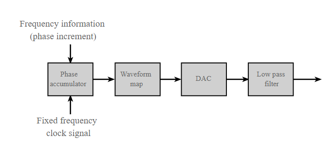
Figure 20.1 DDS block diagram
20.3.2 AD9767 Configuration Introduction
The AD9767 module uses ADI’s AD9767 DAC chip, which is a 14-bit, 125MSPS conversion rate high-performance DAC device. It supports the IQ output mode and can be used in the communications.
AD9767 interface timing requirements. As shown in Figure 20.2 below, when the rising edge of the clock comes, the data must remain stable for ts time. After the rising edge of the clock, the data must remain stable for th to be correct.
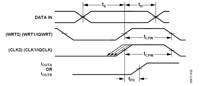
Figure 20.2 9767 interface timing diagram
20.3.3 Waveform Memory File Configuration
The waveform storage area file is dds_4096x10b_wave_init.coe. For the specific making process, refer to the use of the *.coe file in the experiment 9. The file containing the waveform information is stored in the ROM. After the project file is programmed into the FPGA, the FPGA directly reads the waveform information from the ROM and sends it to the AD9767 interface, and then outputs the corresponding waveform on the AD9767 module. The waveform storage is as shown in Figure 20.3.
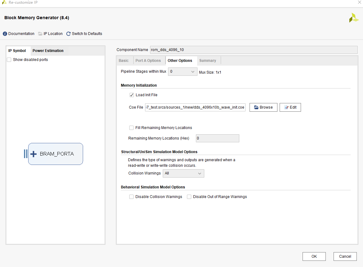
Figure 20.3 Wave file storage
20.3.4 Program Design
1. The main program includes waveform selection, mode selection, frequency adjustment, and amplitude adjustment. The specific code is as follows:
|
20.4 Experiment Varification
1. Pin assignment
| Signal Name | Port Description | Network Name | FPGA Pin |
| sys_clk_50m | System clock | C10_50MCLK | U22 |
| mode | 9767mode control | IO24 | U19 |
| wave_adjust | Waveform selection | key2 | L4 |
| a_adjust | Amplitude selection | key3 | L5 |
| f_adjust | Frequency selection | key4 | K5 |
| mode_adjust | Mode selection | key6 | P1 |
| led | Mode indicator light | LED0 | N17 |
| dac_clk | 9767 driving clock | IO28 | U14 |
| rst_n | System reset | key1 | M4 |
| data_out[0] | AD9767 data bus | IO1 | V24 |
| data_out[1] | AD9767 data bus | IO0 | U24 |
| data_out[2] | AD9767 data bus | IO5 | W23 |
| data_out[3] | AD9767 data bus | IO4 | V23 |
| data_out[4] | AD9767 data bus | IO3 | AA23 |
| data_out[5] | AD9767 data bus | IO6 | V22 |
| data_out[6] | AD9767 data bus | IO2 | AA22 |
| data_Out[7] | AD9767 data bus | IO7 | V21 |
| data_out[8] | AD9767 data bus | IO29 | V14 |
| data_out[9] | AD9767 data bus | IO30 | V16 |
| data_out[10] | AD9767 data bus | IO31 | V17 |
| data_out[11] | AD9767 data bus | IO27 | U16 |
| data_out[12] | AD9767 data bus | IO26 | U15 |
| data_out[13] | AD9767 data bus | IO25 | T15 |
2. Board verification
After the FPGA development board is programmed, press the right key (mode), and the mode indicator led0 lights up.
Then waveform can be chosen according to UP key (waveform selection), RETURN key (amplitude selection), LEFT key (frequency selection). (This experiment is only to introduce the theoretical knowledge of DDS and verify its correctness. Therefore, only four types of waveforms are set, which are sine wave, square wave, triangle wave, and sawtooth wave. The frequency and amplitude are also randomly set.) Figure 20.4 below shows four waveforms of the oscilloscope measuring the output of the 9767 module.
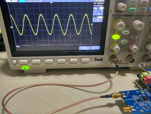
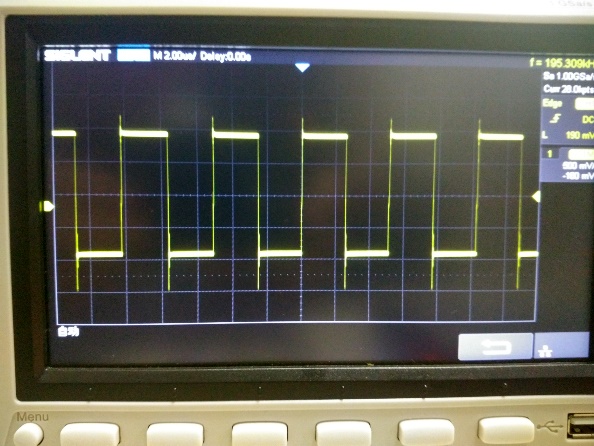
Figure 20-4a Sine wave Figure 20-4b Square wave
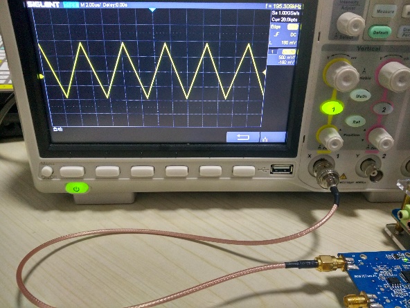
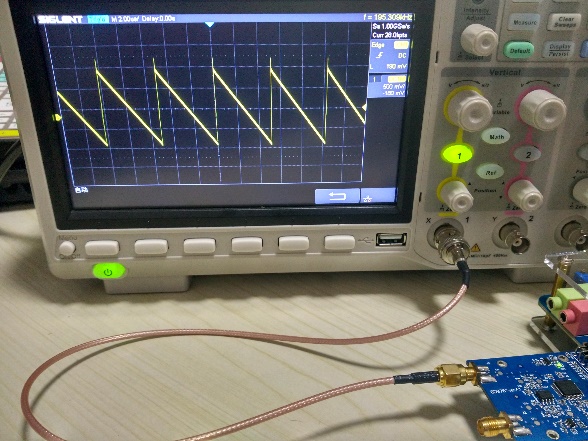
Figure 20-4c Triangle wave Figure 20-4d Sawtooth wave