High-speed ADC9226 Acquisition Experiment – Xilinx Risc-V Board FII-PRX100 Experiment 19
Experiment 19 High-speed ADC9226 Acquisition Experiment
19.1 Experiment Objective
Learn about parallel ADC collectors and master the use of ADC9226.
19.2 Experiment Implement
1. Insert the ADC9226 module face up into the FPGA development board to the GPIO2 and GPIO1 ports which are next to the red-green audio module. Write programs to use this module to test
19.3 Experiment
19.3.1 ADC9226 Module Introduction
ADC9226 module adopts AD9226 chip design of ADI Company. This chip is a monolithic, 12-bit, 65 MSPS analog-to-digital converter (ADC). It uses a single power supply and has an on-chip high-performance sample-and-hold amplifier and voltage reference. It uses a multistage differential pipelined architecture with a data rate of 65 MSPS and guarantees no missing codes over the full operating temperature range.
See Figure 19.1 for ADC9226 timing diagram.
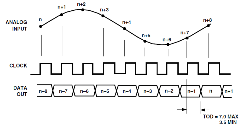
Figure19.1 ADC9226 timing diagram
From this timing diagram, we know that there is no need to configure the AD9226 chip, as long as the appropriate CLOCK is provided, the chip can perform data acquisition.
19.3.2 Program Design
-
- AD acquisition sub-module
As can be seen from Figure 19.1, the high bit of AD9226 is bit[0] and the low bit is bit [11], so the data bit order needs to be reversed in the program.
|
2.Data conversion program
The AD9226 module design uses an internal reference source. VREF is the output port of the reference source, which can be used for 1V and 2V reference voltages. It can be selected through SENCE. When SENCE is grounded, a 2V reference is provided, and when SENCE is connected to VREF, a 1V reference is provided. The module uses a 2V reference power supply. VINA input range is 1.0 ~ 3.0V.
The 22 pin of AD9226 has the function of collecting data selection. There are two input and output data formats of AD9226. For the specific format, refer to the 9226 datasheet. The 22 pin of the AD9226 module in this experiment is connected to high level, so it uses Binary Output Mode. The BCD conversion submodule has been introduced in Experiment 8 and is not repeated here.
| module volt_cal(
input wire ad_clk, input wire [11:0] ad_ch1, output [19:0] ch1_dec, output reg ch1_sig ); reg [31:0] ch1_data_reg; reg [11:0] ch1_reg; reg [31:0] ch1_vol; always @(posedge ad_clk) begin if(ad_ch1[11]==1’b1) begin ch1_reg<={1’b0,ad_ch1[10:0]}; ch1_sig <= 0; end else begin ch1_reg<={12’h800-ad_ch1[10:0]}; ch1_sig<=1; end end always @(posedge ad_clk) begin ch1_data_reg<=ch1_reg * 2000; ch1_vol<=ch1_data_reg >>11; end bcd bcd1_ist( .hex (ch1_vol[15:0]), .dec (ch1_dec), .clk (ad_clk) ); endmodule |
- 9226 module AD acquisition range selection
The attenuation range of the AD acquisition module is divided into gears. Press the UP key on the development board to switch the range.
Table 19.1 Gear shift indication table
| Gear comparison table (input voltage percentage) | Corresponding indicator |
| 4% | led0 lit |
| 8% | led0, led1 lit |
| 20% | led0, led1, led2 lit |
| 40% | led0, led1, led2, led2 lit |
|
- Main program design
The main program is divided into three sub-programs, which are AD_9226 acquisition module, data conversion calculation module volt_cal, and voltage value segment display module. The segment display part has been introduced in the previous experiment and will not be introduced here.
|
|
19.4 Experiment Verification
- Pin assignment
| Signal Name | Port Description | Network Name | FPGA Pin |
| sys_clk | System clock | C10_50MCLK | U22 |
| sys_rst_n | System reset | KEY1 | M4 |
| lg_en | ADG612 input | IO25 | T15 |
| hg_en | ADG612 input | IO24 | U19 |
| ad1_clk | Ad acquisition clock | IO28 | V14 |
| otr | Input voltage overrange flag | IO1 | V24 |
| sm_db[0] | Segment selection | SEG_PA | K26 |
| sm_db[1] | Segment selection | SEG_PB | M20 |
| sm_db[2] | Segment selection | SEG_PC | L20 |
| sm_db[3] | Segment selection | SEG_PD | N21 |
| sm_db[4] | Segment selection | SEG_PE | N22 |
| sm_db[5] | Segment selection | SEG_PF | P21 |
| sm_db[6] | Segment selection | SEG_PG | P23 |
| sm_db[7] | Segment selection | SEG_DP | P24 |
| sel[0] | Bit selection | SEG_3V3_D0 | R16 |
| sel[1] | Bit selection | SEG_3V3_D1 | R17 |
| sel[2] | Bit selection | SEG_3V3_D2 | N18 |
| sel[3] | Bit selection | SEG_3V3_D3 | K25 |
| sel[4] | Bit selection | SEG_3V3_D4 | R25 |
| sel[5] | Bit selection | SEG_3V3_D5 | T24 |
| ad1_in[0] | AD9226 acquisition data bus | IO0 | U24 |
| ad1_in[1] | AD9226 acquisition data bus | IO5 | W23 |
| ad1_in[2] | AD9226 acquisition data bus | IO4 | V23 |
| ad1_in[3] | AD9226 acquisition data bus | IO3 | AA23 |
| ad1_in[4] | AD9226 acquisition data bus | IO6 | V22 |
| ad1_in[5] | AD9226 acquisition data bus | IO2 | AA22 |
| ad1_in[6] | AD9226 acquisition data bus | IO7 | V21 |
| ad1_in[7] | AD9226 acquisition data bus | IO29 | U14 |
| ad1_in[8] | AD9226 acquisition data bus | IO30 | V16 |
| ad1_in[9] | AD9226 acquisition data bus | IO31 | V17 |
| ad1_in[10] | AD9226 acquisition data bus | IO27 | U16 |
| ad1_in[11] | AD9226 acquisition data bus | IO26 | U15 |
- Board verification
Use 1M sine wave as the signal source, AD9226 module to connect to GPIO1 and GPIO2 of 100T. Use the logic analyzer to capture the signal as shown in Figure 19.2.From the left to the right of the segment display, the first segment display is selected and lit to indicate that the input measurement voltage exceeds the AD9226 measurement range (the absolute value of VINA-VINB is less than or equal to the reference voltage, and the reference voltage of this module is 2V). The second segment display shows the sign of the input voltage (VINA-VINB). The last four digits are the input voltage value. When the input signal value is a slowly changing signal, the segment display can display the signal voltage amplitude.
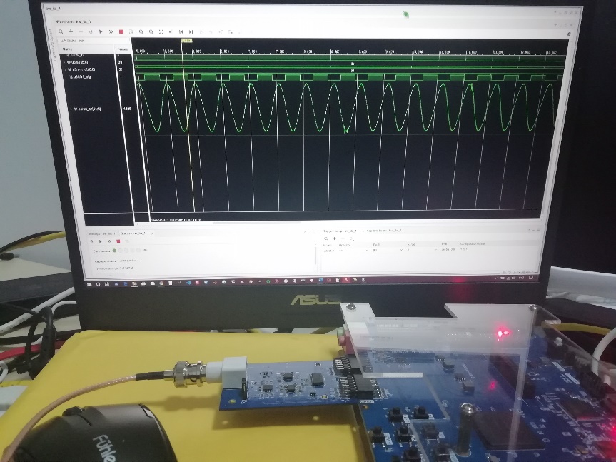
Figure 19.2 Signal waveform of AD9226 captured by logic analyzer