Photo Display Experiment of OV5640 Camera , Understand the power-on sequence of the OV5640 camera and the corresponding register configuration process – Xilinx Risc-V Board FII-PRX100 Experiment 18
Experiment 18 Photo Display Experiment of OV5640 Camera
18.1 Experiment Objective
- Understand the power-on sequence of the OV5640 camera and the corresponding register configuration process when outputting images of different resolutions
- Review previous knowledge of IIC bus
- Review previous knowledge of HDMI
18.2 Experiment Implement
- Read the power-on sequence of the OV5640 datasheet, and correctly write the power-on control program according to the peripheral module schematics.
- Correctly write the configuration program of the OV5640 camera with a resolution of 640X480 according to the timing requirements of the SCCB interface
- Based on previous experiments, write a program to store the image data collected by 5640 in the development board SRAM.
- Write a program to display the image stored in the SRAM to the monitor via HDMI.
- The refresh of the image is controlled by the keys, and the screen display image is updated every time pressing it, similar to a camera.
18.3 Experiment
Some main procedures are given below. Refer the project file for the complete program
- Ov5640 power-on initialization program design is based on the power-on timing diagram of 5640 when connected to DVDD. Shown in Figure 18.1.
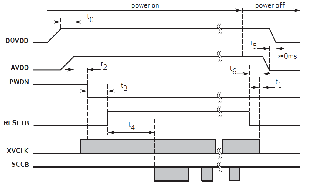
Figure 18.1 5640 power-on sequence
Power-on sequence program is as follows:
| module power_on_delay(clk_50M,reset_n_r,camera_pwup,initial_en,cam_resetb);
input clk_50M; input reset_n_r; output camera_pwup; output initial_en; (*mark_debug=”true”*)output reg cam_resetb =0; (*mark_debug=”true”*)reg [31:0]cnt1=0; reg initial_en=0; reg camera_pwup_reg=0; reg reset_n =0; assign camera_pwup=camera_pwup_reg; always @ (posedge clk_50M) reset_n<=reset_n_r ; //5ms, delay from sensor power up stable to Pwdn pull down always@(posedge clk_50M) begin if(reset_n==1’b0) cnt1<=0; else begin if (cnt1<50000000) cnt1<=cnt1+1 ; else cnt1<=cnt1 ; end end always@(posedge clk_50M) begin if(reset_n==1’b0) begin camera_pwup_reg<=0; end else begin if (cnt1==15000000) camera_pwup_reg<=1; else camera_pwup_reg<=camera_pwup_reg; end end always@(posedge clk_50M) begin if(reset_n==1’b0) begin cam_resetb <=0; end else begin if (cnt1==35000000) cam_resetb <=1; else cam_resetb <=cam_resetb ; end end always@(posedge clk_50M) begin if(reset_n==1’b0) begin initial_en<=0; end else begin if (cnt1==48000000) initial_en<=1; else initial_en<=initial_en; end end endmodule |
- 5640 chip configuration program
After the development board is powered on correctly, the OV5640 related registers will be configured. The configuration of the OV5640 chip’s internal registers is performed through the SCCB (Serial Camera Control Bus) protocol. This protocol is equivalent to a simple I2C bus. The SCCB timing is shown in Figure 18.2. When configuring, use the I2C code from previous experiment directly.
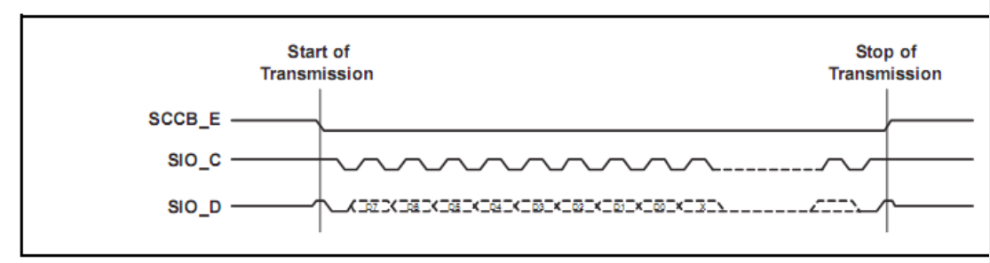
18.2 SCCB write register timing diagram
The registers required to complete the 5640 camera function are as follows:
| always@(reg_index)
begin case(reg_index) 0:reg_data<=24’h310311; 1:reg_data<=24’h300882; 2:reg_data<=24’h300842; 3:reg_data<=24’h310303; 4:reg_data<=24’h3017ff; 5:reg_data<=24’h3018ff; 6:reg_data<=24’h30341A; 7:reg_data<=24’h303713; 8:reg_data<=24’h310801; 9:reg_data<=24’h363036; 10:reg_data<=24’h36310e; 11:reg_data<=24’h3632e2; 12:reg_data<=24’h363312; 13:reg_data<=24’h3621e0; 14:reg_data<=24’h3704a0; 15:reg_data<=24’h37035a; 16:reg_data<=24’h371578; 17:reg_data<=24’h371701; 18:reg_data<=24’h370b60; 19:reg_data<=24’h37051a; 20:reg_data<=24’h390502; 21:reg_data<=24’h390610; 22:reg_data<=24’h39010a; 23:reg_data<=24’h373112; 24:reg_data<=24’h360008; 25:reg_data<=24’h360133; 26:reg_data<=24’h302d60; 27:reg_data<=24’h362052; 28:reg_data<=24’h371b20; 29:reg_data<=24’h471c50; 30:reg_data<=24’h3a1343; 31:reg_data<=24’h3a1800; 32:reg_data<=24’h3a19f8; 33:reg_data<=24’h363513; 34:reg_data<=24’h363603; 35:reg_data<=24’h363440; 36:reg_data<=24’h362201; 37:reg_data<=24’h3c0134; 38:reg_data<=24’h3c0428; 39:reg_data<=24’h3c0598; 40:reg_data<=24’h3c0600; 41:reg_data<=24’h3c0708; 42:reg_data<=24’h3c0800; 43:reg_data<=24’h3c091c; 44:reg_data<=24’h3c0a9c; 45:reg_data<=24’h3c0b40; 46:reg_data<=24’h381000; 47:reg_data<=24’h381110; 48:reg_data<=24’h381200; 49:reg_data<=24’h370864; 50:reg_data<=24’h400102; 51:reg_data<=24’h40051a; 52:reg_data<=24’h300000; 53:reg_data<=24’h3004ff; 54:reg_data<=24’h300e58; 55:reg_data<=24’h302e00; 56:reg_data<=24’h430061; 57:reg_data<=24’h501f01; 58:reg_data<=24’h440e00; 59:reg_data<=24’h5000a7; 60:reg_data<=24’h3a0f30; 61:reg_data<=24’h3a1028; 62:reg_data<=24’h3a1b30; 63:reg_data<=24’h3a1e26; 64:reg_data<=24’h3a1160; 65:reg_data<=24’h3a1f14; 66:reg_data<=24’h580023; 67:reg_data<=24’h580114; 68:reg_data<=24’h58020f; 69:reg_data<=24’h58030f; 70:reg_data<=24’h580412; 71:reg_data<=24’h580526; 72:reg_data<=24’h58060c; 73:reg_data<=24’h580708; 74:reg_data<=24’h580805; 75:reg_data<=24’h580905; 76:reg_data<=24’h580a08; 77:reg_data<=24’h580b0d; 78:reg_data<=24’h580c08; 79:reg_data<=24’h580d03; 80:reg_data<=24’h580e00; 81:reg_data<=24’h580f00; 82:reg_data<=24’h581003; 83:reg_data<=24’h581109; 84:reg_data<=24’h581207; 85:reg_data<=24’h581303; 86:reg_data<=24’h581400; 87:reg_data<=24’h581501; 88:reg_data<=24’h581603; 89:reg_data<=24’h581708; 90:reg_data<=24’h58180d; 91:reg_data<=24’h581908; 92:reg_data<=24’h581a05; 93:reg_data<=24’h581b06; 94:reg_data<=24’h581c08; 95:reg_data<=24’h581d0e; 96:reg_data<=24’h581e29; 97:reg_data<=24’h581f17; 98:reg_data<=24’h582011; 99:reg_data<=24’h582111; 100:reg_data<=24’h582215; 101:reg_data<=24’h582328; 102:reg_data<=24’h582446; 103:reg_data<=24’h582526; 104:reg_data<=24’h582608; 105:reg_data<=24’h582726; 106:reg_data<=24’h582864; 107:reg_data<=24’h582926; 108:reg_data<=24’h582a24; 109:reg_data<=24’h582b22; 110:reg_data<=24’h582c24; 111:reg_data<=24’h582d24; 112:reg_data<=24’h582e06; 113:reg_data<=24’h582f22; 114:reg_data<=24’h583040; 115:reg_data<=24’h583142; 116:reg_data<=24’h583224; 117:reg_data<=24’h583326; 118:reg_data<=24’h583424; 119:reg_data<=24’h583522; 120:reg_data<=24’h583622; 121:reg_data<=24’h583726; 122:reg_data<=24’h583844; 123:reg_data<=24’h583924; 124:reg_data<=24’h583a26; 125:reg_data<=24’h583b28; 126:reg_data<=24’h583c42; 127:reg_data<=24’h583dce; 128:reg_data<=24’h5180ff; 129:reg_data<=24’h5181f2; 130:reg_data<=24’h518200; 131:reg_data<=24’h518314; 132:reg_data<=24’h518425; 133:reg_data<=24’h518524; 134:reg_data<=24’h518609; 135:reg_data<=24’h518709; 136:reg_data<=24’h518809; 137:reg_data<=24’h518975; 138:reg_data<=24’h518a54; 139:reg_data<=24’h518be0; 140:reg_data<=24’h518cb2; 141:reg_data<=24’h518d42; 142:reg_data<=24’h518e3d; 143:reg_data<=24’h518f56; 144:reg_data<=24’h519046; 145:reg_data<=24’h5191f8; 146:reg_data<=24’h519204; 147:reg_data<=24’h519370; 148:reg_data<=24’h5194f0; 149:reg_data<=24’h5195f0; 150:reg_data<=24’h519603; 151:reg_data<=24’h519701; 152:reg_data<=24’h519804; 153:reg_data<=24’h519912; 154:reg_data<=24’h519a04; 155:reg_data<=24’h519b00; 156:reg_data<=24’h519c06; 157:reg_data<=24’h519d82; 158:reg_data<=24’h519e38; 159:reg_data<=24’h548001; 160:reg_data<=24’h548108; 161:reg_data<=24’h548214; 162:reg_data<=24’h548328; 163:reg_data<=24’h548451; 164:reg_data<=24’h548565; 165:reg_data<=24’h548671; 166:reg_data<=24’h54877d; 167:reg_data<=24’h548887; 168:reg_data<=24’h548991; 169:reg_data<=24’h548a9a; 170:reg_data<=24’h548baa; 171:reg_data<=24’h548cb8; 172:reg_data<=24’h548dcd; 173:reg_data<=24’h548edd; 174:reg_data<=24’h548fea; 175:reg_data<=24’h54901d; 176:reg_data<=24’h53811e; 177:reg_data<=24’h53825b; 178:reg_data<=24’h538308; 179:reg_data<=24’h53840a; 180:reg_data<=24’h53857e; 181:reg_data<=24’h538688; 182:reg_data<=24’h53877c; 183:reg_data<=24’h53886c; 184:reg_data<=24’h538910; 185:reg_data<=24’h538a01; 186:reg_data<=24’h538b98; 187:reg_data<=24’h558006; 188:reg_data<=24’h558340; 189:reg_data<=24’h558410; 190:reg_data<=24’h558910; 191:reg_data<=24’h558a00; 192:reg_data<=24’h558bf8; 193:reg_data<=24’h501d40; 194:reg_data<=24’h530008; 195:reg_data<=24’h530130; 196:reg_data<=24’h530210; 197:reg_data<=24’h530300; 198:reg_data<=24’h530408; 199:reg_data<=24’h530530; 200:reg_data<=24’h530608; 201:reg_data<=24’h530716; 202:reg_data<=24’h530908; 203:reg_data<=24’h530a30; 204:reg_data<=24’h530b04; 205:reg_data<=24’h530c06; 206:reg_data<=24’h502500; 207:reg_data<=24’h300802; //680×480 30 frame/ second, night mode 5fps, input clock =24Mhz, PCLK =56Mhz 208:reg_data<=24’h303511; 209:reg_data<=24’h303646; 210:reg_data<=24’h3c0708; 211:reg_data<=24’h382047; 212:reg_data<=24’h382101; 213:reg_data<=24’h381431; 214:reg_data<=24’h381531; 215:reg_data<=24’h380000; 216:reg_data<=24’h380100; 217:reg_data<=24’h380200; 218:reg_data<=24’h380304; 219:reg_data<=24’h38040a; 220:reg_data<=24’h38053f; 221:reg_data<=24’h380607; 222:reg_data<=24’h38079b; 223:reg_data<=24’h380802; 224:reg_data<=24’h380980; 225:reg_data<=24’h380a01; 226:reg_data<=24’h380be0; 227:reg_data<=24’h380c07; 228:reg_data<=24’h380d68; 229:reg_data<=24’h380e03; 230:reg_data<=24’h380fd8; 231:reg_data<=24’h381306; 232:reg_data<=24’h361800; 233:reg_data<=24’h361229; 234:reg_data<=24’h370952; 235:reg_data<=24’h370c03; 236:reg_data<=24’h3a0217; 237:reg_data<=24’h3a0310; 238:reg_data<=24’h3a1417; 239:reg_data<=24’h3a1510; 240:reg_data<=24’h400402; 241:reg_data<=24’h30021c; 242:reg_data<=24’h3006c3; 243:reg_data<=24’h471303; 244:reg_data<=24’h440704; 245:reg_data<=24’h460b35; 246:reg_data<=24’h460c22; 247:reg_data<=24’h483722; 248:reg_data<=24’h382402; 249:reg_data<=24’h500183; 250:reg_data<=24’h350300; 251:reg_data<=24’h301602; 252:reg_data<=24’h3b070a; 253:reg_data<=24’h3b0083 ; 254:reg_data<=24’h3b0000 ; default:reg_data<=24’h000000; endcase end |
- The control codes for the LED control and camera functions are as follows:
|
- Some key codes to implement the camera function:
| module pic(
input wire key3 , (*mark_debug=”true”*)output reg hdmi_valid , (*mark_debug=”true”*)output reg [15:0] fifo_hdmi_dout , (*mark_debug=”true”*)input wire hdmi_rd_en , input wire hdmi_end , input wire hdmi_req , (*dont_touch=”true”, mark_debug=”true”*)output wire [10:0] hdmi_fifo_rd_data_count , output sram1_cs_n , output sram1_we_n , output sram1_oe_n , output sram1_ub_n , output sram1_lb_n , output sram0_cs_n , output sram0_we_n , output sram0_oe_n , output sram0_ub_n , output sram0_lb_n , output [17:0] sram_addr , inout [31:0] sram_data , input wire clk_50m , input wire rst_n_50m , input wire hdmi_reg_done , input wire reg_conf_done , input wire pic_clk , input wire vga_clk , (*mark_debug=”true”*)input wire camera_href , (*mark_debug=”true”*)input wire camera_vsync, (*mark_debug=”true”*)input wire [7:0] camera_data , (*mark_debug=”true”*)output led ); (*mark_debug=”true”*)reg camera_on = 0 ; reg lock_r = 0 ; (*mark_debug=”true”*)reg wr_en = 0 ; reg [7:0] din = 0 ; (*mark_debug=”true”*)reg rec_sign = 0 ; (*mark_debug=”true”*)reg sign_we = 0 ; (*mark_debug=”true”*)reg write_ack = 0 ; (*mark_debug=”true”*)reg [1:0] camera_vsync_rr =2’b00; (*dont_touch=”true”,mark_debug=”true”*)reg [11:0]camera_h_count; (*dont_touch=”true”,mark_debug=”true”*)reg [10:0]camera_v_count; assign led=!{camera_h_count,camera_v_count} ; always @ (posedge pic_clk) camera_vsync_rr <= {camera_vsync_rr[0],camera_vsync }; always @ (posedge pic_clk) if (hdmi_reg_done&(camera_vsync_rr==2’b10)&rst_n_50m&rec_sign) sign_we <=1 ; else if (camera_vsync_rr==2’b01) sign_we <=0 ; else sign_we <=sign_we ; //Generate camera line count always @(posedge pic_clk) begin if (!reg_conf_done) camera_h_count<=1; else if((camera_href==1’b1) & (camera_vsync==1’b0)) camera_h_count<=camera_h_count+1’b1; else camera_h_count<=1; end //Generate camera column count always @(posedge pic_clk) begin if (!reg_conf_done) camera_v_count<=0; else if (camera_vsync==1’b0) begin if(camera_h_count==1280) camera_v_count<=camera_v_count+1’b1; else camera_v_count<=camera_v_count; end else camera_v_count<=0 ; end always @ (posedge pic_clk) if (reg_conf_done==0) begin wr_en <=0 ; din <=0 ; end else begin if(camera_href&sign_we) begin wr_en <=1 ; din <=camera_data ; end else begin wr_en <=0 ; din <=0 ; end end (*mark_debug=”true”*) wire valid ; (*mark_debug=”true”*) wire [31: 0] dout ; (*mark_debug=”true”*) reg rd_en =0 ; (*mark_debug=”true”*) wire [9 : 0] rd_data_count ; wire [11 : 0] wr_data_count ; fifo_8_to_32 fifo_8_to_32_inst ( .rst(~rst_n_50m), // input wire rst .wr_clk(pic_clk), // input wire wr_clk .rd_clk(clk_50m), // input wire rd_clk .din(din), // input wire [7 : 0] din .wr_en(wr_en), // input wire wr_en .rd_en(rd_en), // input wire rd_en .dout(dout), // output wire [31 : 0] dout .full(), // output wire full .empty( ), // output wire empty .valid(valid), // output wire valid .rd_data_count(rd_data_count), // output wire [9 : 0] rd_data_count .wr_data_count(wr_data_count), // output wire [11 : 0] wr_data_count .wr_rst_busy( ), // output wire wr_rst_busy .rd_rst_busy( ) // output wire rd_rst_busy ); (*mark_debug=”true”*)reg [31:0] din_sram_fifo = 32’d0 ; (*mark_debug=”true”*)reg sram_fifo_wen = 0 ; (*mark_debug=”true”*)wire[15:0] fifo_hdmi_dout_r ; (*mark_debug=”true”*)wire hdmi_valid_r ; (*dont_touch=”true”,mark_debug=”true”*) wire [9:0] hdmi_fifo_wr_data_count ; (*dont_touch=”true”,mark_debug=”true”*) wire full ; (*dont_touch=”true”,mark_debug=”true”*) wire empty ; always @ (posedge vga_clk) begin fifo_hdmi_dout <= fifo_hdmi_dout_r ; hdmi_valid <= hdmi_valid_r ; end fifo_32_to_16 fifo_32_to_16_inst ( .rst(~rst_n_50m), // input wire rst .wr_clk(clk_50m), // input wire wr_clk .rd_clk(vga_clk), // input wire rd_clk .din(din_sram_fifo), // input wire [31 : 0] din .wr_en(sram_fifo_wen), // input wire wr_en .rd_en(hdmi_rd_en), // input wire rd_en .dout(fifo_hdmi_dout_r), // output wire [15 : 0] dout .full(full), // output wire full .empty(empty), // output wire empty .valid(hdmi_valid_r), // output wire valid .rd_data_count(hdmi_fifo_rd_data_count), // output wire [10 : 0] rd_data_count .wr_data_count(hdmi_fifo_wr_data_count), // output wire [9 : 0] wr_data_count .wr_rst_busy( ), // output wire wr_rst_busy .rd_rst_busy( ) // output wire rd_rst_busy ); reg [25:0] on_counter =26’d0 ; always @(posedge clk_50m , negedge reg_conf_done) if (!reg_conf_done) begin on_counter<=0; camera_on<=1’b0; end else begin if (key3==1’b1) // If the button is not pressed, the register is 0 on_counter<=0; else if ((key3==1’b0)& (on_counter<=500000)) // If the button is pressed and //held for less than 10ms, count on_counter<=on_counter+1’b1; if (on_counter==500000) // Once the button is effective, change the display mode camera_on<=1’b1; else if (write_ack ) camera_on<=1’b0; else camera_on<=camera_on; end (*mark_debug=”true”*) wire [31:0] data_rd ; (*mark_debug=”true”*) wire data_valid ; (*mark_debug=”true”*) reg [4:0] sram_wr_st = 0 ; (*mark_debug=”true”*) reg w_cnt = 0 ; (*mark_debug=”true”*) reg [17:0] sram_addr_wr_rd = 18’d0 ; (*mark_debug=”true”*) reg [31:0] data_we = 32’d0 ; (*mark_debug=”true”*) reg [31:0] rd_data = 32’d0 ; (*mark_debug=”true”*) reg wr_en_req = 0 ; (*mark_debug=”true”*) reg rd_en_req = 0 ; (*mark_debug=”true”*) reg [8:0] hdmi_req_cnt = 0 ; always @ (posedge clk_50m , negedge reg_conf_done ,negedge rst_n_50m ) begin if ( ~rst_n_50m|~reg_conf_done) begin rec_sign <= 0 ; sram_addr_wr_rd <= 18’d0 ; sram_wr_st <= 0 ; data_we <= 32’d0 ; rd_data <= 32’d0 ; wr_en_req <= 0 ; rd_en_req <= 0 ; hdmi_req_cnt <= 0 ; end else begin case ( sram_wr_st) 0 : begin rec_sign <= 0 ; sram_addr_wr_rd <= 18’d0 ; data_we <= 32’d0 ; rd_data <= 32’d0 ; wr_en_req <= 0 ; rd_en_req <= 0 ; sram_wr_st <= 1 ; write_ack <= 0 ; end 1 : begin if (camera_on) begin sram_wr_st <= 2 ; rec_sign <= 1 ; write_ack <= 1 ; end else sram_wr_st <= 7 ; end 2 : begin write_ack <= 0 ; if (sign_we) begin data_we <= 0 ; sram_addr_wr_rd <= 0 ; wr_en_req <= 0 ; rec_sign <= 0 ; sram_wr_st <= 3 ; end else begin rec_sign <= 1 ; sram_wr_st <= 2 ; end end 3 : begin if ( sign_we ) begin if ( rd_data_count ) begin rd_en <= 1 ; sram_wr_st <= 4 ; end else begin rd_en <= 0 ; sram_wr_st <= 3 ; end end else begin rd_en <= 0 ; sram_wr_st <= 0 ; end end 4 :begin rd_en <= 0 ; data_we <= dout ; sram_addr_wr_rd <= sram_addr_wr_rd ; wr_en_req <= valid ; sram_wr_st <= 5 ; end 5: begin data_we <= dout ; sram_addr_wr_rd <= sram_addr_wr_rd ; wr_en_req <= valid; sram_wr_st <= 6 ; end 6 : begin data_we <= dout ; sram_addr_wr_rd <= sram_addr_wr_rd +1 ; wr_en_req <= valid; sram_wr_st <= 3 ; end 7: begin din_sram_fifo <= data_rd ; sram_fifo_wen <= data_valid ; if (hdmi_end) sram_wr_st <= 0 ; else begin if (hdmi_req) begin rd_en_req <=1 ; sram_addr_wr_rd<=sram_addr_wr_rd; sram_wr_st <= 8 ; hdmi_req_cnt <= 0 ; end else begin hdmi_req_cnt <= 0 ; sram_wr_st <= 7 ; end end end 8: begin sram_addr_wr_rd<=sram_addr_wr_rd+1; sram_wr_st <= 9 ; end 9 :begin sram_addr_wr_rd <= sram_addr_wr_rd + 1 ; sram_wr_st <= 10 ; hdmi_req_cnt <= hdmi_req_cnt+1 ; end 10 : begin hdmi_req_cnt <= hdmi_req_cnt+1 ; din_sram_fifo <= data_rd ; sram_fifo_wen <= data_valid ; sram_addr_wr_rd<= sram_addr_wr_rd+1 ; if (hdmi_req_cnt==318) begin rd_en_req <= 0 ; sram_wr_st <= 7 ; end end default : sram_wr_st <= 0 ; endcase end end sram_ctr sram_ctr_inst0 ( .clk_50 (clk_50m ) , .rst_n (rst_n_50m ) , .wr_en (wr_en_req) , .rd_en (rd_en_req) , .sram_addr_wr_rd (sram_addr_wr_rd) , .data_we (data_we ) , .data_rd (data_rd ) , .data_valid (data_valid ) , .sram_addr (sram_addr) , .sram_data (sram_data) , .sram1_ce (sram1_cs_n) , .sram1_oe (sram1_oe_n) , .sram1_we (sram1_we_n) , .sram1_lb (sram1_lb_n) , .sram1_ub (sram1_ub_n) , .sram0_ce (sram0_cs_n) , .sram0_oe (sram0_oe_n) , .sram0_we (sram0_we_n) , .sram0_lb (sram0_lb_n) , .sram0_ub (sram0_ub_n) ) ; endmodule |
(4) For the HDMI part, refer to the relevant HDMI content in previous experiments
18.4 Experiment Board Verification
- Pin assignment table
| Signal Name | Port Description | Network Name | FPGA Pin |
| Clk_50m | System 50M clock | C10_50MCLK | U22 |
| Reset_n | System reset signal | KEY1 | M4 |
| Clk_24 | Clock procided by PLL to 5640 | IO29 | V14 |
| Camera_data[0] | 5640 imgae data bus | IO31 | V17 |
| Camera_data[1] | 5640 imgae data bus | IO27 | U16 |
| Camera_data[2] | 5640 imgae data bus | IO2 | AA22 |
| Camera_data[3] | 5640 imgae data bus | IO7 | V21 |
| Camera_data[4] | 5640 imgae data bus | IO5 | W23 |
| Camera_data[5] | 5640 imgae data bus | IO0 | U24 |
| Camera_data[6] | 5640 imgae data bus | IO26 | U15 |
| Camera_data[7] | 5640 imgae data bus | IO28 | U14 |
| Camera_pclk | 5640 image clock | IO1 | V24 |
| Camera_href | 5640 input horizontal signal | IO25 | T15 |
| Camera_vsync | 5640 input vertical signal | IO24 | U19 |
| Camera_pwup | 5640 power up control pin | IO6 | V22 |
| Key1 | Camera on | KEY3 | L8 |
| Key2 | LED | KEY6 | P1 |
| vga_hs | Horizontal synchronization signal | HDMI_HSYNC | C24 |
| vga_vs | Vertical synchronization signal | HDMI_VSYNC | A25 |
| en | Data valid | HDMI_DE | A24 |
| vga_clk | Display clock | HDMI_CLK | B19 |
| key1 | Display switch | KEY2 | L4 |
| scl | adv7511 configured clock | I2C_SCL | R20 |
| sda | adv7511 configured data line | I2C_SDA | R21 |
| vag_r[7] | Red output | HDMI_D23 | F15 |
| vag_r[6] | Red output | HDMI_D22 | E16 |
| vag_r[5] | Red output | HDMI_D21 | D16 |
| vag_r[4] | Red output | HDMI_D20 | G17 |
| vag_r[3] | Red output | HDMI_D19 | E17 |
| vag_r[2] | Red output | HDMI_D18 | F17 |
| vag_r[1] | Red output | HDMI_D17 | C17 |
| vag_r[0] | Red output | HDMI_D16 | A17 |
| vag_g[7] | Green output | HDMI_D15 | B17 |
| vag_g[6] | Green output | HDMI_D14 | C18 |
| vag_g[5] | Green output | HDMI_D13 | A18 |
| vag_g[4] | Green output | HDMI_D12 | D19 |
| vag_g[3] | Green output | HDMI_D11 | D20 |
| vag_g[2] | Green output | HDMI_D10 | A19 |
| vag_g[1] | Green output | HDMI_D9 | B20 |
| vag_g[0] | Green output | HDMI_D8 | A20 |
| vag_b[7] | Blue output | HDMI_D7 | B21 |
| vag_b[6] | Blue output | HDMI_D6 | C21 |
| vag_b[5] | Blue output | HDMI_D5 | A22 |
| vag_b[4] | Blue output | HDMI_D4 | B22 |
| vag_b[3] | Blue output | HDMI_D3 | C22 |
| vag_b[2] | Blue output | HDMI_D2 | A23 |
| vag_b[1] | Blue output | HDMI_D1 | D21 |
| vag_b[0] | Blue output | HDMI_D0 | B24 |
| Uart_rx | Serial receive | TTL_TX | L17 |
| Uart_tx | Serial transmit | TTL_RX | L18 |
| Sram_data[0] | SRAM data bus | D0 | U21 |
| Sram_data[1] | SRAM data bus | D1 | U25 |
| Sram_data[2] | SRAM data bus | D2 | W26 |
| Sram_data[3] | SRAM data bus | D3 | Y26 |
| Sram_data[4] | SRAM data bus | D4 | AA25 |
| Sram_data[5] | SRAM data bus | D5 | AB26 |
| Sram_data[6] | SRAM data bus | D6 | AA24 |
| Sram_data[7] | SRAM data bus | D7 | AB24 |
| Sram_data[8] | SRAM data bus | D8 | AC24 |
| Sram_data[9] | SRAM data bus | D9 | AC26 |
| Sram_data[10] | SRAM data bus | D10 | AB25 |
| Sram_data[11] | SRAM data bus | D11 | Y23 |
| Sram_data[12] | SRAM data bus | D12 | Y25 |
| Sram_data[13] | SRAM data bus | D13 | W25 |
| Sram_data[14] | SRAM data bus | D14 | V26 |
| Sram_data[15] | SRAM data bus | D15 | U26 |
| Sram_data[16] | SRAM data bus | D16 | T14 |
| Sram_data[17] | SRAM data bus | D17 | T17 |
| Sram_data[18] | SRAM data bus | D18 | W18 |
| Sram_data[19] | SRAM data bus | D19 | U17 |
| Sram_data[20] | SRAM data bus | D20 | V18 |
| Sram_data[21] | SRAM data bus | D21 | T18 |
| Sram_data[22] | SRAM data bus | D22 | W19 |
| Sram_data[23] | SRAM data bus | D23 | T19 |
| Sram_data[24] | SRAM data bus | D24 | W21 |
| Sram_data[25] | SRAM data bus | D25 | Y22 |
| Sram_data[26] | SRAM data bus | D26 | Y21 |
| Sram_data[27] | SRAM data bus | D27 | U20 |
| Sram_data[28] | SRAM data bus | D28 | T20 |
| Sram_data[29] | SRAM data bus | D29 | W20 |
| Sram_data[30] | SRAM data bus | D30 | Y20 |
| Sram_data[31] | SRAM data bus | D31 | V19 |
| Sram_addr[0] | SRAM address bus | A0 | E26 |
| Sram_addr[1] | SRAM address bus | A 1 | E25 |
| Sram_addr[2] | SRAM address bus | A 2 | D26 |
| Sram_addr[3] | SRAM address bus | A 3 | D25 |
| Sram_addr[4] | SRAM address bus | A 4 | G22 |
| Sram_addr[5] | SRAM address bus | A 5 | H18 |
| Sram_addr[6] | SRAM address bus | A 6 | M15 |
| Sram_addr[7] | SRAM address bus | A 7 | M16 |
| Sram_addr[8] | SRAM address bus | A 8 | L15 |
| Sram_addr[9] | SRAM address bus | A 9 | K23 |
| Sram_addr[10] | SRAM address bus | A 10 | J25 |
| Sram_addr[11] | SRAM address bus | A 11 | K22 |
| Sram_addr[12] | SRAM address bus | A 12 | H26 |
| Sram_addr[13] | SRAM address bus | A 13 | J26 |
| Sram_addr[14] | SRAM address bus | A 14 | J24 |
| Sram_addr[15] | SRAM address bus | A 15 | G25 |
| Sram_addr[16] | SRAM address bus | A 16 | G24 |
| Sram_addr[17] | SRAM address bus | A 17 | J21 |
| Sram_addr[18] | SRAM address bus | A 18 (invalid pin) | J23 |
| Sram0_cs_n | 0th SRAM enable | CE_N_SRAM0 | F25 |
| Sram0_we_n | 0th SRAM write enable | OE_N_SRAM0 | L19 |
| Sram0_oe_n | 0th SRAM read enable | WE_N_SRAM0 | H23 |
| Sram0_ub_n | 0th SRAM high byte enable | UE_N_SRAM0 | H24 |
| Sram0_lb_n | 0th SRAM low byte enable | LE_N_SRAM0 | G26 |
| Sram0_cs_n | 1st SRAM enable | CE_N_SRAM1 | E23 |
| Sram0_we_n | 1st SRAM write enable | OE_N_SRAM1 | J18 |
| Sram0_oe_n | 1st SRAM read enable | WE_N_SRAM1 | F23 |
| Sram0_ub_n | 1st SRAM high byte enable | UE_N_SRAM1 | F24 |
| Sram0_lb_n | 1st SRAM low byte enable | LE_N_SRAM1 | K20 |
| Led0 | OV5640 register configuration indicator | LED0 | N17 |
| Led1 | ADV7511 register configuration indicator | LED1 | M19 |
- Board verification
After the board is programmed, led0 and led1 light up, indicating that the OV5640 and ADV7511 configurations are complete.
Push button RIGHT has the function of turning on and off the LED fill light.
Press the RETURN button once, the camera will take a picture and display it on the display screen of the HDMI interface. Actual board test results are shown in Figure 18.3.
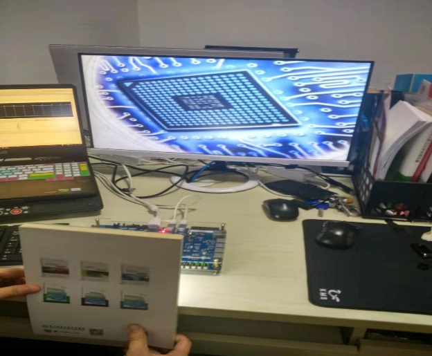
Figure 18.3a 5640 taken image Figure 18.3b 5640 display shows taken picture