Xilinx Risc-V Board Tutorial : Button Debounce Design and Experimental- FII-PRX100 FPGA Board Experiment 5
Experiment 5 Button Debounce Design and Experimental
1.Experiment Objective
-
- Review the design of blinking LED
- Learn the principle of button debounce, and adaptive programming
- Learn the connection and use of the FII-PRX100T button schematics
- Integrated application of button debounce and another compatible program design
2.Experiment
- Button debounce principle
Usually, the switches used for the buttons are mechanical elastic switches. When the mechanical contacts are opened and closed, due to the elastic action of the mechanical contacts, a push button switch does not immediately turn on when closed, nor is it off when disconnected. Instead, there is some bouncing when connecting and disconnecting. See Fig 5. 1
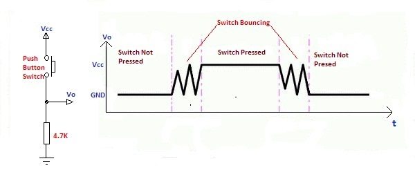
Fig 5. 1 Button bounce principle
The length of the button’s stable closing time is determined by the operator. It usually takes more than 100ms. If you press it quickly, it will reach 40-50ms. It is difficult to make it even shorter. The bouncing time is determined by the mechanical characteristics of the button. It is usually between a few milliseconds and tens of milliseconds. To ensure that the program responds to the button’s every on and off, it must be debounced. When the change of the button state is detected, it should not be immediately responding to the action, but waiting for the closure or the disconnection to be stabilized before processing. Button debounce can be divided into hardware debounce and software debounce.
In most of cases, we use software or programs to achieve debounce. The simplest debounce principle is to wait for a delay time of about 10ms after detecting the change of the button state, and then perform the button state detection again after the bounce disappears. If the state is the same as the previous state just detected, the button can be confirmed. The action has been stabilized. This type of detection is widely used in traditional software design. However, as the number of button usage increases, or the buttons of different qualities will react differently. If the delay is too short, the bounce cannot be filtered out. When the delay is too long, it affects the sensitivity of the button.
This chapter introduces an adaptive button debounce method: starts timing when a change in the state of the button is detected. If the state changes within 10ms, the button bouncing exists. It returns to the initial state, clears the delay counter, and re-detects the button state until the delay counter counts to 10ms. The same debounce method is used for pressing and releasing the button. The flow chart is shown in Fig 5. 2.
- Code for button debouncing
Verilog code is as follows:
| module pb_ve(
input sys_clk, //100 MHz input sys_rst,//System reset input ms_f, //millisecond pulse input keyin, //input state of the key output keyout //Output status of the key. Every time releasing the button, only one system ); //clock pulase outputs
reg keyin_r; //Input latch to eliminate metastable reg keyout_r;//Output pulse //push_button vibrating elemination reg [1:0] ve_key_st; //State machine status bit reg [3:0] ve_key_count;//delay counter
always@(posedge sys_clk) keyin_r<=keyin; // Input latch to eliminate metastable
always@(posedge sys_clk) if(sys_rst) begin keyout_r <=1’b0; ve_key_count <=0; ve_key_st <=0; end else case(ve_key_st) 0:begin keyout_r<=1’b0; ve_key_count <=0; if(!keyin_r) ve_key_st <=1; end 1:begin if(keyin_r) ve_key_st <=0; else begin if(ve_key_count==10) begin ve_key_st <=2; end else if(ms_f) ve_key_count<=ve_key_count+1; end end 2:begin ve_key_count <=0; if(keyin_r) ve_key_st <=3; end 3:begin if(!keyin_r) ve_key_st <=2; else begin if(ve_key_count==10) begin ve_key_st <=0; keyout_r<=1’b1;//After releasing debounce, output a synchronized end //clock pulse else if(ms_f) ve_key_count<=ve_key_count+1;
end end default:; endcase assign keyout=keyout_r; endmodule |
Case 0 and 1 debounce the button press state. Case 2 and 3 debounce the button release state. After finishing the whole debounce procedure, the program outputs a synchronized clock pulse.
- Button debounce flow chart
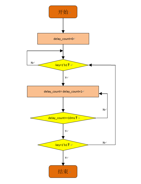
End
Start
Fig 5. 2 Button debounce flow chart
- Combine running LED design and modify the button debounce.
- Build new project
- Create a PLL symbol
- Create a button debounce symbol (See the Verilog HDL code in this experiment)
- Create a top-level file key_filter
| module key_filter(
input clk_in, input left, input right, input wire rst, output wire [7:0] led
); wire sys_rst_s= sys_rst; reg sys_rst; wire ms_f; wire s_f ; wire sys_clk; wire locked; wire left_flag, right_flag ; reg left_cmd=0; reg right_cmd =0; block_counter block_counter_inst(
. sys_rst ( sys_rst_s), . sys_clk (sys_clk), . ms_f(ms_f), . s_f (s_f) ); LED_shifting LED_shifting_inst ( . rst(sys_rst_s) , . sys_clk(sys_clk), .key_left(left_cmd), .key_right(right_cmd), .s_f(s_f), . led(led) ); pb_ve pb_ve_inst1( .sys_clk (sys_clk), .sys_rst (sys_rst_s), .ms_f (ms_f ), .keyin (left ), .keyout (left_flag ) ); pb_ve pb_ve_inst2( .sys_clk (sys_clk), .sys_rst (sys_rst_s), .ms_f (ms_f ), .keyin (right ), .keyout (right_flag ) ); always @ ( posedge sys_clk ) if (sys_rst_s) {right_cmd,left_cmd}<=2’b00; else begin case({right_flag,left_flag}) 0: {right_cmd,left_cmd}<={right_cmd,left_cmd}; 1: {right_cmd,left_cmd}<=2’b01; 2: {right_cmd,left_cmd}<=2’b10; 3: {right_cmd,left_cmd}<={right_cmd,left_cmd}; endcase end always @ (posedge sys_clk ) sys_rst<=!locked; pll pll_inst( .clk_out1(sys_clk), .reset(!rst), .locked(locked), .clk_in1(clk_in) );
endmodule |
3.Hardware Design
- Button schematics
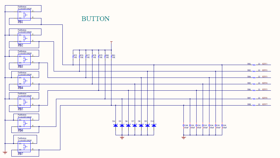
Fig 5. 4 Button schematics
- FPGA pin mapping
| Signal Name | Port Description | Network Label | FPGA Pin |
| inclk_in | System clock 50 MHz | C10_50MCLK | U22 |
| rst | Reset, high by default | KEY1 | M4 |
| led0 | LED 0 | LED0 | N17 |
| led1 | LED 1 | LED1 | M19 |
| led2 | LED 2 | LED2 | P16 |
| led3 | LED 3 | LED3 | N16 |
| led4 | LED 4 | LED4 | N19 |
| led5 | LED 5 | LED5 | P19 |
| led6 | LED 6 | LED6 | N24 |
| led7 | LED 7 | LED7 | N23 |
| left | Press left | KEY4 | K5 |
| right | Press right | KEY6 | P1 |
-
- Compile and debug
- Download the program to the board and observe the test result. See Fig 5. 5
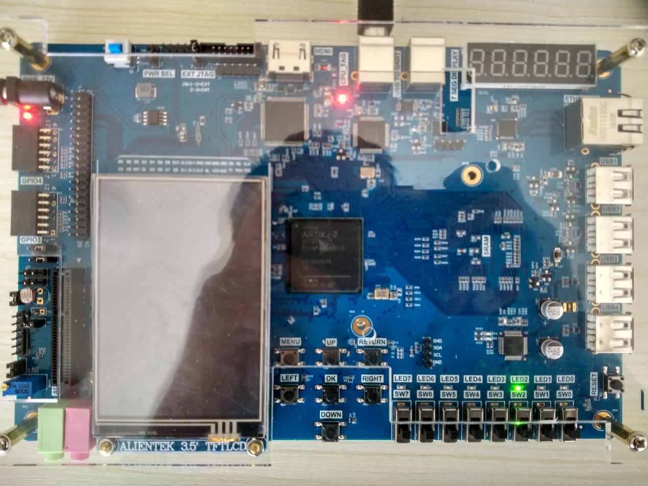
Fig 5. 5 Test Result
- Observe the test results. By default, 8 LEDs are off. Press the left button to switch the flow mode on the left side of the LED. Press the right button on the right side of the LED to switch between the flow mode. While holding down the left and right buttons, the LED remains in its original state.