Xilinx Risc-V Board Tutorial : Digital Clock Comprehensive Design Experiment- FII-PRX100 FPGA Board Experiment 6
Experiment 6 Digital Clock Comprehensive Design Experiment
1.Experiment Objective
-
- Design month, day, hour, minute, and second digital clock experiments, using 6 segment decoders
-
-
- 60 seconds carried to the minute
- 60 minutes carried to the hour
- 24 hours carried to the day
- 30 days carried to the month, and reset all
-
-
- Set four keys: menu, left, up, down
- The menu key controls the calibration function to switch between clock, date, and alarm.
- The left key selects which value is currently calibrated
- The Up and down keys add 1 and subtract 1 calibration to the data to be calibrated requires that the corresponding segment decoder is flashed.
- Modulate the design so that it can be reused
- Learn to use the module parameters
- Learn to use the timing analysis function of Vivado and correctly constrain the clock signal
- Design month, day, hour, minute, and second digital clock experiments, using 6 segment decoders
2.Design Procedure
- Build new project
-
- Project name is calendar_counter
- Select the device 10CL040YF484CG
- The top-level entity is calendar_counter.bdf or calendar_counter.v (Here the Verilog file is used)
-
- Design and integrate of submodule
-
- PLL module
- Frequency divider
- Button debounce module
- Counting module dual_num_count.v
-
Design a universal 2-bit counter that uses the parameter to specify the specified count setting.
| Module dual_num_count
#(parameter PAR_COUNTA=9, parameter PAR_COUNTB=5 ) ( input i_sys_clk, input i_ext_rst, input i_adj_up, input i_adj_down, input [1:0] i_adj_sel, input i_trig_f, output reg o_trig_f, output reg [3:0] o_counta, output reg [3:0] o_countb ); always@(posedge i_sys_clk) if(!i_ext_rst)begin o_counta <=0; o_countb <=0; o_trig_f <=1’b0; end else begin o_trig_f<=1’b0; if(i_adj_up)begin if(!i_adj_sel[0])begin if(o_counta==9) o_counta<=0; else o_counta<=o_counta+1; end else if(!i_adj_sel[1]) begin if(o_countb==9) o_countb<=0; else o_countb<=o_countb+1; end end else if(i_adj_down) begin if(!i_adj_sel[0])begin if(o_counta==0) o_counta<=9; else o_counta<=o_counta-1; end else if(!i_adj_sel[1])begin if(o_countb==0) o_countb<=9; else o_countb<=o_countb-1; end end else if(i_trig_f) begin if((o_countb==PAR_COUNTB)&&(o_counta==PAR_COUNTA)) begin o_counta<=4’d0; o_countb<=0; o_trig_f<=1’b1; end else begin if(o_counta==9)begin o_counta<=4’d0; o_countb<=o_countb+1; end else begin o_counta<=o_counta+1; end end end end endmodule |
- Button debounce
| module pb_ve(
input sys_clk, input sys_rst, input ms_f, input keyin, output keyout ); reg keyin_r; reg keyout_r; //push_button vibrating elemination reg [1:0] ve_key_st; reg [3:0] ve_key_count; always@(posedge sys_clk) keyin_r<=keyin; always@(posedge sys_clk) if(sys_rst) begin keyout_r <=1’b0; ve_key_count <=0; ve_key_st <=0; end else case(ve_key_st) 0:begin keyout_r<=1’b0; ve_key_count <=0; if(!keyin_r) ve_key_st <=1; end 1:begin if(keyin_r) ve_key_st <=0; else begin if(ve_key_count==10) begin ve_key_st <=2; end else if(ms_f) ve_key_count<=ve_key_count+1;
end end 2:begin ve_key_count <=0; if(keyin_r) ve_key_st <=3; end 3:begin if(!keyin_r) ve_key_st <=2; else begin if(ve_key_count==10) begin ve_key_st <=0; keyout_r<=1’b1; end else if(ms_f) ve_key_count<=ve_key_count+1; end end default:; endcase assign keyout=keyout_r; endmodule |
- Top-level entity design
|
module calendar_counter(
input rst, input left, //key4 input right, input up, input down, input inclk, //c0_50Mclk output reg [6:0] seven_sega, outpu reg disp_pa, output reg [5:0] scan );
wire sys_clk; wire pll_locked; reg sys_rst; reg ext_rst;
reg [7:0] us_reg; reg [9:0] ms_reg; reg [9:0] s_reg; reg us_f,ms_f,s_f; wire min_f,hr_f,day_f;
reg [3:0] counta;
wire [3:0] count_secl,count_sech; wire [3:0] count_minl,count_minh; wire [3:0] count_hrl,count_hrh;
wire [3:0] count_dayl,count_dayh;
reg [6:0]seven_seg_ra; reg [7:0]disp_p_r;
wire left_r,right_r; wire up_r,down_r;
always@(posedge sys_clk) begin sys_rst<=!pll_locked; ext_rst<=rst; end
always@(posedge sys_clk) if(sys_rst) begin us_reg<=0; us_f<=1’b0; end else begin us_f<=1’b0; if(us_reg==99)begin us_reg<=0; us_f<=1’b1; end else begin us_reg<=us_reg+1; end
end
always@(posedge sys_clk) if(sys_rst) begin ms_reg<=0; ms_f<=1’b0; end else begin ms_f<=1’b0; if(us_f) begin if(ms_reg==999)begin ms_reg<=0; ms_f<=1’b1; end else ms_reg<=ms_reg+1; end end
always@(posedge sys_clk) if(sys_rst) begin s_reg<=0; s_f<=1’b0; end else begin s_f<=1’b0; if(ms_f)begin if(s_reg==999)begin s_reg<=0; s_f<=1’b1; end else s_reg<=s_reg+1; end end dual_num_count #(.PAR_COUNTA(9), .PAR_COUNTB(5) ) dual_num_count_sec ( .i_sys_clk (sys_clk), .i_ext_rst (ext_rst), .i_adj_up (up_r), .i_adj_down (down_r), .i_adj_sel (disp_p_r[1:0]), .i_trig_f (s_f), .o_trig_f (min_f), .o_counta (count_secl), .o_count (count_sech) );
dual_num_count #(.PAR_COUNTA(9), .PAR_COUNTB(5) ) dual_num_count_min ( .i_sys_clk(sys_clk), .i_ext_rst (ext_rst), .i_adj_up (up_r), .i_adj_down (down_r), .i_adj_sel (disp_p_r[3:2]), .i_trig_f (min_f), .o_trig_f (hr_f), .o_counta (count_minl), .o_countb (count_minh) );
dual_num_count #(.PAR_COUNTA(3),.PAR_COUNTB(2)) dual_num_count_hr ( .i_sys_clk (sys_clk), .i_ext_rst (ext_rst), .i_adj_up (up_r), .i_adj_down (down_r), .i_adj_sel (disp_p_r[5:4]), .i_trig_f (hr_f), .o_trig_f (day_f), .o_counta (count_hrl), .o_countb (count_hrh) );
dual_num_count #(.PAR_COUNTA(0), .PAR_COUNTB(3) ) dual_num_count_day ( .i_sys_clk (sys_clk), .i_ext_rst (ext_rst), .i_adj_up (up_r), .i_adj_down (down_r), .i_adj_sel (disp_p_r[7:6]), .i_trig_f (day_f), .o_trig_f (), .o_counta (count_dayl), .o_countb (count_dayh) );
always@(posedge sys_clk) if(!ext_rst) begin disp_p_r<=8’b1111_1110; end else begin if(left_r) disp_p_r<={disp_p_r[6:0],disp_p_r[7]}; else if(right_r) disp_p_r<={disp_p_r[0],disp_p_r[7:1]}; end reg [2:0] scan_st;
always@(posedge sys_clk) if(!ext_rst) begin scan<=6’b11_1111; counta<=4’b0; disp_pa<=1’b1; scan_st<=0; end else case(scan_st) 0:begin scan <=6’b11_1110; counta <=count_secl; disp_pa<=disp_p_r[0]; if(ms_f) scan_st<=1; end 1:begin scan<=6’b11_1101; counta<=count_sech; disp_pa<=disp_p_r[1]; if(ms_f) scan_st<=2; end 2:begin scan<=6’b11_1011; counta<=count_minl; disp_pa<=disp_p_r[2]; if(ms_f) scan_st<=3; end 3:begin scan<=6’b11_0111; counta<=count_minh; disp_pa<=disp_p_r[3]; if(ms_f) scan_st<=4; end 4:begin scan<=6’b10_1111; counta<=count_hrl; disp_pa<=disp_p_r[4]; if(ms_f) scan_st<=5; end 5:begin scan<=6’b01_1111; counta<=count_hrh; disp_pa<=disp_p_r[5]; if(ms_f) scan_st<=0; end default:scan_st<=0; endcase
always@(*) case(counta) 0:seven_seg_ra<=7’b100_0000; 1:seven_seg_ra<=7’b111_1001; 2:seven_seg_ra<=7’b010_0100; 3:seven_seg_ra<=7’b011_0000; 4:seven_seg_ra<=7’b001_1001; 5:seven_seg_ra<=7’b001_0010; 6:seven_seg_ra<=7’b000_0010; 7:seven_seg_ra<=7’b111_1000; 8:seven_seg_ra<=7’b000_0000; 9:seven_seg_ra<=7’b001_0000; default:seven_seg_ra<=7’b100_0000; endcase always@(posedge sys_clk) seven_sega<=seven_seg_ra; pb_ve pb_ve_left ( .sys_clk (sys_clk), .sys_rst (sys_rst), .ms_f (ms_f), .keyin (left), .keyout (left_r) );
pb_ve pb_ve_right ( .sys_clk (sys_clk), .sys_rst (sys_rst), .ms_f (ms_f), .keyin (right), .keyout (right_r) ); pb_ve pb_ve_up ( .sys_clk (sys_clk), .sys_rst (sys_rst), .ms_f (ms_f), .keyin (up), .keyout (up_r) ); pb_ve pb_ve_down ( .sys_clk (sys_clk), .sys_rst (sys_rst), .ms_f (ms_f), .keyin (down), .keyout (down_r) );
calendar_pll calendar_pll ( .reset (1’b0), .inclk (inclk), .c0 (sys_clk), .locked (pll_locked) );
endmodule |
- Lock the Pins
| Signal Name | Port Description | Network Label | FPGA Pin |
| inclk | System clock, 50 MHz | C10_50MCLK | U22 |
| rst | Reset, high by default | KEY1 | M4 |
| seven_seg[0] | Segment a | SEG_PA | K26 |
| seven_seg[1] | Segment b | SEG_PB | M20 |
| seven_seg[2] | Segment c | SEG_PC | L20 |
| seven_seg[3] | Segment d | SEG_PD | N21 |
| seven_seg[4] | Segment e | SEG_PE | N22 |
| seven_seg[5] | Segment f | SEG_PF | P21 |
| seven_seg[6] | Segment g | SEG_PG | P23 |
| seven_seg[7] | Segment h | SEG_DP | P24 |
| scan[0] | Segment 6 | SEG_3V3_D5 | T24 |
| scan[1] | Segment 5 | SEG_3V3_D4 | R25 |
| scan[2] | Segment 4 | SEG_3V3_D3 | K25 |
| scan[3] | Segment 3 | SEG_3V3_D2 | N18 |
| scan[4] | Segment 2 | SEG_3V3_D1 | R18 |
| scan[5] | Segment 1 | SEG_3V3_D0 | R6 |
| left | Left button | KEY4 | K5 |
| right | Right button | KEY6 | P1 |
| up | Up button | KEY2 | L4 |
| down | Bottom button | KEY2 | R7 |
- Compile
- Download the program to the develop board for verification
-
- Observe the test result
- Use the left, right keys to move the decimal point of the segment decoder
- Use up, down keys to calibrate time
-
The test result is shown in Fig 6. 1, displaying time 10:27:05
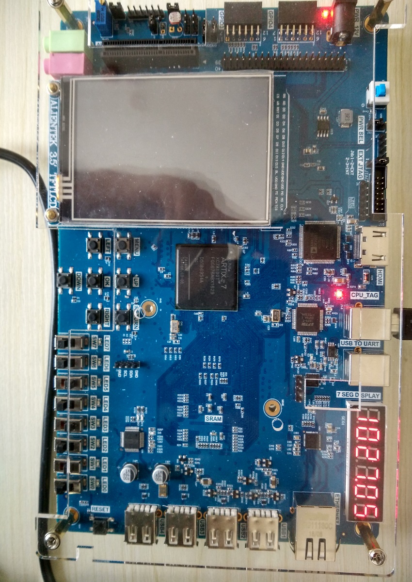
Fig 6. 1 Test result
3.Create an XDC File to Constrain the Clock
- Create constrain file
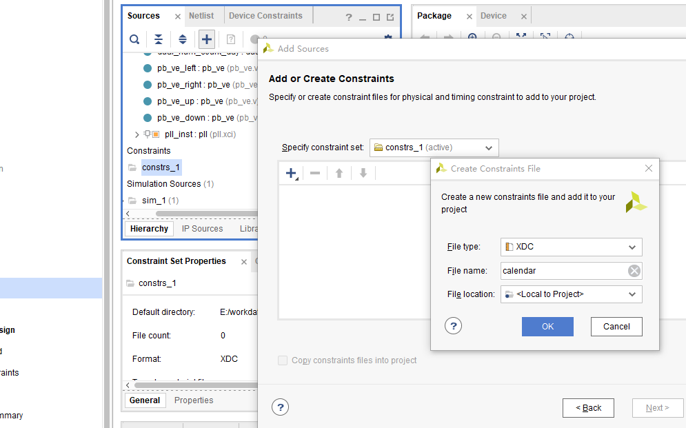
Fig 6. 2 Craete SDC file
XDC file is as follows:
# Create Clock
create_clock -period 20 -name inclk -waveform {0.000 10.000} [get_ports inclk]
- Improve the precision when using up, down to calibrate
-
- The maximum value is automatic recognized, such as in the sexagesimal decimal digit calibration time, if the value reaches 5, the next Up will make the value become 0. When the timing of Down is reduced to 0, the next Down pulse will automatically change to 5.
- Compile, and download the program to the develop board
- Program to the flash memory
-