Study the internal memory block of FPGA, Study the format of *.mif and how to edit *.mif file to configure the contents of ROM : Use of ROM – FII-PRX100 Risc-V FPGA Board Experiment 9
Experiment 9 Use of ROM
1.Experiment Objective
- Study the internal memory block of FPGA
- Study the format of *.mif and how to edit *.mif file to configure the contents of ROM
- Learn to use RAM, read and write RAM
2.Experiment Design
-
- Design 16 outputs ROM, address ranging 0-255
- Interface 8-bit switch input as ROM’s address
- Segment decoders display the contents of ROM and require conversion of hexadecimal to BCD output.
3.Design Procedure
- Create a coe file. This experiment *.coe file is generated based on Matlab2018. The *.m file is as follows:
| % –by Fraser Innovation Inc–
% function : create .coe clear all; close all; clc; depth= 256; width =16; fid_s = fopen(‘test_rom.coe’, ‘w+’); fprintf(fid_s, ‘MEMORY_INITIALIZATION_RADIX = %d;\n’,width); fprintf(fid_s, ‘%s\n’, ‘MEMORY_INITIALIZATION_VECTOR =’); for i=0:depth–1 data =i*i; b=dec2hex(data); fprintf(fid_s, ‘%s’, b); fprintf(fid_s, ‘%s\n’, ‘,’); end fclose(fid_s); disp(‘=======mif file completed========’); |
- *.coe file syntax is shown in Fig 9. 1.
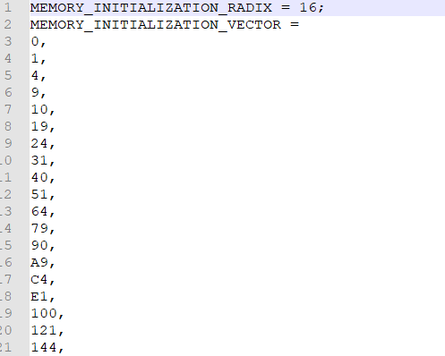
Fig 9. 1 *.coe file syntax
- Create new project, rom_test, select device XC7A100TFGG676-2
- Click IP Catalog, and input ROM in the search box. Choose Block Memory Generator. See Fig 9. 2.
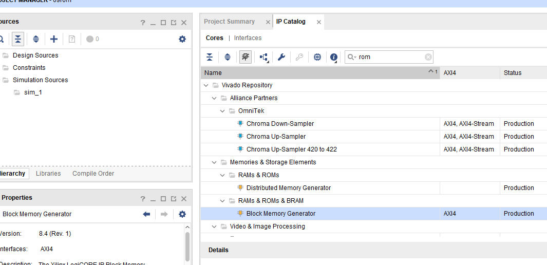
Fig 9. 2 Use of ROM IP core
- Select the memory type be Single Port ROM. See Fig 9. 3.
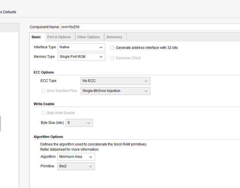
Fig 9. 3 Memory type selection
- Click Port A Options tag. Set as shown in Fig 9. 4.
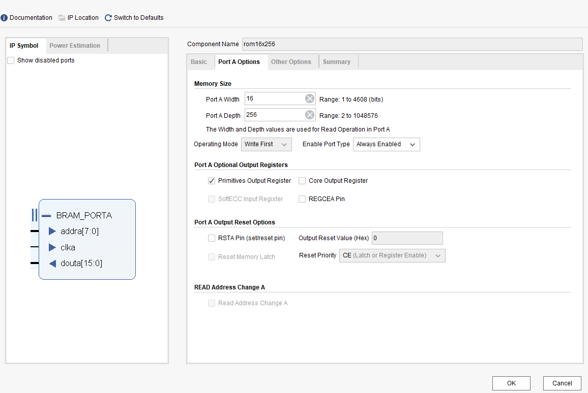
Fig 9. 4 Port memory width setting
- Click the Other Options tab shown in Fig 9. 5, select the Load Init File check box, set the correct *.coe file location, and initialize the rom.
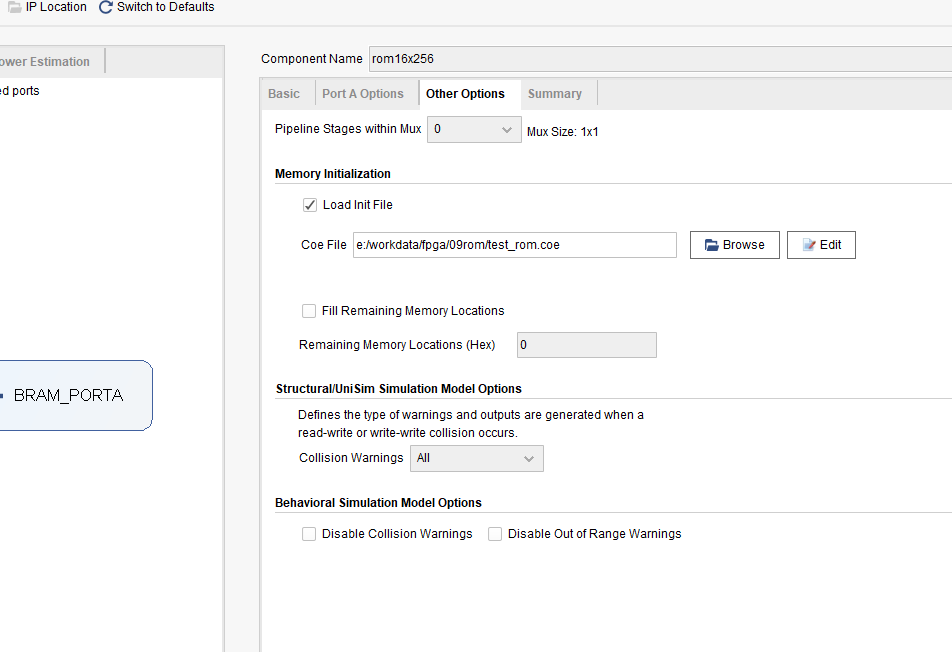
Fig 9. 5 ROM initialization
- Set others as default
- Click OK to finish setting for IP core. Generate other files related as default setting.
- Create top-level entity, rom_test.v
- Add PLL (Input clock 50 MHz, output clock 100 MHz)
- Add us_ms_s_div.v and instantiate it. Refer previous experiments for more
- Add HEX_BCD and instantiate it
- The code is given below:
| module rom_test(
input rst, input inclk, input [7:0] sw, output reg[5:0] scan, output reg[6:0] seven_sega );
wire [15:0] rom_q; wire sys_clk; wire BD_clk; wire sys_rst; wire u_f; wire m_f; wire sf; reg [7:0] count; reg [5:0] counta; reg [6:0] seven_seg_ra;
wire [3:0] ones; wire [3:0] tens; wire [3:0] hundreds; wire [3:0] thousands; wire [3:0] ten_thousands;
reg [3:0] ones_r; reg [3:0] tens_r; reg [3:0] hundreds_r; reg [3:0] thousands_r; reg [3:0] ten_thousands_r;
reg [3:0] ones_x; reg [3:0] tens_x; reg [3:0] hundreds_x; reg [3:0] thousands_x; reg [3:0] ten_thousands_x; always@(posedge BCD_clk) begin ones_x <= ones; tens_x <= tens; hundreds_x <= hundreds; thousands_x <= thousands; ten_thousands_x <= ten_thousands; end always@(posedge sys_clk) if(sys_rst) begin count <= 0; ones_r <= 0; tens_r <= 0; hundreds_r <= 0; thousands_r <= 0; ten_thousands_r <= 0; end else if(s_f) begin count <= count+1; ones_r <= ones_x; tens_r <= tens_x; hundreds_r <= hundreds_x; thousands_r <= thousands_x; ten_thousands_r <= ten_thousands_x; end
reg ext_rst; always@(posedge sys_clk) ext_rst<=rst; reg [2:0] scan_st;
always@(posedge sys_clk) if(!ext_rst) begin scan<=6’b11_1111; counta<=4’b0;
scan_st<=0; end
else case(scan_st)
0 : begin scan <= 6’b11_1110; counta <= ones_r; if( ms_f ) scan_st <= 1; end
1 : begin scan <=6’b11_1101; counta <=tens_r; if ( ms_f ) scan_st<=2; end
2 : begin scan <=6’b11_1011; counta <=hundreds_r; if(ms_f) scan_st<=3; end
3 : begin scan <=6’b11_0111; counta <=thousands_r; if(ms_f) scan_st<=4; end
4 : begin scan <=6’b10_1111; counta <=ten_thousands_r; if(ms_f) scan_st<=5; end
5 : begin scan <=6’b01_1111; counta <=0; if (ms_f) scan_st<=0; end
default:scan_st<=0; endcase always@(*) case(counta) 0 : seven_sega <= 7’b100_0000 ; 1 : seven_sega <= 7’b111_1001 ; 2 : seven_sega <= 7’b010_0100 ; 3 : seven_sega <= 7’b011_0000 ; 4 : seven_sega <= 7’b001_1001 ; 5 : seven_sega <= 7’b001_0010 ; 6 : seven_sega <= 7’b000_0010 ; 7 : seven_sega <= 7’b111_1000 ; 8 : seven_sega <= 7’b000_0000 ; 9 : seven_sega <= 7’b001_0000 ; default: seven_sega<=7’b100_0000 ; endcase
pll_sys_rst pll_sys_rst_inst( .clk_in(inclk), .sys_clk(sys_clk), .BCD_clk(BCD_clk), .sys_rst(sys_rst) );
us_ms_s_div us_ms_s_div_inst ( .sys_rst(sys_rst), .sys_clk(sys_clk), .us_f (us_f), .ms_f (ms_f), .s_f (s_f) );
reg [15:0] rom_q_r; always@(posedge BCD_clk) rom_q_r<=rom_q; HEX_BCD HEX_BCD_inst( .hex (rom_q_r), .ones (ones), .tens (tens), .hundreds (hundreds), .thousands (thousands), .ten_thousands (ten_thousands) );
rom16x256 rom16x256_inst ( .clka(sys_clk), // input wire clka .addra(sw), // input wire [7 : 0] addra .douta(rom_q) // output wire [15 : 0] douta );
endmodule |
-
- Compile
- Lock the pins
| Signal Name | Port Description | Network Label | FPGA Pin |
| inclk | Sytem clock, 50 MHz | C10_50MCLK | U22 |
| rst | Reset, hight by default | KEY1 | M4 |
| seven_sega[0] | Segment a | SEG_PA | K26 |
| seven_sega[1] | Segment b | SEG_PB | M20 |
| seven_sega[2] | Segment c | SEG_PC | L20 |
| seven_sega[3] | Segment d | SEG_PD | N21 |
| seven_sega[4] | Segment e | SEG_PE | N22 |
| seven_sega[5] | Segment f | SEG_PF | P21 |
| seven_sega[6] | Segment g | SEG_PG | P23 |
| seven_sega[7] | Segment h | SEG_DP | P24 |
| scan[0] | Segment 6 | SEG_3V3_D5 | T24 |
| scan[1] | Segment 5 | SEG_3V3_D4 | R25 |
| scan[2] | Segment 4 | SEG_3V3_D3 | K25 |
| scan[3] | Segment 3 | SEG_3V3_D2 | N18 |
| scan[4] | Segment 2 | SEG_3V3_D1 | R18 |
| scan[5] | Segment 1 | SEG_3V3_D0 | R6 |
| sw[0] | Switch input | GPIO_DIP_SW0 | N8 |
| sw[1] | Switch input | GPIO_DIP_SW1 | M5 |
| sw[2] | Switch input | GPIO_DIP_SW2 | P4 |
| sw[3] | Switch input | GPIO_DIP_SW3 | N4 |
| sw[4] | Switch input | GPIO_DIP_SW4 | U6 |
| sw[5] | Switch input | GPIO_DIP_SW5 | U5 |
| sw[6] | Switch input | GPIO_DIP_SW6 | R8 |
| sw[7] | Switch input | GPIO_DIP_SW7 | P8 |
-
- Download the program and test the result
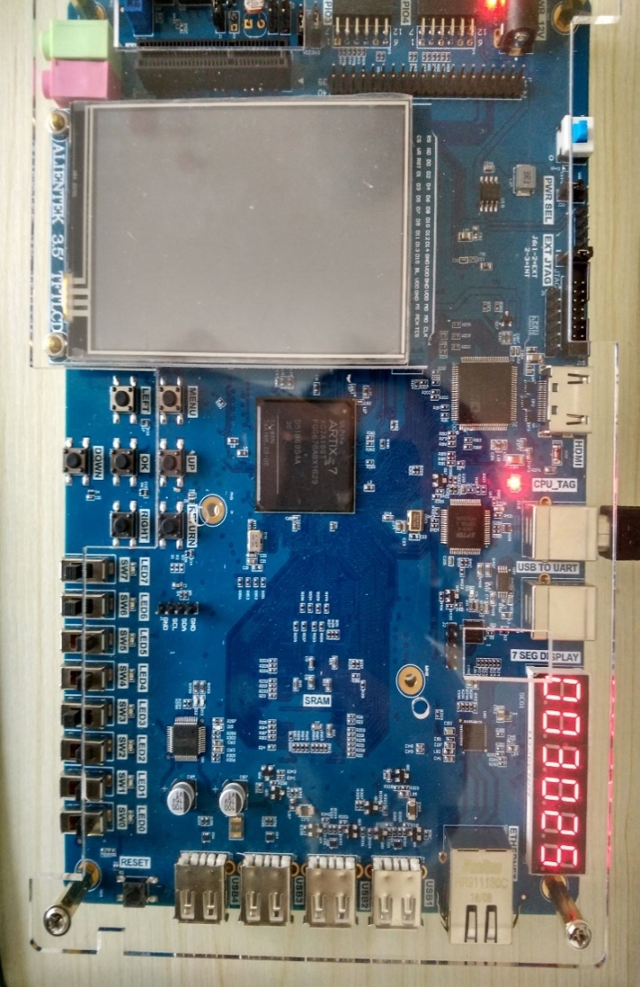
Fig 9. 6 Test result
- Experiment summary and reflection
- How to use the initial file of ROM to realize the decoding, such as decoding and scanning the segment decoders.
- Write a *.mif file to generate sine, cosine wave, and other function generators.
- Comprehend application, combine the characteristic of ROM and PWM to form SPWM modulation waveform.