Block_Debouncing Principle and adaptive programming, PCB schematics, and Verilog HDL Code – FBGA Board for beginner FPGA tutorial – Experiment 5
Experiment 5 Button Debounce Experiment
5.1 Experiment Objective
- Review the design process of the shifting LED
- Learn button debounce principle and adaptive programming
- Study the connection and use of the FII-PRA006/010 button hardware circuit
- Comprehensive application button debounce and other conforming programming
5.2 Experiment Implement
- Control the movement of the lit LED by pressing the button
- Each time the button is pressed, the lit LED moves one bit.
- When the left shift button is pressed, the lit LED moves to the left, presses the right button, and the lit LED moves to the right.
5.3 Experiment
5.3.1 Introduction to Buttons and Debounce Principle
- Introduction to buttons
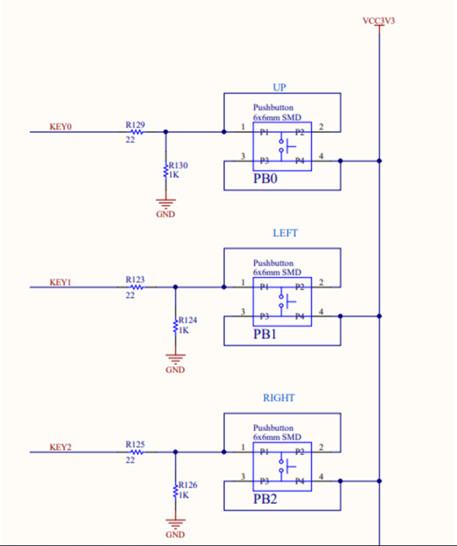
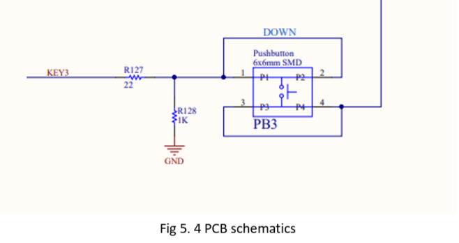
The on-board buttons are common push buttons, which are valid when pressed, and automatically pops up when released. A total of five, respectively, PB0 (UP), PB1 (LEFT), PB2 (RIGHT), PB3(DOWN) and a hardware reset button (RESET). As shown in Figure 5.1.
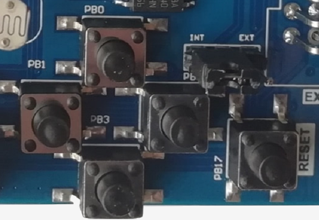
Figure 5.1 Button physical picture
- Principle of button debounce
As long as mechanical buttons are used, instability should be considered. Usually, the switches used for the buttons are mechanical elastic switches. When the mechanical contacts are opened and closed, due to the elastic action of the mechanical contacts, a push button switch does not immediately turn on when closed, nor is it off when disconnected. Instead, there is some bouncing when connecting and disconnecting. See Figure 5.2.
The length of the button’s stable closing time is determined by the operator. It usually takes more than 100ms. If pressing it quickly, it will reach 40-50ms. It is difficult to make it even shorter. The bouncing time is determined by the mechanical characteristics of the button. It is usually between a few milliseconds and tens of milliseconds. To ensure that the program responds to the button’s every on and off, it must be debounced. When the change of the button state is detected, it should not be immediately responding to the action, but waiting for the closure or the disconnection to be stabilized before processing. Button debounce can be divided into hardware debounce and software debounce.
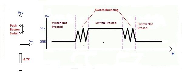
Figure 5.2 Button bounce principle
In most of cases, software or programs are used to achieve debounce. The simplest debounce principle is to wait for a delay time of about 10ms after detecting the change of the button state, and then perform the button state detection again after the bounce disappears. If the state is the same as the previous state just detected, the button can be confirmed. The action has been stabilized. This type of detection is widely used in traditional software design. However, as the number of button usage increases, or the buttons of different qualities will react differently. If the delay is too short, the bounce cannot be filtered out. When the delay is too long, it affects the sensitivity of the button.
5.3.2 Hardware Design
The schematics is shown in Figure 5.3. One side of the button (P1, P2) is connected to VCC, and the other side (P3, P4) is connected to the FPGA. At the same time, it is connected to GND through a 1 kohm resistor. In the normal state, the button is floating, thus the potential of the button P3 is 0, so the input value of the button to the FPGA is 0; when the button is pressed, the buttons are turned on both sides, and the potential of the button P3 is VCC3.3V, so the input value of the button to the FPGA is 1. The onboard switch is active high.
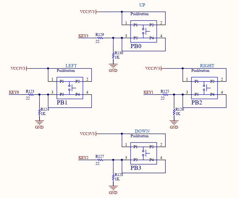
Figure 5.3 Schematics of buttons
5.3.3 Program Design
5.3.3.1 System Block Diagram
Figure 5.4 shows the block diagram of the button controlled shifting LED system.
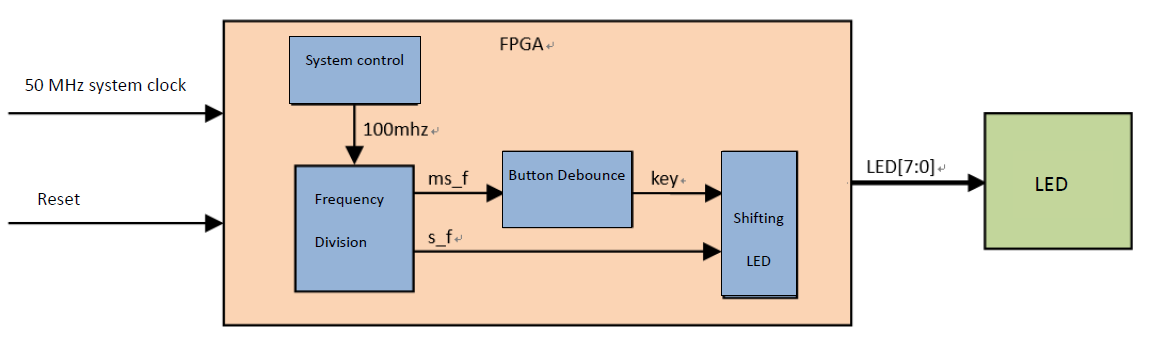
Figure 5.4 System block diagram
The top-level module RTL view is shown in Figure 5.5.
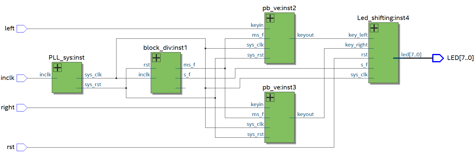
Figure 5.5 RTL view
See Figure 5.6 for the top level design.
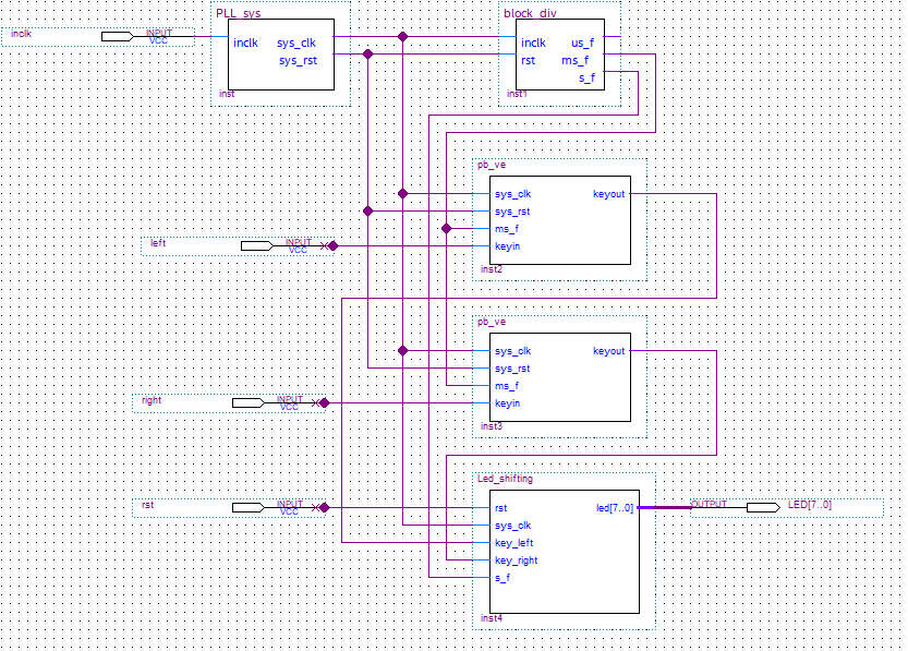
Figure 5.6 Top level design
5.3.3.2 Introduction to the Program
Refer to the previous experiments for the frequency division module and the LED display module. Here, a new part of the button debounce module is introduced.
This chapter introduces an adaptive button debounce method: starts timing when a change in the state of the button is detected. If the state changes within 10ms, the button bouncing exists. It returns to the initial state, clears the delay counter, and re-detects the button state until the delay counter counts to 10ms. The same debounce method is used for pressing and releasing the button. The flow chart is shown in Figure 5.7. Case 0 and 1 debounce the button press state. Case 2 and 3 debounce the button release state. After finishing the whole debounce procedure, the program outputs a synchronized clock pulse.
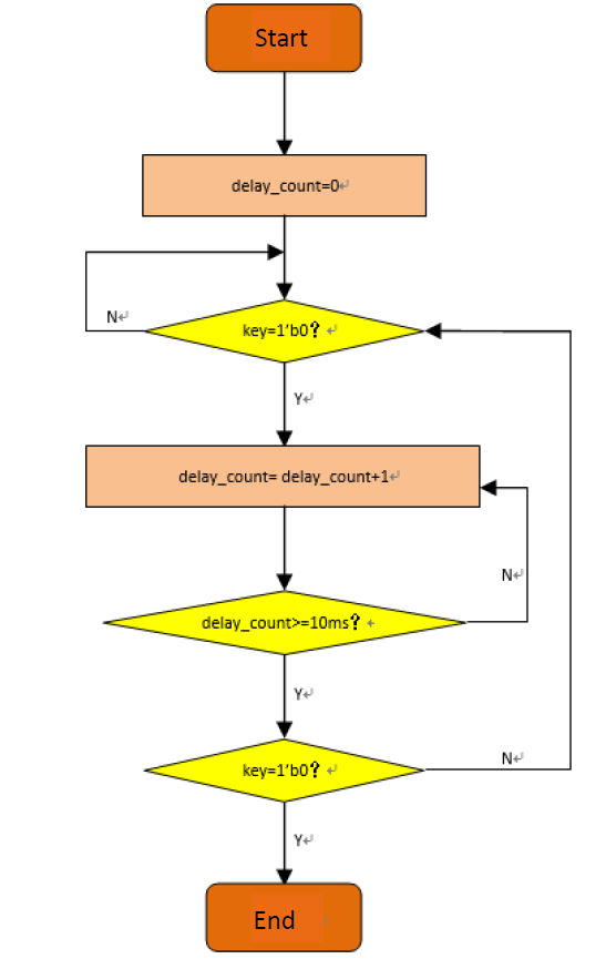
Figure 5.7 Button debounce flow chart
module pb_ve (
input sys_clk,

input sys_rst,

input ms_f,

input keyin,

output keyout

);

reg keyin_r;

reg keyout_r;

reg [1:0] ve_key_st;

reg [3:0] ve_key_count;

always @ (posedge sys_clk)

begin

keyin_r <= keyin;

end

always @ (posedge sys_clk)

begin

if (sys_rst) begin

keyout_r <= 1'b0;

ve_key_count <= 0;

ve_key_st <= 0;

end

else case (ve_key_st)

0 :

begin

keyout_r <= 1'b0;

ve_key_count <= 0;

if (keyin_r)

ve_key_st <= 1;

end

1 :

begin

if (!keyin_r)

ve_key_st <= 0;

else begin

if (ve_key_count == 10)

ve_key_st <= 2;

else if (ms_f)

ve_key_count <= ve_key_count + 1'b1;

end

end

2 :

begin

ve_key_count <= 0;

if (!keyin_r)

ve_key_st <= 3;

end

3 :

begin

if (keyin_r)

ve_key_st <= 2;

else begin

if (ve_key_count == 10) begin

ve_key_st <= 0;

keyout_r <= 1'b1;

end

else if (ms_f)

ve_key_count <= ve_key_count + 1'b1;

end

end

default : ;

endcase

end

assign keyout = keyout_r;

endmodule
5.4 Experiment Verification
The first step: pin assignment
See Table 5.1 for the pin assignment
Table 5.1 Button debounce pin mapping
| Signal Name | Network Label | FPGA Pin | Port Description |
| left | KEY1 | 3 | Left shift signal |
| right | KEY2 | 7 | Right shift signal |
| rst | KEY3 | 10 | Reset |
| led[7] | SW7_LED7 | 77 | LED 7 |
| led[6] | SW6_LED6 | 76 | LED 6 |
| led[5] | SW5_LED5 | 75 | LED 5 |
| led[4] | SW4_LED4 | 74 | LED 4 |
| led[3] | SW3_LED3 | 87 | LED 3 |
| led[2] | SW2_LED2 | 86 | LED 2 |
| led[1] | SW1_LED1 | 83 | LED 1 |
| led[0] | SW0_LED0 | 80 | LED 0 |
The second step: program the development board
After the pin assignment is completed, the compilation is performed. The experimental phenomenon is shown in Figure 5.8 to Figure 5.10 below.
After the development board is programmed, the LEDs are completely off, press the reset button, the LED are fully illuminated, as shown in Figure 5.8.
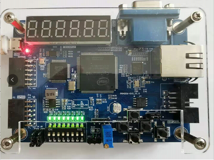
Figure 5.8 Button debounce experiment phenomenon (Reset state)
When the right shift button is pressed, the highest LED lights up. See Figure 5.9.
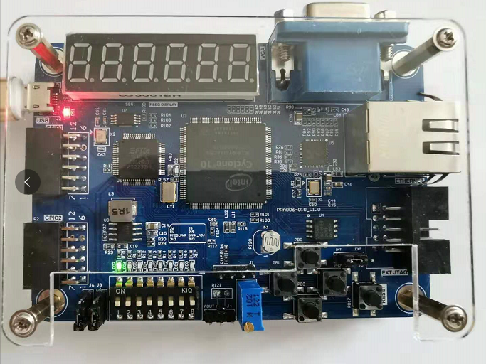
Figure 5. 9 Button debounce experiment phenomenon (One right shift)
Press the right shift button again and the LED will move one bit to the right. See Figure 5.10.
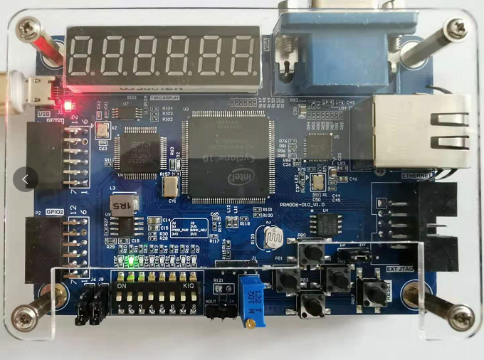
Figure 5. 10 Button debounce experiment phenomenon (Another right shift)
Old version (2019 )
5.1 Experiment Objective
- Review the design process of running LED
- Learn the principle of button debounce and designing of adaptive programming
- Learn the connection and used of the Fii-PRA010 button
- Integrated application of button debounce, and furthermore development design
5.2 Experiment
- Bouncing button principle
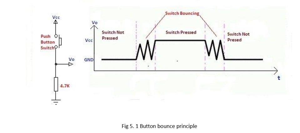
Usually, the switches used for the buttons are mechanical elastic switches. When the mechanical contacts are opened and closed, due to the elastic action of the mechanical contacts, a push button switch does not immediately turn on when closed, nor is it off when disconnected. Instead, there is some bouncing when connecting and disconnecting. See Fig 5. 1
The length of the button’s stable closing time is determined by the operator. It usually takes more than 100ms. If you press it quickly, it will reach 40-50ms. It is difficult to make it even shorter. The bouncing time is determined by the mechanical characteristics of the button. It is usually between a few milliseconds and tens of milliseconds. To ensure that the program responds to the button’s every on and off, it must be debounced. When the change of the button state is detected, it should not be immediately responding to the action, but waiting for the closure or the disconnection to be stabilized before processing. Button debounce can be divided into hardware debounce and software debounce.
In most of cases, we use software or programs to achieve debounce. The simplest debounce principle is to wait for a delay time of about 10ms after detecting the change of the button state, and then perform the button state detection again after the bounce disappears. If the state is the same as the previous state just detected, the button can be confirmed. The action has been stabilized. This type of detection is widely used in traditional software design. However, as the number of button usage increases, or the buttons of different qualities will react differently. If the delay is too short, the bounce cannot be filtered out. When the delay is too long, it affects the sensitivity of the button.
This chapter introduces an adaptive button debounce method: starts timing when a change in the state of the button is detected. If the state changes within 10ms, the button bouncing exists. It returns to the initial state, clears the delay counter, and re-detects the button state until the delay counter counts to 10ms. The same debounce method is used for pressing and releasing the button.
The flow chart is shown in Fig 5. 2.
- Code for button debouncing
Verilog code is as follows:
module pb_ve( input sys_clk, // 100 Mhz input sys_rst, // input ms_f, // input keyin, // <span lang="en-CA">Input status of the key</span> output keyout //Output status of key. Every time releasing the button, only one system //clock pulse outputs ); reg keyin_r; //Input latch to eliminate metastable reg keyout_r;// //push_button vibrating elemination reg [1:0] ve_key_st; //State machine status bit reg [3:0] ve_key_count; //delay counter always@(posedge sys_clk) keyin_r<=keyin; // Input latch to eliminate metastable always@(posedge sys_clk) if(sys_rst) begin keyout_r <=1'b0; ve_key_count <=0; ve_key_st <=0; end else case(ve_key_st) 0:begin keyout_r<=1'b0; ve_key_count <=0; if(keyin_r) ve_key_st <=1; end 1:begin if(!keyin_r) ve_key_st <=0; else begin if(ve_key_count==10) begin ve_key_st <=2; end else if(ms_f) ve_key_count<=ve_key_count+1; end end 2:begin ve_key_count <=0; if(!keyin_r) ve_key_st <=3; end 3:begin if(keyin_r) ve_key_st <=2; else begin if(ve_key_count==10) begin ve_key_st <=0; keyout_r<=1'b1; //After releasing debounce, output a //synchronized clock pulse end else if(ms_f) ve_key_count<=ve_key_count+1; end end default:; endcase assign keyout=keyout_r; endmodule
Case 0 and 1 debounce the button press state. Case 2 and 3 debounce the button release state. After finishing the whole debounce procedure, the program outputs a synchronized clock pulse.
-
Button debounce flow chart
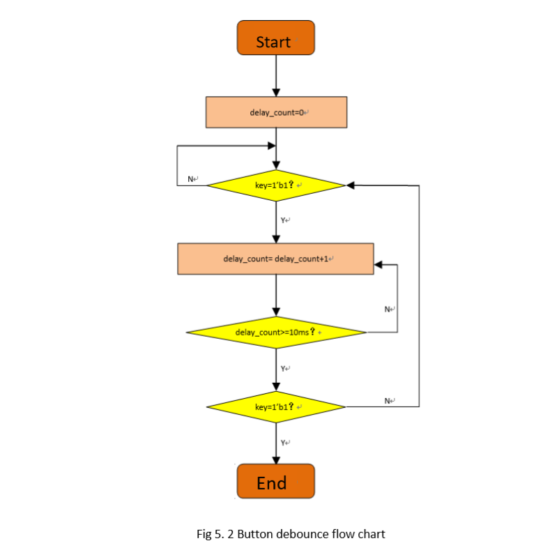
Fig 5. 2 Button debounce flow chart
- Combine running LED design and modify the button debounce.
-
- Build new project
- Create a PLL symbol
- Create a button debounce symbol (See the Verilog HDL code in this experiment)
- Create a running LED symbol
//Verilog code
</pre>
module Led_shifting(

input rst,

input sys_clk,

input key_left,

input key_right,

input s_f,

output reg [7:0] led

);

reg ext_rst;

always@(posedge sys_clk) begin

ext_rst<=rst;

end

always@(posedge sys_clk)

if(ext_rst)begin

led<=8'hff;

end

else begin

if(key_left) begin

if(led==8'hff)

led<=8'b0000_0001;

else

led<={led[6:0],led[7]};

end

else if(key_right) begin

if(led==8'hff)

led<=8'b1000_0000;

else

led<={led[0],led[7:1]};

end

end

endmodule
-
-
Create top level file and combine each symbol referring to Experiment 4. See Fig 5. 3
-
Pin assignment
-
|
Signal Name |
Port Description |
Network Label |
FPGA Pin |
|
left |
Left shift signal |
KEY0 |
3 |
|
right |
Right shift signal |
KEY1 |
7 |
|
rst |
Reset signal |
KEY2 |
10 |
Table 5. 1 Pin assignment
One more thing to mention is that in the I/O Standard column, select 3.3-V LVCMOS instead of 2.5 V
g. Compile
h. Download the program to the board
i. Observe the testing result, to see whether every time pressing a button, LED will move towards the corresponding direction. PB3 is reset, PB1 is to move to the left, and PB2 is to move to the right. (block_debouncing Quartus II project files can be referred).
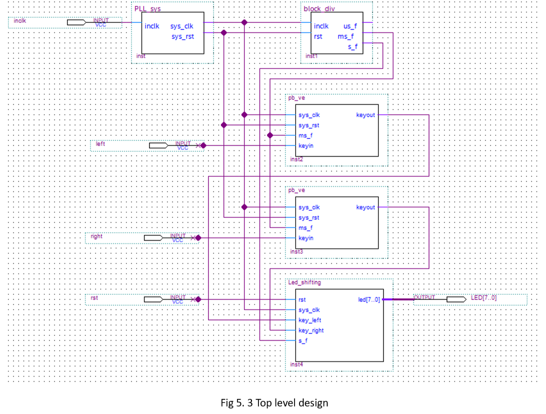
Fig 5. 3 Top level design
Button PCB schematics. See Fig 5. 4