Description
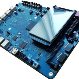
FII-PE7030 Development and Experiment Board
It is out of Stock
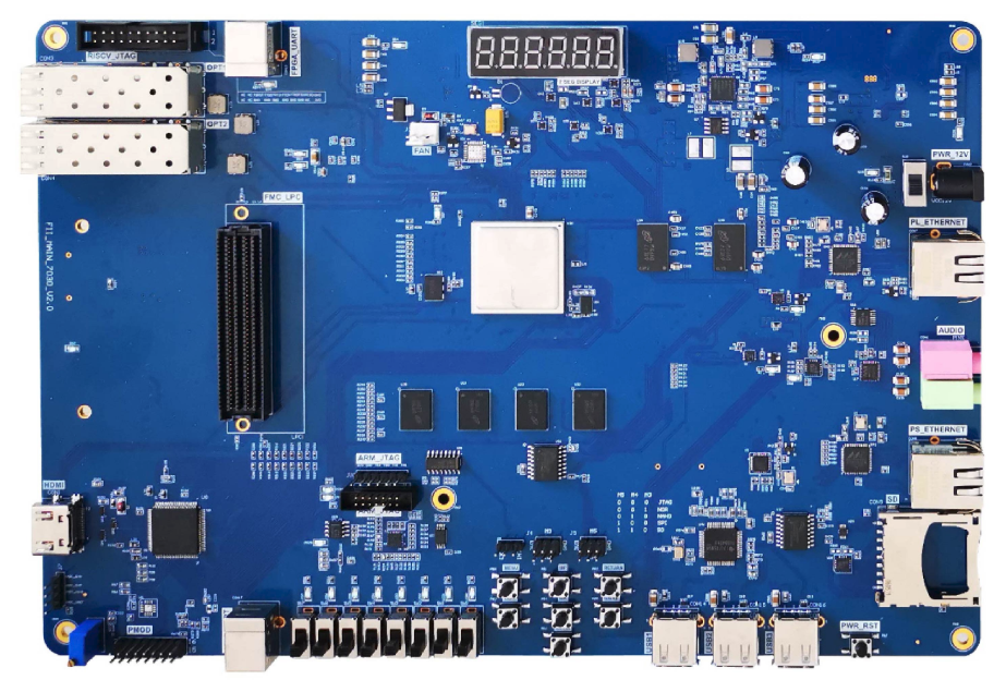
Basic Experiment Functions:
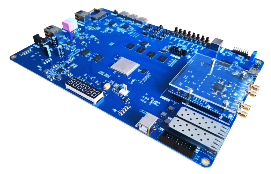
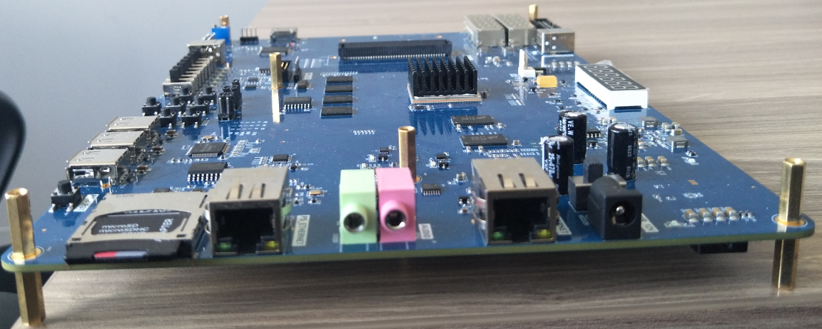
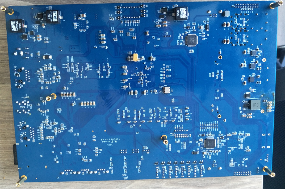
FII-PE7030 is a ready-to-use for educational platform which has been designed to cover FPGA development and experiment, ARM SOC development and experiment, network(copper or fiber) development, digital communication and SDR(software define radio) with daughter board FII-BD9361 plug on. It was designed for university students, teachers, and all other industrail professionals. FII-PE7030 is an incredibly flexible processing platform, capable of adapting to most of your project requires.
More surprising show up that recently Engineers has successful port RISC-V(RV32G) and RV64I to this platform, it becomes a real RISC-V SOC platform.
Application:
wireless Communication
DBC(digital base band communication) and DSP
SDR Software defined radio
LTE protocol analysis
4/5G base station
Network communication:
100M/1G ethernet communication both for PS and PL
10G SFP+ fibre communication with multiple protocol supported like LAN, SONET/SDH, CPRI etc.
Network switch and router
VLAN
Spanning Tree
USB:
1 480M high speed USB2.0 HUB
4 480M high speed USB2.0 connectors
CPU:
RISC-V CPU 32bit ecosystem development ,verification and validation
RISC-V CPU 64bit ecosystem development,verification and validation
Artificial Intelligence:
Audio or Voice Collection, Speech Recognition
Image Acquisition and Image Recognition, Deep Learning
IOT: ALL kinds of IOTs with RISC-V system
FII-PE7030 System Hardware Resources:
- 2 ports 10G Ethernet(Fibre)
- 2 ports100M/1G Ethernet, one for PS and for PL
- 1 HDMI output Interface。
- dual channel Audio Interface
- AD9361 Interface(FMC-LPC)
- 8 LEDs
- 8 switches
- 8 buttons
- GPIO Expansion Port
- JTAG Debug Interface
- 1GB ddr3 –SOC(PS)
- 1GB ddr3—FPGA(PL)
- SDCARD Interface
- 32M Serial FLASH
- Serial EEPROM
- 12bit 1MPS ADC
- Temperature Sensor

- FII-PE7030 Hardware Reference Guide
- EVB Board – FII-PE7030 User Experimental Manuals
- Introduction to Zynq_7030 Development System FII-PE7030
- zynq_7030 Main Resources Usage and FPGA Development Experiemnt
- zynq xc7z030 board – FII-PE7030 Experiment 1 LED Shifting Design
- zynq xc7z030 board – FII-PE7030 Experiment 2 – Analysis of Switch Signals via ILA
- zynq xc7z030 board – FII-PE7030 Experiment 3 – Segment Display Digital Clock Experiment
- zynq xc7z030 board – FII-PE7030 Experiment 4 – Button Debounce
- zynq xc7z030 board – FII-PE7030 Experiment 5 – Digital Clock Comprehensive Experiment
- zynq xc7z030 board – FII-PE7030 Experiment 6 – Use of Multipliers and ISIM
- zynq xc7z030 board – FII-PE7030 Experiment 7 – Hexadecimal Number to BCD Code Conversion and Application
- zynq xc7z030 board – FII-PE7030 Experiment 8 – Use of ROM
- zynq xc7z030 board – FII-PE7030 Experiment 9 – Use Dual-port RAM to Read and Write Frame Data
- zynq xc7z030 board – FII-PE7030 Experiment 10 – Asynchronous Serial Port Design and Experiment
- zynq xc7z030 board – FII-PE7030 Experiment 11 – IIC Protocol Transmission
- zynq xc7z030 board – FII-PE7030 Experiment 12 – HDMI Experiment
- zynq xc7z030 board – FII-PE7030 Experiment 13 – Ethernet Experiment
If you have any questions, you can contact me online. You can also post your questions in our FII-PE7030 forums
For User Experimental Manuals, please click
FII-PE7030 FPGA Development Board and Educational Platform Experimental Manual and Haredware Reference Guide
We will send you the newest Document and project files after you have ordered the products from us.
PE7030 hardware reference guide
PE7030 hardware reference guidezynq_7030_evb_SCH_20190816_NP
For



Reviews
There are no reviews yet.