IIC protocol knowledge,Learn HDMI theory – zynq xc7z030 board – FII-PE7030 Experiment 12 – HDMI Experiment
Experiment 12 HDMI Experiment
12.1 Experiment Objective
- Review IIC protocol knowledge
- Learn HDMI theory
12.2 Experiment Implement
Through the HDMI interface, different image contents are displayed on the screen.
12.3 Experiment
12.3.1 Introduction to HDMI Interface and ADV7511 Chip
Image display processing has always been the focus of FPGA research. At present, the image display mode is also developing. The image display interface is also gradually transitioning from the old VGA interface to the new DVI or HDMI interface. HDMI (High Definition Multimedia Interface) is a digital video/audio interface technology. It is a dedicated digital interface for image transmission. It can transmit audio and video signals at the same time.
The ADV7511 is a chip that converts FPGA digital signal to HDMI signal following VESA standard. For more details, see the related chip manual. Among them, “ADV7511 Programming Guide” and “ADV7511 Hardware Users Guide” are the most important. The registers of the ADV7511 can be configured by referring those documents.
ADV7511 Register Configuration Description: The bus inputs D0-D3, D12-D15, and D24-D27 of the ADV7511 have no input, and each bit of data is in 8-bit mode. Directly set 0x15 [3:0]) 0x0 data, 0x16 [3:2] data does not need to be set for its mode. Set [5:4] of 0X16 to 11for 8-bit data and keep the default values for the other digits. 0x17[1] refers to the ratio of the length to the width of the image. It can be set to 0 or 1. The actual LCD screen will not change according to the data, but will automatically stretch the full screen mode according to the LCD’s own settings. 0x18[7] is the way to start the color range stretching. The design is that RGB maps directly to RGB, so it can be disabled directly. 0X18[6:5] is also invalid currently. 0XAF[1] is to set HDMI or DVI mode, the most direct point of HDMI than DVI is that HDMI can send digital audio data and encrypted data content. This experiment only needs to display the picture, and it can be set directly to DVI mode. Set 0XAF[7] to 0 to turn off HDMI encryption. Due to GCCD, deep color encryption data is not applicable, so the GC option is turned off. 0x4c register does not need to be set as well. Other sound data setting can be ignored here for DVI output mode. After writing these registers, the image can be displayed successfully.
12.3.2 Hardware Design
The onboard HDMI module consists of an HDMI interface and an ADV7511 chip. The actual picture is shown in Figure 12.1. The schematic is shown in Figure 12.2.
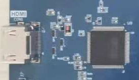
Figure 12.1 Physical picture of HDMI interface and ADV7511 chip
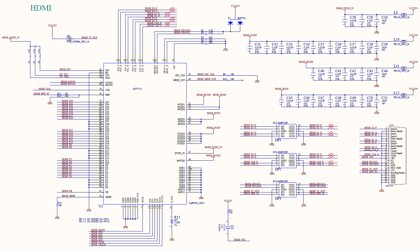
Figure 12.2 Schematics of HDMI
ADV7511 chip is set through the IIC bus and send the picture information to be displayed to the chip through HDMI_D0 to HDMI_D23, and control signals HDMI_HSYNC and HDMI_VSYNC and the clock signal HDMI_CLK, which are transmitted to the PC through the HDMI interface after being processed internally by the chip.
12.3.3 Program Introduction
The configuration part of the ADV7511 chip is carried out using the IIC protocol, with reference to Experiment 11 and Experiment 12. A brief introduction to the data processing section is now available.
| module hdmi_test (
input inclk_p, input inclk_n, input rst, input key1, output rgb_hs, output rgb_vs, output [7:0] rgb_r, output [7:0] rgb_g, output [7:0] rgb_b, output rgb_clk, inout scl, inout sda, output en ); endmodule |
FPGA configures the ADV7511 chip through the IIC bus (clock line scl, data line sda). After the configuration is complete, the output image information needs to be determined. Taking the 1080P (1920 * 1080) image format as an example, the data signals rgb_r (red component), rgb_g (green component), rgb_b (blue component), line synchronization signal rgb_hs, field synchronization signal rgb_vs, and a clock rgb_clk will be output. Each pixel is formed by a combination of three color components. Each row of 1920 pixels is filled with color information in a certain order (from left to right). After one line is completed, the next line is completed in a certain order (from top to bottom) until 1080 lines have been finihsed, so one frame of image information is completed. The image information of each frame is determined by this horizontal and vertical scanning, and then transmitted to the ADV7511 for processing. The timing diagrams of horizontal and vertical scanning are shown in Figures 12.3 and 12.4.
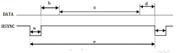
Figure 12.3 Horizontal synchronization
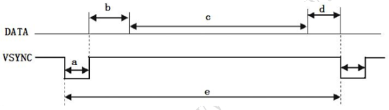
Figure 12.4 Vertical synchronization
The second step: data definition of 1080p image timing generation
| Horizontal line scan parameter setting 1920*1080@60 Hz clock 130 MHz
parameter LinePeriod = 2000; //Line period parameter H_SyncPulse = 12; //Line sync pulse (Sync a) parameter H_BackPorch = 40; //Display back edge (Back porch b) parameter H_ActivePix = 1920; // Display timing (Display interval c) parameter H_FrontPorch= 28; //Display front edge (Front porch d) parameter Hde_start = 52; parameter Hde_end = 1972; Vertical scan parameter setting 1920*1080@60Hz parameter FramePeriod = 1105; //Frame period parameter V_SyncPulse = 4; //Vertical sync pulse (Sync o) parameter V_BackPorch = 18; //Display trailing edge (Back porch p) parameter V_ActivePix = 1080; //Display timing (Display interval q) parameter V_FrontPorch= 3; //Display front edge (Front porch r) parameter Vde_start = 22; parameter Vde_end = 1102;
reg [12:0] x_cnt; reg [10:0] y_cnt; reg [23:0] grid_data_1; reg [23:0] grid_data_2; reg [23:0] bar_data; reg [3:0] rgb_dis_mode; reg [7:0 ] rgb_r_reg; reg [7:0] rgb_g_reg; reg [7:0] rgb_b_reg; reg hsync_r; reg vsync_r; reg hsync_de; reg vsync_de; reg [15:0] key1_counter; //pushu button
wire locked; reg rst; wire [12:0] bar_interval;
assign bar_interval = H_ActivePix[15: 3]; //Color strip width |
The third step: generate display content
| always @ (posedge rgb_clk)
begin if (rst) hsync_r <= 1’b1; else if (x_cnt == LinePeriod) hsync_r <= 1’b0; else if (x_cnt == H_SyncPulse) hsync_r <= 1’b1; if (rst) hsync_de <= 1’b0; else if (x_cnt == Hde_start) hsync_de <= 1’b1; else if (x_cnt == Hde_end) hsync_de <= 1’b0; end always @ (posedge rgb_clk) begin if (rst) y_cnt <= 1’b1; else if (x_cnt == LinePeriod) begin if (y_cnt == FramePeriod) y_cnt <= 1’b1; else y_cnt <= y_cnt + 1’b1; end end always @ (posedge rgb_clk) begin if (rst) vsync_r <= 1’b1; else if ((y_cnt == FramePeriod) &(x_cnt == LinePeriod)) vsync_r <= 1’b0; else if ((y_cnt == V_SyncPulse) &(x_cnt == LinePeriod)) vsync_r <= 1’b1; if (rst) vsync_de <= 1’b0; else if ((y_cnt == Vde_start) & (x_cnt == LinePeriod)) vsync_de <= 1’b1; else if ((y_cnt == Vde_end) & (x_cnt == LinePeriod)) vsync_de <= 1’b0; end assign en = hsync_de & vsync_de; always @(posedge rgb_clk) begin if ((x_cnt[4]==1’b1) ^ (y_cnt[4]==1’b1)) grid_data_1 <= 24’h000000; else grid_data_1<= 24’hffffff; if ((x_cnt[6] == 1’b1) ^ (y_cnt[6] == 1’b1)) grid_data_2 <=24’h000000; else grid_data_2 <=24’hffffff; end always @ (posedge rgb _clk) begin if (x_cnt==Hde_start) bar_data <= 24’hff0000; //Red strip else if (x_cnt == Hde_start + bar_interval) bar_data <= 24’h00ff00; //Green strip else if (x_cnt == Hde_start + bar_interval*2) bar_data <= 24’h0000ff; //Blue strip else if (x_cnt == Hde_start + bar_interval*3) bar_data <= 24’hff00ff; //Purple strip else if (x_cnt == Hde_start + bar_interval*4) bar_data <= 24’hffff00; //Yellow strip else if (x_cnt == Hde_start + bar_interval*5) bar_data <= 24’h00ffff; //Light blue strip else if (x_cnt == Hde_start + bar_interval*6) bar_data <= 24’hffffff; //White strip else if (x_cnt == Hde_start + bar_interval*7) bar_data <= 24’hff8000; //Orange strip else if (x_cnt == Hde_start + bar_interval*8) bar_data <= 24’h000000; //Black strip end always @ (posedge rgb_clk) begin if (rst) begin rgb_r_reg <= 0; rgb_g_reg <= 0; rgb_b_reg <= 0; end else case (rgb_dis_mode) 4’b0000 : //Display all black begin rgb_r_reg <= 0; rgb_g_reg <= 0; rgb_b_reg <= 0; end 4’b0001 : //Display all white begin rgb_r_reg <= 8’hff; rgb_g_reg <= 8’hff; rgb_b_reg <= 8’hff; end 4’b0010 : //Display all red begin rgb_r_reg <= 8’hff; rgb_g_reg <= 0; rgb_b_reg <= 0; end 4’b0011 : //Display all green begin rgb_r_reg <= 0; rgb_g_reg <= 8’hff; rgb_b_reg <= 0; end 4’b0100 : //Display all blue begin rgb_r_reg <= 0; rgb_g_reg <= 0; rgb_b_reg <= 8’hff; end 4’b0101 : // Display square 1 begin rgb_r_reg <= grid_data_1[23:16]; rgb_g_reg <= grid_data_1[15:8]; rgb_b_reg <= grid_data_1[7:0]; end 4’b0110 : // Display square 2 begin rgb_r_reg <= grid_data_2[23:16]; rgb_g_reg <= grid_data_2[15:8]; rgb_b_reg <= grid_data_2[7:0]; end 4’b0111 : // Display horizontal gradient begin rgb_r_reg <= x_cnt[10:3]; rgb_g_reg <= x_cnt[10:3]; rgb_b_reg <= x_cnt[10:3]; end 4’b1000 : // Display vertical gradient begin rgb_r_reg <= y_cnt[10:3]; rgb_g_reg <= y_cnt[10:3]; rgb_b_reg <= y_cnt[10:3]; end 4’b1001 : // Display red horizontal gradient begin rgb_r_reg <= x_cnt[10:3]; rgb_g_reg <= 0; rgb_b_reg <= 0; end 4’b1010 : // Display green horizontal gradient begin rgb_r_reg <= 0; rgb_g_reg <= x_cnt[10:3]; rgb_b_reg <= 0; end 4’b1011 : // Display blue horizontal gradient begin rgb_r_reg <= 0; rgb_g_reg <= 0; rgb_b_reg <= x_cnt[10:3]; end 4’b1100 : // Display colorful strips begin rgb_r_reg <= bar_data[23:16]; rgb_g_reg <= bar_data[15:8]; rgb_b_reg <= bar_data[7:0]; end default : // Display all white begin rgb_r_reg <= 8’hff; rgb_g_reg <= 8’hff; rgb_b_reg <= 8’hff; end endcase end assign rgb_hs = hsync_r; assign rgb_vs = vsync_r; assign rgb_r = (hsync_de & vsync_de) ? rgb_r_reg : 8’h00; assign rgb_g = (hsync_de & vsync_de) ? rgb_g_reg : 8’b00; assign rgb_b = (hsync_de & vsync_de) ? rgb_b_reg : 8’h00;
always @(posedge rgb_clk) begin if (key1 == 1’b1) key1_counter <= 0; else if ((key1 == 1’b0) & (key1_counter <= 16’d130000)) key1_counter <= key1_counter + 1’b1; if (key1_counter == 16’h129999) begin if(rgb_dis_mode == 4’b1100) rgb_dis_mode <= 4’b0000; else rgb_dis_mode <= rgb_dis_mode + 1’b1; end end |
When the push button is pressed, a key1 signal will be input, and the content displayed on the screen will change according to the change of vga_dis_mode, and the corresponding picture content will be displayed.
12.4 Experiment Verification
The first step: assign the pins
The pin assignment is shown in Table 12.1.
Table 12.1 HDMI experiment pin mapping table
| Signal Name | Network Name | FPGA Pin | Port Description |
| inclk_p | SYSCLK_P | AC13 | Input clock (differential)
200MHz |
| inclk_n | SYSCLK_N | AD13 | |
| rst | GPIO_SW_2 | F4 | Reset button |
| key1 | GPIO_SW_1 | G4 | Mode switching button |
| scl | IIC_SCL_MAIN_LS | W14 | IIC clock bus |
| sda | IIC_SDA_MAIN_LS | W17 | IIC data bus |
| rgb_clk | HDMI_R_CLK | AD19 | HDMI image clock |
| en | HDMI_R_DE | AE25 | HDMI image enable signal |
| rgb_hs | HDMI_R_HS | AA22 | Horizontal sync signal |
| rgb_vs | HDMI_R_VS | AE18 | Vertical sync signal |
| rgb_b[0] | HDMI_R_D0 | AD18 | Image blue output |
| rgb_b[1] | HDMI_R_D1 | AC18 | |
| rgb_b[2] | HDMI_R_D2 | AE26 | |
| rgb_b[3] | HDMI_R_D3 | AC21 | |
| rgb_b[4] | HDMI_R_D4 | AE23 | |
| rgb_b[5] | HDMI_R_D5 | AC22 | |
| rgb_b[6] | HDMI_R_D6 | AD25 | |
| rgb_b[7] | HDMI_R_D7 | AF19 | |
| rgb_g[0] | HDMI_R_D8 | AF24 | Image green output |
| rgb_g[1] | HDMI_R_D9 | AD26 | |
| rgb_g[2] | HDMI_R_D10 | AF20 | |
| rgb_g[3] | HDMI_R_D11 | AD23 | |
| rgb_g[4] | HDMI_R_D12 | AE20 | |
| rgb_g[5] | HDMI_R_D13 | AA23 | |
| rgb_g[6] | HDMI_R_D14 | AC19 | |
| rgb_g[7] | HDMI_R_D15 | AF25 | |
| rgb_r[0] | HDMI_R_D16 | AB19 | Image red output |
| rgb_r[1] | HDMI_R_D17 | AB24 | |
| rgb_r[2] | HDMI_R_D18 | AA19 | |
| rgb_r[3] | HDMI_R_D19 | AB21 | |
| rgb_r[4] | HDMI_R_D20 | AB20 | |
| rgb_r[5] | HDMI_R_D21 | AA24 | |
| rgb_r[6] | HDMI_R_D22 | W19 | |
| rgb_r[7] | HDMI_R_D23 | AB22 |
The second step: run the implementation, generate bitstream files, and verify the board
Download the generated programmable bitstream file to the Zynq_7030 development board. Press the switch button and the display content changes accordingly. The phenomenon is shown in the following figure. (List only a few)
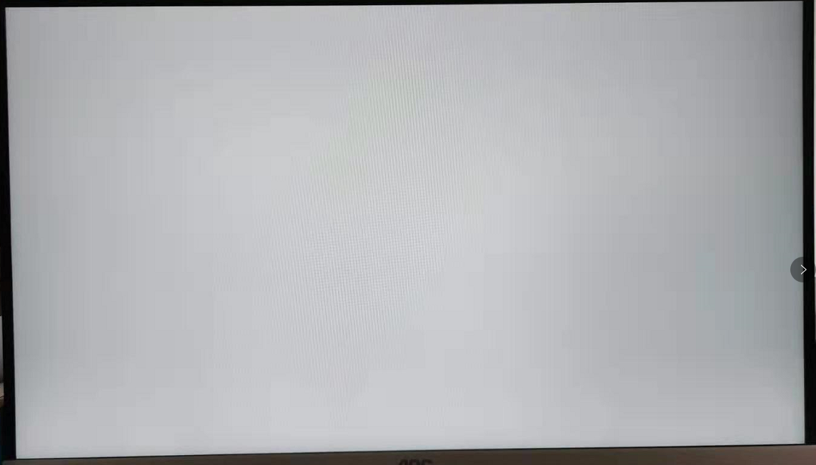
Figure 12.5 HDMI display (all white)
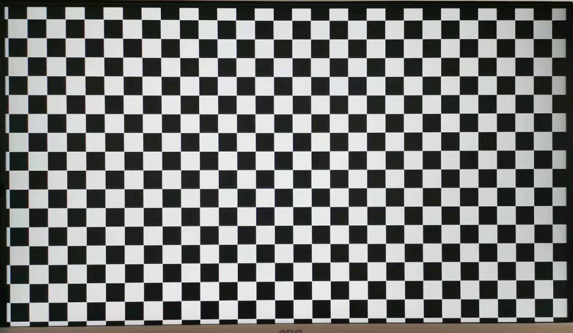
Figure 12.6 HDMI display (square)
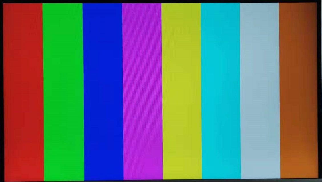
Figure 12.7 HDMI display (color strip)