asynchronous IIC bus, and the IIC communication protocol, reading and writing EEPROM – zynq xc7z030 board – FII-PE7030 Experiment 11 – IIC Protocol Transmission
Experiment 11 IIC Protocol Transmission
11.1 Experiment Objective
- Learning the basic principles of asynchronous IIC bus, and the IIC communication protocol
- Master the method of reading and writing EEPROM
- Joint debugging using logic analyzer
11.2 Experiment Implement
- Correctly write a number to any address in the EEPROM (this experiment writes to the register of 8’h03 address) through the FPGA (here changes the written 8-bit data value by (SW7~SW0)). After writing in successfully, read the data as well. The read data is displayed directly on the segment display.
- Download the program into the FPGA and press the left push button to execute the data write into EEPROM operation. Press the right push button to read the data that was just written.
- Determine whether it is correct or not by reading the displayed number on the segment display. If the segment display has the same value as written value, the experiment is successful.
- Analyze the correctness of the internal data with ILA and verify it with the display of the segment display.
11.3.1 Introduction to EEPROM and IIC Protocol
- EEPROM Introduction
EEPROM (Electrically Erasable Programmable Read Only M emory) refers to a charged erasable programmable read only register. It is a memory chip that does not lose data after turning off power.
On the experiment board, there is an IIC interface EEPROM chip M24C08 with a capacity of 1024 bytes. Users can store some hardware configuration data or user information due to the characteristics that the data is not lost after power-off.
- The overall timing protocol of IIC is as follows:
- Bus idle state: SDA, SCL are high
- Start of IIC protocol: SCL stays high, SDA jumps from high level to low level, generating a start signal
- IIC read and write data stage: including serial input and output of data and response signal issued by data receiver
- IIC transmission end bit: SCL is in high level, SDA jumps from low level to high level, and generates an end flag. See Figure 11.1.
- SDA must remain unchanged when SCL is high. It changes only when SCL is low
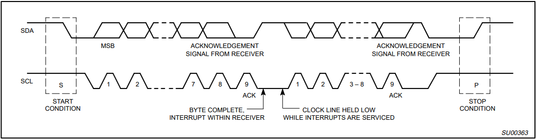
Figure 11.1 Timing protocol of IIC
11.3.2 Hardware Introduction
Each IIC device has a device address. When some device addresses are shipped from the factory, they are fixed by the manufacturer (the specific data can be found in the manufacturer’s data sheet). Some of their higher bits are determined, and the lower bits can be configured by the user according to the requirement. The higher four-bit address of the EEPROM chip M24C08 used by the develop board has been fixed to 1010 by the component manufacturer. The lower three bits are linked in the develop board as shown below, so the device address is 1010000. See Figure 11.2.
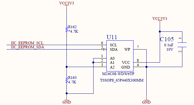
Figure 11.2 IIC schematics EEPROM part
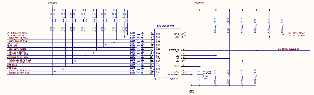
Figure 11.3 IIC SWITCH schematics
EEPROM reads and writes data through the IIC_EEPROM_SCL clock line and the IIC_EEPROM_SDA data line with the FPGA.
Because there are many on-board IIC devices, to save I / O resources of FPGA, PCA9548 chip is used as IIC SWITCH, as shown in Figure 11.3. The FPGA uses IIC_SCL_MAIN and IIC_SDA_MAIN as IIC buses to connect to PCA9548, and then passes PCA9548 to drive IIC devices. It can drive up to 8 IIC devices at the same time and itself is driven by the IIC protocol.
11.3.3 Program Introduction
This experiment has two main modules, I2C reading and writing module and LED display module; The first module is mainly introduced here.
The first step: establishment of the main program framework
| eeprom_test(
input inclk_p, input inclk_n, input rst, input key_wr, input key_rd, input [7:0] sw, output tube_sel1, output tube_sel2, output [7:0] tube_seg, inout scl, inout sda ); |
Inputs are differential clock, reset signal rst, write control signal key_wr, read control signal key_rd, and write content are controlled by switch SW. The output signals are two segment display selection signals tube_sel1, tube_sel2, segment selection signal tube_seg, and a set of IIC bus scl clock lines and sda data lines.
The second step: create clock IIC_CLK
| reg [2:0] cnt;
reg [8:0] cnt_delay; reg scl_r; reg scl_link ; always @ (posedge clk or posedge rst) begin if (rst) cnt_delay <= 9’d0; else if (cnt_delay == 9’d499) cnt_delay <= 9’d0; else cnt_delay <= cnt_delay + 1’b1; //10us end always @ (posedge clk or posedge rst) begin if (rst) cnt <= 3’d5; else begin case (cnt_delay) 9’d124: cnt <= 3’d1; //cnt=1:scl 9’d249: cnt <= 3’d2; //cnt=2:scl 9’d374: cnt <= 3’d3; //cnt=3:scl 9’d499: cnt <= 3’d0; //cnt=0:scl default: cnt<=3’d5; endcase end end `define SCL_POS (cnt==3’d0) //cnt=0:scl `define SCL_HIG (cnt==3’d1) //cnt=1:scl `define SCL_NEG (cnt==3’d2) //cnt=2:scl `define SCL_LOW (cnt==3’d3) //cnt=3:scl always @ (posedge clk or posedge rst) begin if (rst) scl_r <= 1’b0; else if (cnt == 3’d0) scl_r <= 1’b1; else if (cnt == 3’d2) scl_r <= 1’b0; end assign scl = scl_link ? scl_r : 1’bz; |
First, divide 50MHz system clock to obtain a 100KHz clock with a period of 10us as the transmission clock of the I2C protocol, and then use the counter to define the rising edge, high state, falling edge and low state of the clock to prepare for subsequent data reading and writing and the start and end of the I2C protocol. The last sentence means to define a data valid signal. Only when the signal is high, that is, when the data is valid, the I2C clock is valid again, otherwise it is in a high impedance state. This is also set in accordance with the I2C transmission protocol.
The third step: specific implementation of I2C transmission
| `define DEVICE_READ 8’b1010_0001
`define DEVICE_WRITE 8’b1010_0000 `define BYTE_ADDR 8’b0000_0011 `define IIC_SWITCH_ADDR 7’b1110_000 `define EEPROM_CHANNEL 8’b0000_0001 parameter IDLE = 5’d0; parameter START0 = 5’d1; parameter ADD0 = 5’d2; parameter ACK0 = 5’d3; parameter CHANNEL = 5’d4; parameter ACK_C = 5’d5; parameter STOP0 = 5’d6; parameter START1 = 5’d7; parameter ADD1 = 5’d8; parameter ACK1 = 5’d9; parameter ADD2 = 5’d10; parameter ACK2 = 5’d11; parameter START2 = 5’d12; parameter ADD3 = 5’d13; parameter ACK3 = 5’d14; parameter DATA = 5’d15; parameter ACK4 = 5’d16; parameter STOP1 = 5’d17; parameter STOP2 = 5’d18; always @ (posedge clk or posedge rst) begin if (rst) begin cstate <= IDLE; sda_r <= 1’b1; scl_link <= 1’b1; sda_link <= 1’b1; num <= 4’d0; read_data <= 8’b0000_0000; cnt_5ms <= 20’h00000; iic_done <= 1’b0; end else case (cstate) IDLE : begin sda_link <= 1’b1; scl_link <= 1’b1; iic_done <= 1’b0 ; if (wr_en) begin db_r <= {`IIC_SWITCH_ADDR, 1’b0}; cstate <= START0; end else if (rd_en) begin db_r <= {`IIC_SWITCH_ADDR, 1’b1}; cstate <= START0; end else cstate <= IDLE; end START0 : begin if (`SCL_HIG) begin sda_link <= 1’b1; sda_r <= 1’b0; num <= 4’d0; cstate <= ADD0; end else cstate <= START0; end
ADD0 : begin if (`SCL_LOW) begin if (num == 4’d8) begin num <= 4’d0; sda_r <= 1’b1; sda_link <= 1’b0; cstate <= ACK0; end else begin cstate <= ADD0; num <= num + 1’b1; case (num) 4’d0 : sda_r <= db_r[7]; 4’d1 : sda_r <= db_r[6]; 4’d2 : sda_r <= db_r[5]; 4’d3 : sda_r <= db_r[4]; 4’d4 : sda_r <= db_r[3]; 4’d5 : sda_r <= db_r[2]; 4’d6 : sda_r <= db_r[1]; 4’d7 : sda_r <= db_r[0]; default : ; endcase end end else cstate <= ADD0; end ACK0 : begin if (`SCL_NEG) begin cstate <= CHANNEL; db_r <= `EEPROM_CHANNEL; end else cstate <= ACK0; end CHANNEL : begin if (`SCL_LOW) begin if (num == 4’d8) begin num <= 4’d0; sda_r <= 1’b1; sda_link <= 1’b0; cstate <= ACK_C; end else begin sda_link <= 1’b1; num <= num + 1’b1; case (num) 4’d0 : sda_r <= db_r[7]; 4’d1 : sda_r <= db_r[6]; 4’d2 : sda_r <= db_r[5]; 4’d3 : sda_r <= db_r[4]; 4’d4 : sda_r <= db_r[3]; 4’d5 : sda_r <= db_r[2]; 4’d6 : sda_r <= db_r[1]; 4’d7 : sda_r <= db_r[0]; default : ; endcase cstate <= CHANNEL; end end else cstate <= CHANNEL; end ACK_C : begin if (wr_en) if (`SCL_NEG) cstate <= STOP0; else cstate <= ACK_C; else if (rd_en) sda_r <= 1’b0; if (`SCL_NEG) cstate <= STOP0; else cstate <= ACK_C; end STOP0 : begin if (`SCL_LOW) begin sda_link <= 1’b1; sda_r <= 1’b0; cstate <= STOP0; end else if (`SCL_HIG) begin sda_r <= 1’b1; cstate <= START1; end else cstate <= STOP0; end
START1 : begin db_r <= `DEVICE_WRITE; if (`SCL_HIG) begin sda_link <= 1’b1; sda_r <= 1’b0; num <= 4’d0; cstate <= ADD1; end else cstate <= START1; end
ADD1 : begin if (`SCL_LOW) begin if (num == 4’d8) begin num <= 4’d0; sda_r <= 1’b1; sda_link <= 1’b0; cstate <= ACK1; end else begin cstate <= ADD1; num <= num + 1’b1; case (num) 4’d0 : sda_r <= db_r[7]; 4’d1 : sda_r <= db_r[6]; 4’d2 : sda_r <= db_r[5]; 4’d3 : sda_r <= db_r[4]; 4’d4 : sda_r <= db_r[3]; 4’d5 : sda_r <= db_r[2]; 4’d6 : sda_r <= db_r[1]; 4’d7 : sda_r <= db_r[0]; default : ; endcase end end else cstate <= ADD1; end
ACK1 : begin if (`SCL_NEG) begin cstate <= ADD2; db_r <= `BYTE_ADDR; end else cstate <= ACK1; end
ADD2 : begin if (`SCL_LOW) begin if (num == 4’d8) begin num <= 4’d0; sda_r <= 1’b1; sda_link <= 1’b0; cstate <= ACK2; end else begin sda_link <= 1’b1; num <= num+1’b1; case (num) 4’d0 : sda_r <= db_r[7]; 4’d1 : sda_r <= db_r[6]; 4’d2 : sda_r <= db_r[5]; 4’d3 : sda_r <= db_r[4]; 4’d4 : sda_r <= db_r[3]; 4’d5 : sda_r <= db_r[2]; 4’d6 : sda_r <= db_r[1]; 4’d7 : sda_r <= db_r[0]; default : ; endcase cstate <= ADD2; end end else cstate <= ADD2; end
ACK2 : begin if (`SCL_NEG) begin if (wr_en) begin cstate <= DATA; db_r <= data_tep; end else if (rd_en) begin db_r <= `DEVICE_READ; cstate <= START2; end end else cstate <= ACK2; end
START2 : begin if (`SCL_LOW) begin sda_link <= 1’b1; sda_r <= 1’b1; cstate <= START2; end else if (`SCL_HIG) begin sda_r <= 1’b0; cstate <= ADD3; end else cstate <= START2; end
ADD3 : begin if (`SCL_LOW) begin if (num == 4’d8) begin num <= 4’d0; sda_r <= 1’b1; sda_link <= 1’b0; cstate <= ACK3; end else begin num <= num + 1’b1; case (num) 4’d0 : sda_r <= db_r[7]; 4’d1 : sda_r <= db_r[6]; 4’d2 : sda_r <= db_r[5]; 4’d3 : sda_r <= db_r[4]; 4’d4 : sda_r <= db_r[3]; 4’d5 : sda_r <= db_r[2]; 4’d6 : sda_r <= db_r[1]; 4’d7 : sda_r <= db_r[0]; default: ; endcase end end else cstate <= ADD3; end
ACK3 : begin if (`SCL_NEG) begin cstate <= DATA; sda_link <= 1’b0; end else cstate <= ACK3; end
DATA : begin if (rd_en) begin if (num <= 4’d7) begin cstate <= DATA; if(`SCL_HIG) begin num <= num + 1’b1; case (num) 4’d0 : read_data[7] <= sda; 4’d1 : read_data[6] <= sda; 4’d2 : read_data[5] <= sda; 4’d3 : read_data[4] <= sda; 4’d4 : read_data[3] <= sda; 4’d5 : read_data[2] <= sda; 4’d6 : read_data[1] <= sda; 4’d7 : read_data[0] <= sda; default: ; endcase end end else if((`SCL_LOW) && (num == 4’d8)) begin num <= 4’d0; cstate <= ACK4; end else cstate <= DATA; end else if (wr_en) begin sda_link <= 1’b1; if (num <= 4’d7) begin cstate <= DATA; if (`SCL_LOW) begin sda_link <= 1’b1; num <= num + 1’b1; case (num) 4’d0 : sda_r <= db_r[7]; 4’d1 : sda_r <= db_r[6]; 4’d2 : sda_r <= db_r[5]; 4’d3 : sda_r <= db_r[4]; 4’d4 : sda_r <= db_r[3]; 4’d5 : sda_r <= db_r[2]; 4’d6 : sda_r <= db_r[1]; 4’d7 : sda_r <= db_r[0]; default: ; endcase end end else if ((`SCL_LOW) && (num==4’d8)) begin num <= 4’d0; sda_r <= 1’b1; sda_link <= 1’b0; cstate <= ACK4; end else cstate <= DATA; end end
ACK4 : begin if (wr_en) if (`SCL_NEG) cstate <= STOP1; else cstate <= ACK4; else if (rd_en) sda_r <= 1’b0; if (`SCL_NEG) cstate <= STOP1; else cstate <= ACK4; end
STOP1 : begin if (`SCL_LOW) begin sda_link <= 1’b1; sda_r <= 1’b0; cstate <= STOP1; end else if (`SCL_HIG) begin sda_r <= 1’b1; cstate <= STOP2; end else cstate <= STOP1; end
STOP2 : begin if (`SCL_NEG) begin sda_link <= 1’b0; scl_link <= 1’b0; end else if (cnt_5ms==20’h3fffc) begin cnt_5ms <= 20’h00000; iic_done <= 1; cstate <= IDLE; end else begin cstate <= STOP2; cnt_5ms <= cnt_5ms + 1’b1; end end
default: cstate <= IDLE; endcase end |
The entire process is implemented using a state machine. When reset, it is idle state, while data line sda_r is pulled high, clock and data are both valid, i.e. scl_link, sda_link are high; counter num is cleared and read_data is 0. 5ms delay counter is cleared, IIC transmission end signal Iic_done is low thus invalid.
- IDLE state: when the write enable signal wr_en is received, the write control word is assigned to the intermediate variable db_r <= {`IIC_SWITCH_ADDR, 1’b0}, or when the read enable signal rd_en is received, the write control word is also assigned to the intermediate variable db_r < = {`IIC_SWITCH_ADDR, 1’b1} and jump to START0 state;
- START1 state: pull the data line low when the clock signal is high, generating the start signal of IIC transmission, and jump to the device address state ADD0;
- Device address status ADD0: After the write control word or read control word is transmitted according to MSB (high order priority), the sda_link is pulled low causing data bus in a high impedance state, and jump to the first response state ACK0, waiting for the response signal from the slave.
- Response status ACK0: If the data line is pulled low, it proves that the slave receives the data normally, otherwise the data is not written into, and then the rewriting or stopping is decided by the user. There is no temporary judgment and processing here, jump directly to the channel selection state CHANNEL, and assign the channel selection information to the intermediate variable (this experiment needs to drive EEPROM, so channel 0 is used, that is, EEPROM_CHANNEL = 8’b0000_0001).
- Channel selection status CHANNEL: same as(3),the channel information is transmitted to the slave (PCA9548), and jumps to the response status ACK_C.
- Response state ACK_C: If it is a write operation, it will jump directly to the stop state STOP0. If it is a read operation, the host will send a non-response signal and then jump to the stop state STOP0;
- Stop state STOP0: jump directly to the start state START1;
(The previous states are the control of IIC SWITCH, PCA9548)
- Start state START1: Assign the write control word of EEPROM to the intermediate variable db_r <= `DEVICE_WRITE, pull the data line low when the clock signal is high, generate the start signal of I2C transmission, and jump to the device address state ADD1;
- Device address state ADD1: After the write control word (device address plus one bit 0) is transmitted in MSB (high order priority), pull sda_link low to release the data bus to a high-impedance state, and jump to the first response state ACK1, waiting for the response signal from the slave (EEPROM)
- The first response status ACK1: if the data line is pulled low, it proves that the slave normally receives the data, otherwise the data is not written into the EEPROM. The next decision to rewrite or stop is determined by the user. There is no temporary judgment and processing here. Directly jump to the write register address state ADD2, and assign the address where the data is written to, BYTE_ADDR, to the intermediate variable (this experiment writes data to the third register, that is, BYTE_ADDR = 0000_0011)
- Register address state ADD2: same as(9), transfer the register address to the slave and jump to the second response state ACK2
- The second response state ACK2: at this state, it is urgent to judge. If it is the write state wr_en, then it will jump to the data transmission state DATA, and at the same time, the written data will be assigned to the intermediate variable. If it is the read state rd_en, it jumps to the second start state START2 and assigns the read control word to the intermediate variable.
- The second start state START2: same as(8), generates a start signal and jumps to the read register address state ADD3.
- Read register address status ADD3: Jump to the third response status ACK3 after transferring the register address that needs to read data
- The third response state ACK3: directly jump to the data transmission state DATA. In the read state, the data to be read will be directly read out immediately following the register address.
- Data transfer status DATA: here judge is needed, if it is a read state, directly output the data, if it is a write state, the data to be written is transmitted to the data line SDA, and both states need to jump to the fourth response state ACK4
- Fourth response status ACK4: jump directly to stop transmission transition to STOP1
- Stop transmission transition STOP1: pull down the data line when the clock line is high,
- Transfer completed state STOP2: release all clock and data lines, return to the IDLE state after a 5ms delay and waits for the next transfer instruction. This is because EEPROM stipulates that the interval between two consecutive read and write operations must not be less than 5ms.
11.4 Experiment Verification
The first step: assign the pins
See Table 11.1 for the pin assignments.
Table 11.1 Pin mapping table of IIC protocol transmission experiment
| Signal Name | Network Name | FPGA Pin | Port Description |
| inclk_p | SYSCLK_P | AC13 | Input clock(differential)
200MHz |
| inclk_n | SYSCLK_N | AD13 | |
| rst | GPIO_SW_2 | F4 | Reset |
| key_wr | GPIO_SW_2 | D4 | Write operation |
| key_rd | GPIO_SW_2 | F2 | Read operation |
| sw[0] | GPIO_DIP_SW0 | A17 | 8-bit switch |
| sw[1] | GPIO_DIP_SW1 | E8 | |
| sw[2] | GPIO_DIP_SW2 | C6 | |
| sw[3] | GPIO_DIP_SW3 | B9 | |
| sw[4] | GPIO_DIP_SW4 | B6 | |
| sw[5] | GPIO_DIP_SW5 | H6 | |
| sw[6] | GPIO_DIP_SW6 | H7 | |
| sw[7] | GPIO_DIP_SW7 | G9 | |
| tube_sel1 | SEG_D0 | C1 | 0th bit of segment display |
| tube_sel2 | SEG_D0 | E3 | 1st bit of segment display |
| tube_seg[0] | SEF_PA | J10 | Segment selection signal |
| tube_seg[1] | SEF_PB | J9 | |
| tube_seg[2] | SEF_PC | A7 | |
| tube_seg[3] | SEF_PD | B7 | |
| tube_seg[4] | SEF_PE | A8 | |
| tube_seg [5] | SEF_PF | A9 | |
| tube _seg[6] | SEF_PG | A10 | |
| tube _seg[7] | SEF_DP | B10 | |
| scl | IIC_SCL_MAIN_LS | W14 | IIC clock bus |
| sda | IIC_SDA_MAIN_LS | W17 | IIC data bus |
The second step: run the implementation, generate bitstream files, and verify the board
After successfully downloading the generated programmable bitstream file to the Zynq_7030 development board, the experimental phenomenon is shown in Figure 11.3. Press the LEFT key to write the 8-bit value represented by SW7 ~ SW0 into the EEPROM, and then press the RIGHT key to read the value entered just now. The value of the write location. Observe the consistency between the value displayed by the segment display on the experiment board and the value (SW7 ~ SW0) written in the register 8’h03 of the EEPROM address (write 8’h34 in this experiment). The read value is displayed on the segmnet display.
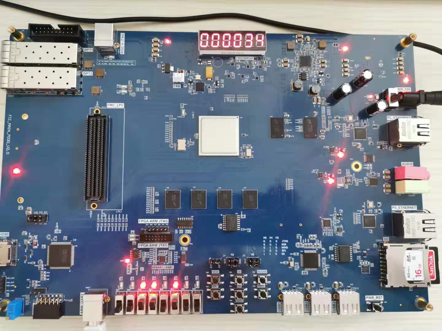
Figure 11.3 IIC transmission experimental phenomenon