FPGA
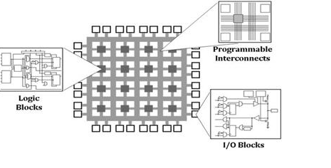
Field Programmable Gate Arrays (FPGAs) are semiconductor devices that are based around a matrix of configurable logic blocks (CLBs) connected via programmable interconnects. FPGAs can be reprogrammed to desired application or functionality requirements after manufacturing.
or simply perform basic logic gates, such as AND and OR. Most FPGAs also contain memory blocks (for more on these topics, see the section “The building blocks of an FPGA”).
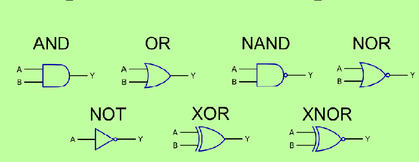
A logic gate is an elementary building block of a digital circuit. Most logic gates have two inputs and one output. At any given moment, every terminal is in one of the two binary conditions low (0) or high (1), represented by different voltage levels. The logic state of a terminal can, and generally does, change often, as the circuit processes data. In most logic gates, the low state is approximately zero volts (0 V), while the high state is approximately five volts positive (+5 V).
There are seven basic logic gates: AND, OR, XOR, NOT, NAND, NOR, and XNOR.
In FPGAs, there is no processor to run the software and we are the one designing the circuit. We can configure an FPGA as simple as an AND gate or a complex as the multi-core processor.To create a design we write Hardware Description Language (HDL), which is of two types – Verilog and VHDL. Then the HDL is synthesized into a bit file using a BITGEN to configure the FPGA.
FPGA Architecture
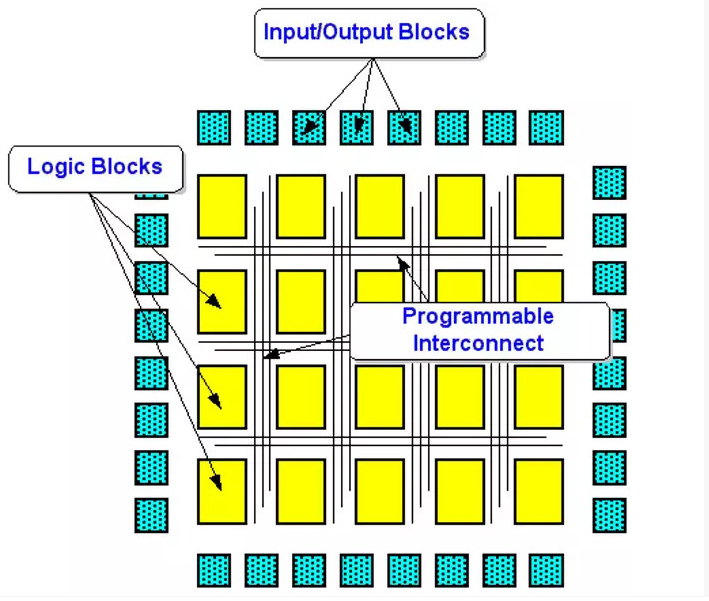
The FPGA Architecture consists of three major components
-
- Configurable logic blocks, which implement logic functions – The block contains RAM for creating arbitrary combinatorial logic functions, also known as lookup tables (LUTs). It also contains flip-flops for clocked storage elements, along with multiplexers in order to route the logic within the block and to and from external resources.
- Programmable Routing (interconnects), which implements functions – is used to bring signals onto the chip and send them back off again. It consists of an input buffer and an output buffer with three-state and open collector output controls.
- configurable I/O blocks, which are used to make off-chip connections – There are long lines that can be used to connect critical CLBs that are physically far from each other on the chip without inducing much delay. Theses long lines can also be used as buses within the chip.There are also short lines that are used to connect individual CLBs that are located physically close to each other. Transistors are used to turn on or off connections between different lines. There are also several programmable switch matrices in the FPGA to connect these long and short lines together in specific, flexible combinations.
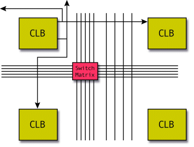
Three-state buffers are used to connect many CLBs to a long line, creating a bus. Special long lines, called global clock lines, are specially designed for low impedance and thus fast propagation times. These are connected to the clock buffers and to each clocked element in each CLB. This is how the clocks are distributed throughout the FPGA, ensuring minimal skew between clock signals arriving at different flip-flops within the chip.
In an ASIC, the majority of the delay comes from the logic in the design, because logic is connected with metal lines that exhibit little delay. In an FGPA, however, most of the delay in the chip comes from the interconnect, because the interconnect – like the logic – is fixed on the chip. In order to connect one CLB to another CLB in a different part of the chip often requires a connection through many transistors and switch matrices, each of which introduces extra delay.
Also, there will be clock circuitry for driving the clock signals to each logic block. Additional logic resources such as ALUs, memory, and decoders may also be available.
The role of the control unit in the FPGA is done by the programmable logic connection between each control unit and the unit in the figure. Through FPGA programming, the developer can change the operation logic between each unit of the FPGA and the unit. Connected so that it achieves the same effect as a normal running program. It differs from the CPU in that it cannot handle instructions that have not been programmed.
Once the programming method is determined, the FPGA can only process specific data inputs based on the processing logic and method being programmed. However, this architecture is replaced by almost all computing units inside the FPGA, so the actual computing power of the FPGA will be much stronger than it looks, especially when running tasks with simple but repetitive tasks. Several logical units, even one, can output the result of this operation independently. Since the two steps of fetching and decoding of the CPU are omitted, the efficiency of the FPGA repeatedly running the same code is greatly improved.
There is a metaphor that is very appropriate. The CPU is like a highly respected old professor in the university. The integral differential will be counted, but after all, it has only one person. When the calculation task is too heavy, it will be cumbersome, and the FPGA is like this. The structure is like a queue of all the primary school students in the primary school. Everyone will only count as simple addition, subtraction, multiplication and division, but some large but uncomplicated computing tasks will be given to them faster.
Specifically, in performance, it is obvious that a general CPU can only process 4 to 8 instructions at the same time, not too bad. As long as the FPGA is properly optimized, it can process 256 or more instructions at the same time. In fact, the design idea of the GPU is similar to that of the FPGA, and it is a device that appears to deal with a large number of simple and repeated operations. However, the performance of the GPU is strong and the energy consumption is also high. Because the FPGA is programmed and optimized directly at the hardware level, the energy consumption will be much lower.
How Do You Program an FPGA?
FPGA development does not require thorough knowledge of CLB functionality or painstaking arrangement of internal interconnects,FPGAs are always supported by development software that carries out the complicated process of converting a hardware design into the programming bits that determine the behavior of interconnects and CLBs. We use Hardware Description Languages to program in FPGA, and the two most common are VHDL and Verilog. Despite the apparent similarity between HDL code and code written in a high-level software programming language, the two are fundamentally different. Software code specifies a sequence of operations, whereas HDL code is more like a schematic that uses text to introduce components and create interconnections.
We include the PLL1 generated in Experiment 1 Verilog HDL code is as follows:
module SW_LED(

input inclk,
input [7:0] sw,
output reg [7:0] led
);

wire sys_clk;
wire pll_locked;
reg sys_rst;

always@(posedge sys_clk)
sys_rst<=!pll_locked;

always @(posedge inclk)
if(sys_rst)
led<=8’hff;
else
led<=~sw;

PLL1 PLL1_INST

(
.areset (1’b0),
.inclk0 (inclk),
.c0 (sys_clk),
.locked (pll_locked)
);

endmodule
Basic FPGA process technology types
- SRAM – based on static memory technology. In-system programmable and re-programmable. Requires external boot devices. CMOS. Currently in use.[when?] Notably, flash memory or EEPROM devices may often load contents into internal SRAM that controls routing and logic.
- Fuse – One-time programmable. Bipolar. Obsolete.
- Antifuse – One-time programmable. CMOS.
- PROM – Programmable Read-Only Memory technology. One-time programmable because of plastic packaging. Obsolete.
- EPROM – Erasable Programmable Read-Only Memory technology. One-time programmable but with window, can be erased with ultraviolet (UV) light. CMOS. Obsolete.
- EEPROM – Electrically Erasable Programmable Read-Only Memory technology. Can be erased, even in plastic packages. Some but not all EEPROM devices can be in-system programmed. CMOS.
- Flash – Flash-erase EPROM technology. Can be erased, even in plastic packages. Some but not all flash devices can be in-system programmed. Usually, a flash cell is smaller than an equivalent EEPROM cell and is therefore less expensive to manufacture. CMOS.
FPGA Applications
Due to their programmable nature, FPGAs are an ideal fit for many different markets. As the industry leader, Xilinx provides comprehensive solutions consisting of FPGA devices, advanced software, and configurable, ready-to-use IP cores for markets and applications such as:
-
- Aerospace & Defense – Radiation-tolerant FPGAs along with intellectual property for image processing, waveform generation, and partial reconfiguration for SDRs.
- ASIC Prototyping – ASIC prototyping with FPGAs enables fast and accurate SoC system modeling and verification of embedded software
- Audio – Xilinx FPGAs and targeted design platforms enable higher degrees of flexibility, faster time-to-market, and lower overall non-recurring engineering costs (NRE) for a wide range of audio, communications, and multimedia applications.
- Automotive – Automotive silicon and IP solutions for gateway and driver assistance systems, comfort, convenience, and in-vehicle infotainment. – Learn how Xilinx FPGA’s enable Automotive Systems
- Broadcast & Pro AV – Adapt to changing requirements faster and lengthen product life cycles with Broadcast Targeted Design Platforms and solutions for high-end professional broadcast systems.
- Consumer Electronics – Cost-effective solutions enabling next generation, full-featured consumer applications, such as converged handsets, digital flat panel displays, information appliances, home networking, and residential set top boxes.
- Data Center – Designed for high-bandwidth, low-latency servers, networking, and storage applications to bring higher value into cloud deployments.
- High Performance Computing and Data Storage – Solutions for Network Attached Storage (NAS), Storage Area Network (SAN), servers, and storage appliances.
- Industrial – Xilinx FPGAs and targeted design platforms for Industrial, Scientific and Medical (ISM) enable higher degrees of flexibility, faster time-to-market, and lower overall non-recurring engineering costs (NRE) for a wide range of applications such as industrial imaging and surveillance, industrial automation, and medical imaging equipment.
- Medical – For diagnostic, monitoring, and therapy applications, the Virtex FPGA and Spartan® FPGA families can be used to meet a range of processing, display, and I/O interface requirements.
- Security – Xilinx offers solutions that meet the evolving needs of security applications, from access control to surveillance and safety systems.
- Video & Image Processing – Xilinx FPGAs and targeted design platforms enable higher degrees of flexibility, faster time-to-market, and lower overall non-recurring engineering costs (NRE) for a wide range of video and imaging applications.
- Wired Communications – End-to-end solutions for the Reprogrammable Networking Linecard Packet Processing, Framer/MAC, serial backplanes, and more
- Wireless Communications – RF, base band, connectivity, transport and networking solutions for wireless equipment, addressing standards such as WCDMA, HSDPA, WiMAX and others.
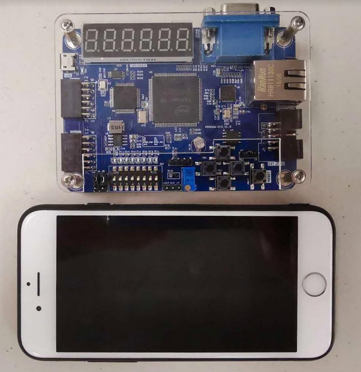
FPGA Board for Beginner