FPGA Board
A development board is actually a printed circuit board (PCB) with some circuitry and hardware on-board to facilitate experimentation with a dedicated chip. These boards can save you from a lot of repetitive tasks. Imagine, you want to work on an FPGA-based project, but to be able to use an FPGA chip you need to solder this chip on the PCB as you cannot breadboard it. Also, you will have to set up a bunch of circuitry and hardware interfaces every time you want to work with that chip for different projects.
FPGAs contain an array of programmable logic blocks, and a hierarchy of reconfigurable interconnects that allow the blocks to be “wired together”, like many logic gates that can be inter-wired in different configurations. Logic blockscan be configured to perform complex combinational functions, or merely simple logic gates like AND and XOR. In most FPGAs, logic blocks also include memory elements, which may be simple flip-flops or more complete blocks of memory. Many FPGAs can be reprogrammed to implement different logic functions, allowing flexible reconfigurable computing as performed in computer software.
FPGAs are quite a complex device and, to build a project on a development board, it is important that you know how the interfaces and other hardware is wired on the board. Most manufacturers have proper legends on the board to indicate the interfaces but wiring sometimes can be difficult to trace. So check that the manufacturer provides complete schematic diagram, a reference manual, getting started guide, reference designs and sample codes.
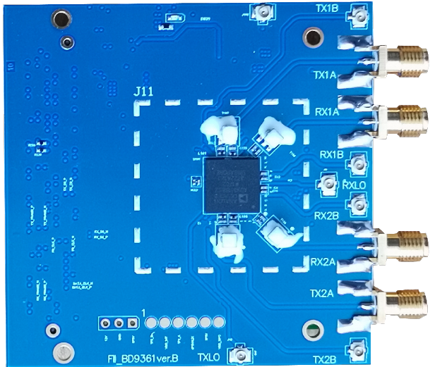
The AD9361 RF Agile Transceiver™ is a FPGA development board that is designed from the ground up to be easy to use Ad9361. The AD9361 is a high performance, highly integrated radio frequency (RF) Agile Transceiver™ designed for use in 3G and 4G base station applications. Its programmability and wideband capability make it ideal for a broad range of transceiver applications.
The entire goal of the AD9361 FPGA Development Board is to make getting started with FPGA and digital design as easy as possible. To go along with the dev board there is a set of tutorials to help you get started and expand your knowledge of digital design.
Description
FII-BD9361 – Completely Compatible with AD-FMCOMMS3-EBZ Board $379
The AD-FMCOMMS3-EBZ provides software developers and system architect who want a single platform to operate over a wider tuning range than the AD-FMCOMMS2-EBZ. RF performance expectations of this board must be tempered with the very wide band front end. It does meet the datasheet specifications at 2.4 GHz, but does not over the entire RF tuning range that the board supports. Typical performance data for the entire range (70 MHz – 6 GHz) which is supported by the platform is published within the board documentation. This board is primarily intended for system investigation and bringing up various waveforms from a software team before custom hardware is complete. The objective being for designers to see waveforms, but not being concerned about the last 1dB or 1% EVM of performance.
Features and Benefits
-
Software tunable across wide frequency range : TX :47 MHz to 6 GHz RX:70 MHz to 6 GHz
-
Software tunable bandwidth: 200 kHz to 56 MHz.
-
Software tunable TX Power and RX Dynamic Range:TX>80dB RX>70dB
-
Powered up from single standard FMC connector
-
Supports MIMO radio,2 ways TX and 2 ways RX(Max 4T4R by RF Switches configuration)
-
Supports FII-7030 and other standard FMC Connector Platform software radio application