Description
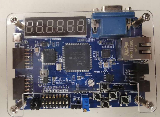
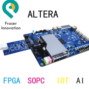
The advantage of FPGA beginner study board:
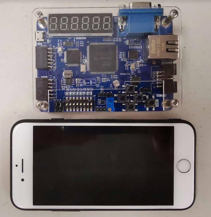
- Beginner FPGA study board, cheaper but fully functional. cellphone sized. ( < 100 USD )
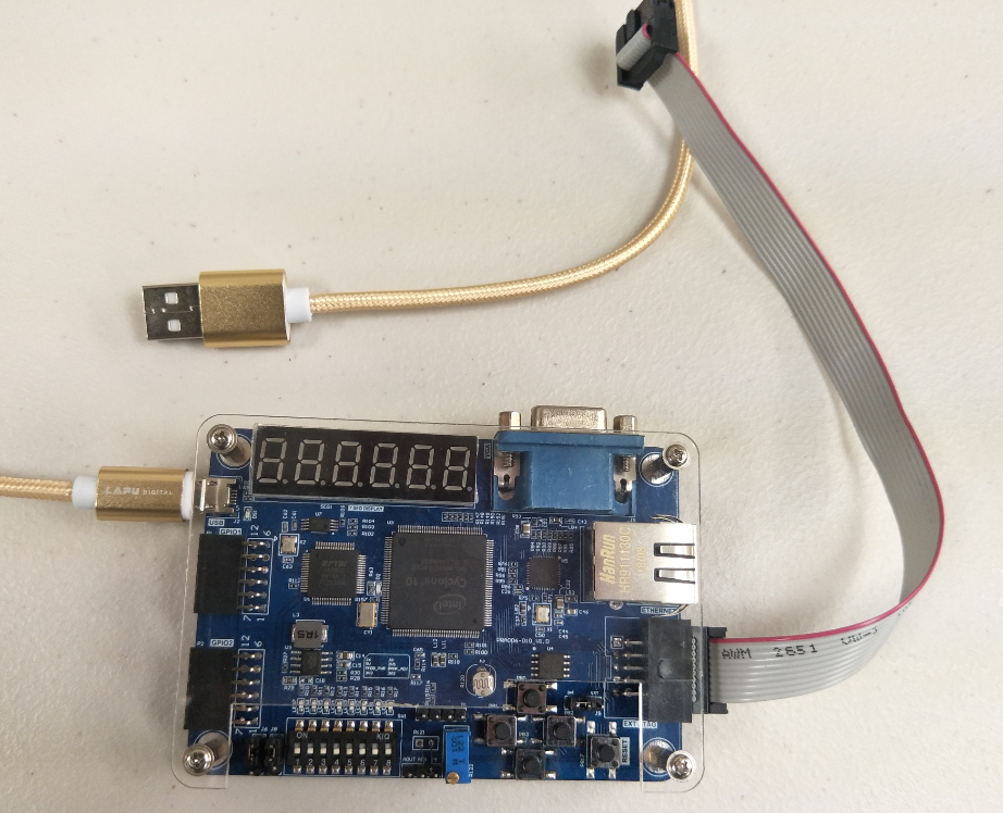
- power supply and download at the same time, no extra power supply and no extra data transfer line needed
- Small volume and light and can be put into your pocket. size: 10cm X 7 cm.
- Unique function: can be a study board as well a multifunctional JTAG downloader.
- We use newest version Intel FPGA within two years and you can always keep in the front of FPGA industry.
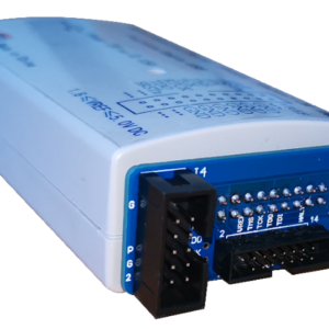
FII-PRA006 is both a FPGA development board and a JTAG down-loader. As a JTAG down-loader, It support:
- Intel(Altera) FPGA:Support Quartus II5.0 and all the version afterwords;
- Xilinx FPGA:Support ISE9.0 and all version afterwords or All Vivado versions;
- Compatible with ARM Cortext:Support OpenOCD
- RISC-V CPU:Support FreeDomStudio,including GCC、OpenOCD、and GDB Debugging
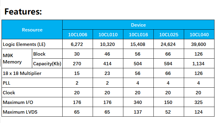
FPGA Study Board HeardWare Features
The Biggest Hardware Benefits:
-
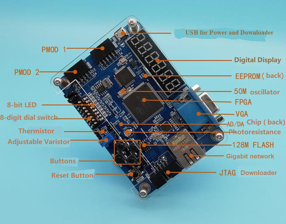
- USB port for power supply, downloader, communications ;
- One 50M Oscillator. A stable clock for development board;
- 6-digit common anode digital tube,display the data by dynamic scan;
- 1 VGA port to display picture and video;
- 1 I2C port EEPROM chip,Model: AT24C02;
- 1 adaptive 10M, 100M/1000M Ethernet port;
- 5 buttons,4 for programmable buttons , and one button for resetting;
- 1 Photoresistance. It can be used for simulating light control;
- 1 thermistor. It can be used for collecting temperature or simulating alarm function
- An adjustable resistor can simulate voltage changes, etc.
- 1 PCF8591 AD/DA Conversion chip;
- 8-digit dial switch;
- 8-bit LED light-emitting diode;
- One 128Mbit Flash Chip;
- 2 GPIO external port for communication extension port ;
- One JTAGPort , and make PRA006/010 a functional JTAG down-loader, can be used as a JTAG downloader for Intel,Xilinx and other FPGA downloadable program;
FPGA Type: 10CL006
Altera FPGA Study Board Hardware Resources:
- 6 seven_seg_r
- VGA Video Interface × 1
- 1G Ethernet Interface × 1
- I2C EEPROM × 1
- DIP Switch × 8
- Controllable LED light × 8
- Photoresistance × 1
- Thermistor × 1
- Adjustable Varistor × 1
- Buttons × 4
- GPIO Interface × 2
- Micro usb Interface(Power Supply and downlaod ) × 1
- SPI Communication Interface × 1
- AD/DA Conversion chip × 1
- JTAG Download Interface × 1
- FLASH 32Mbit × 1
It can also be used with other FPGA development Boards:
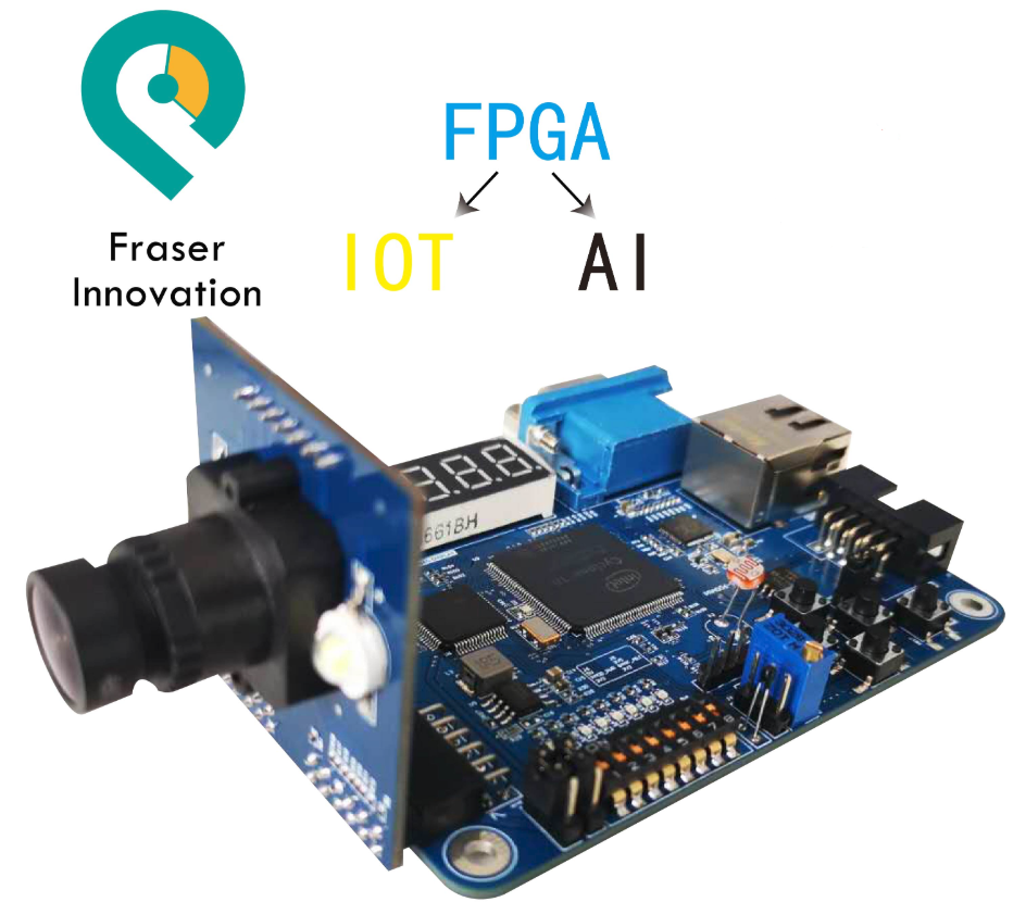
FPGA Board for Beginners embeded with JTag
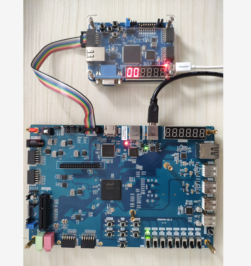
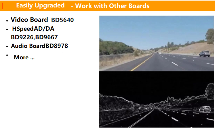
We will send you following documents when you have bought our PRA006 or PRA010 pocket board for beginners:
We will send you following documents after you have bought our products:
The experimental manual of FII-PRA006 and FII-PRA010 pocket Board for beginners
The Hardware Configuration of FII-PRA006 and FII-PRA010 Board for beginners
The Schematic Diagram of FII-PRA006 and FII-PRA010 FPGA Board for beginners

JTAG Configuration Description – FII-PRA006 – Cyclone-10 FPGA Development Board with Jtag Embeded
The latest DLL versions for Altera Quartus II or Intel Quartus Prime are 1.8b (Provided in the folder), for Quartus in Linux, get version 1.7b.
To install the driver for Quartus II, do the following:
- Connect the MBFTDI programmer with a USB cable to a Windows computer.
- Make sure the device is detected and the FTDI drivers are already installed. To do this, look in the Device Manager Windows, in the COM and LPT ports section, two COM ports should appear. If instead you find two yellow question marks, then you need to install the FTDI drivers. The related files CDM20814_WHQL_Certified are attached as well.
- Determine the type of jtagserver that runs on your computer. This service is part of Altera Quartus II, but you need to understand exactly if you have a Win32 or x64 version of jtagserver. If a 32-bit Windows XP or Windows 7 OS is installed, then there is nothing to think about – of course, and jtagserver will be 32-bit. But if the OS is 64-bit, then immediately it is difficult to say for sure. The most reliable way to determine the type of jtagserver is to view its properties in the “Computer Management – Services” dialog:
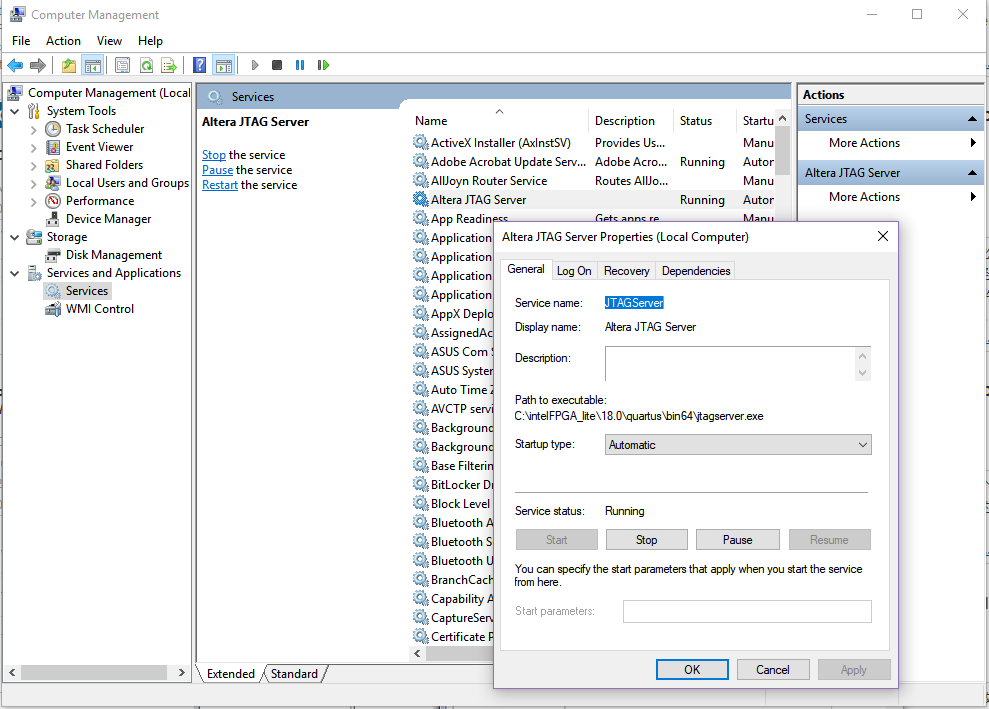
Here you can see in this picture that the used jtagserver is in the bin64 folder, which means that the 64-bit version of the server is used. Remember the path to it.
- Use either 64-bit or 32-bit driver. In this archive there are two files, respectively for win32 and win_x64. The driver is called jtag_hw_mbftdi_blaster32.dll or jtag_hw_mbftdi_blaster64.dll. If you have a 32-bit jtagserver, then take the first file. If you have it 64-bit, then take the second DLL. Rewrite jtag_hw_mbftdi_blasterXX.dll the location where lies jtagserver (see picture above). Usually the folder name looks something like this: C:\intelFPGA_lite\18.0\quartus\bin or C:\intelFPGA_lite\18.0\quartus\bin64 (The actual path may differ depending on the quartus version).
- Where there is a jtagserver, rewrite another DLL from the FTDI driver set (see step 2). File name: ftd2xx.dll or ftd2xx64.dll respectively for win32 or x64 (this step is optional).
Online Shopping Website:
https://fpgamarketing.com/FPGA-Study-Board-Verilog-for-beginner-Cyclone-10-FII-PRA006-FII-PRA006.htm
We will send you experimental manuals when you have bought our pocket study board. PRA006 or PRA010
The Benefits of FPGA
Flexibility
- FPGA functionality can change upon every power-up of the device. So, when a design engineer wants to make a change, they can simply download a new configuration file into the device and try out the change.
- Often, changes can be made to the FPGA without making costly PC board changes.
- ASSPs and ASICs have fixed hardware functionality that can’t be changed without great cost and time.
Acceleration
- FPGAs are sold “off the shelf” vs. ASICs (which require manufacturing cycles taking many months).
- Because of FPGA flexibility, OEMs can ship systems as soon as the design is working and tested.
- FPGAs provide off-load and acceleration functions to CPUs, effectively speeding up the entire system performance.
Integration
Today’s FPGAs include on-die processors, transceiver I/O’s at 28 Gbps (or faster), RAM blocks, DSP engines, and more. More functions within the FPGA mean fewer devices on the circuit board, increasing reliability by reducing the number of device failures.
Total Cost of Ownership (TCO)
- While ASICs may cost less per unit than an equivalent FPGA, building them requires a non-recurring expense (NRE), expensive software tools, specialized design teams, and long manufacturing cycles.
- Intel FPGAs support long lifecycles (15-years or more), avoiding the cost of redesigning and requalifying OEM production equipment if one of the electronic devices on-board goes end of life (EOL).
- FPGAs reduce risk, allowing prototype systems to ship to customers for field trials, while still providing the ability to make changes quickly before ramping to volume production.
The concept behind an FPGA’s programmability is a basic building block containing various logic types that are connected and interconnected to perform any logic function. “Basic building block” is a generic term that I’m using, but you may hear terms like “logic cells,” “combinational logic blocks” (CLBs), or “logic array blocks” (LABs); it depends on the manufacturer. The basic building block contains logic resources and is the starting point that the FPGA uses to constructs the design.
We will send you above documents after you have bought our PRA006 pocket study board.
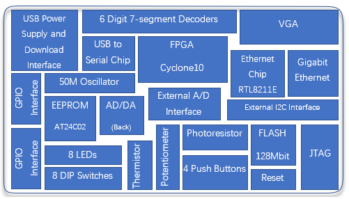
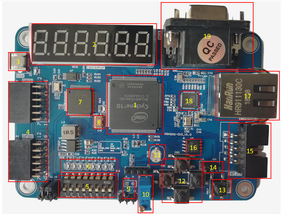
What is the main components of the FRA006 FPGA beginner board ?
-
- 10CL006YE144C8G or 10CL006YE144C8G
- 6-digit common anode seven-segment display
- USB power supply and download interface
- External expansion interface GPIO
- 8 DIP switches
- 8 LEDs
- USB to serial port chip (FT2232)(Intefrated JTAG download function)
- 50 MHz oscillator
- Thermistor (NTC-MF52)
- Potentiometer
- Photoresistor
- 4 buttons (up, down, right, down)
- Reset button (Reset)
- JTAG downloader function conversion interface
- JTAG download interface (Used only when the board is used as a downloader)
- Flash (N25Q128A, 128M bit/16M bytes)
- Ethernet interface
- Ethernet PHY chip (RTL8211E-VB)
- VGA interface
- Back of the board U8: AD/DA conversion chip (PCF8591)
- Back of the board U13: EEPROM (AT24C02N)
Extension Experiments
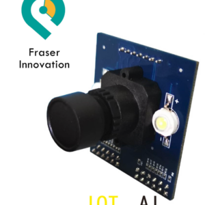
Video Camera
- Pictures and Videos Collection
- Edge check and human-face location Positioning
- Picture and video Zip and UnZip
Voice and Speech
- voice and speech collection
- Speech Recognition
- High Speed Analog signal acquisition
Risc-V
- Low level CPU programing
- Run C language
- C language debugging onboard device
If you have any questions, you can contact us or post in the FII-PRA006 and FII-PRA010 product forums. If you can not register to post, please let us know and I will create a forum username for you.
FPGA for beginner Tutorial
- FPGA Board for Beginner
- FPGA Board Beginner Tutorial – FII-PRA006 Experiment 1 LED_shifting
- FPGA for Beginner Tutorial – Experiment 2 Switch and Use SignalTap II – FII-PRA006
- FPGA for Beginner Tutorial – Experiment 3 – BCD_counter – FII-PRA006
- FPGA Tutorial – Block/ Schematic Test – FPGA Board for Beginner – Experiment 4
- FPGA tutorial – Block_debouncing – FBGA Board for for beginner – Experiment 5
- FPGA Tutorial – Use Multiplier and ModelSim – FPGA Board for Beginner – Experiment 6
- FPGA Tutorial – Hexadecimal Numbers to BCD Code Conversion and Application – FPGA Board for Beginner – Experiment 7
- FPGA Tutorial – Use of ROM (Read-only Memory) – FPGA Board for Beginner – Experiment 8
- FPGA Tutorial – Use Dual-port RAM to Read and Write Frame Data – FPGA Board for Beginner – Experiment 9
- FPGA Tutorial – Asynchronous Serial Port Design and Experiment – FPGA for Beginner – Experiment 10
- FPGA Beginner Tutorial – IIC Protocol Transmission – FPGA Board for Beginner – Experiment 11
- FPGA Beginner Tutorial – AD, DA Experiment – FPGA Board for Beginner – Experiment 12
- FPGA Beginner Tutorial – VGA Experiment – FPGA Board for Beginner – Experiment 13
- FPGA Beginner Tutorial – Ethernet Experiment – FPGA Board for Beginner – Experiment 14
- FPGA Board for beginner – FII-PRA006/010 Hardware Reference Guide


Reviews
There are no reviews yet.