FPGA Beginner Tutorial – AD, DA Experiment – FPGA Board for Beginner – Experiment 12
Experiment 12 AD, DA Experiment
12.1 Experiment Objective
Since in the real world, all naturally occurring signals are analog signals, and all that are read and processed in actual engineering are digital signals. There is a process of mutual conversion between natural and industrial signals (digital-to-analog conversion: DAC, analog-to-digital conversion: ADC). The purpose of this experiment is twofold:
- Learning the theory of AD conversion
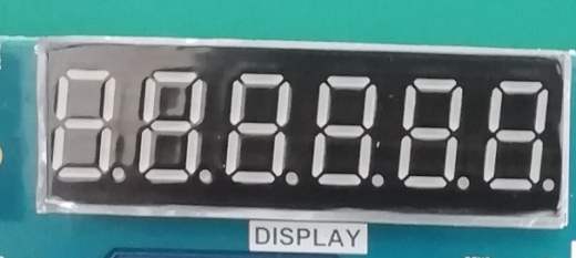
- Read the value of AD acquisition from PCF8591, and convert the value obtained into actual value, display it with segment decoders
12.2 Experiment Requirement
-
- Perform analog-to-digital conversion using the ADC port of the chip and display the collected voltage value through the segment decoders.
- Board downloading verification for comparison
- Introduction to PCF8591: The PCF8591 uses the IIC bus protocol to communicate with the controller (FPGA). Please refer to the previous experiment for the contents of the IIC bus protocol. The first four bits of the device address are 1001, and the last three bits are determined by the actual circuit connection (here the circuit is grounded, so the device address is 7’b1001000). The LSB is the read/write control signal. After sending the device address information and the read/write control word are done, the control word information is sent. The specific control word information is shown in Figure 12. 1.
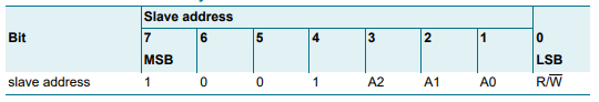
Fig 12. 1 PCF8591 address byte
Here, the experiment uses the DIP switch (SW1, SW0) input channel as the AD acquisition input channel. Configure the control information as (8’h40). For more details, refer to the datasheet of PCF8591.
| SW1,SW0 | Channel Selection | Collection Object |
| 00 | 0 | Photosensitive Resistor Voltage Value |
| 01 | 1 | Thermistor Voltage Value |
| 10 | 2 | Adjustable Voltage Value |
12.3 Experiment
- Program design and review the top-down design method used before.
- The top-level entity is divided into three parts: the segment decoder driver part, the AD sampling part of the PCF and the IIC serial port driver part.
- Refer to the project file adda_test for the program part.
12.4 Downloading to the Board
| Signal Name | Port Description | Network Label | FPGA Pin |
| clk | System clock 50MHz | C10_50MCLK | 91 |
| rst | Reset, default value is low | KEY3 | 11 |
| sm_db[0] | Segment decoder seg a | SEG_PA | 132 |
| sm_db [1] | Segment decoder seg b | SEG_PB | 137 |
| sm_db [2] | Segment decoder seg c | SEG_PC | 133 |
| sm_db [3] | Segment decoder seg d | SEG_PD | 125 |
| sm_db [4] | Segment decoder seg e | SEG_PE | 126 |
| sm_db [5] | Segment decoder seg f | SEG_PF | 138 |
| sm_db [6] | Segment decoder seg g | SEG_PG | 135 |
| sm_db [7] | Segment decoder seg h | SEG_DP | 128 |
| data[0] | DIP switch input | SW0 | 80 |
| data[1] | DIP switch input | SW1 | 83 |
| data[2] | DIP switch input | SW2 | 86 |
| data[3] | DIP switch input | SW3 | 87 |
| data[4] | DIP switch input | SW4 | 74 |
| data[5] | DIP switch input | SW5 | 75 |
| data[6] | DIP switch input | SW6 | 76 |
| data[7] | DIP switch input | SW7 | 77 |
| scl | PCF8591 clock line | ADDA_I2C_SCL | 53 |
| sda | PCF8591 data line | ADDA_I2C_SDA | 52 |
| sel[0] | Segment decoder position selection | SEG_3V3_D0 | 124 |
| sel[1] | Segment decoder position selection | SEG_3V3_D1 | 127 |
| sel[2] | Segment decoder position selection | SEG_3V3_D2 | 129 |
| sel[3] | Segment decoder position selection | SEG_3V3_D3 | 141 |
| sel[4] | Segment decoder position selection | SEG_3V3_D4 | 142 |
| sel[5] | Segment decoder position selection | SEG_3V3_D5 | 136 |
Note: The six segment decoders are reversed in order due to actual observations.
Visited 1 times, 1 visit(s) today