FPGA Beginner Tutorial – IIC Protocol Transmission – FPGA Board for Beginner – Experiment 11
Experiment 11 IIC Protocol Transmission
11.1 Experiment Objective
There is an IIC interface EEPROM chip 24LC02 in the test plate, capacity sized 2 kbit (256 bite). Since the data is not lost after the EEPROM is powered down, users can store some hardware setup data or user information.
Learning the basic principles of the different IIC bus, mastering the IIC communication protocol
Master the method of reading and writing EEPROM
Joint debugging using logic analyzer
11.2 Experiment Requirement
-
-
-
- Correctly write a number to any address in the EEPROM (this experiment writes to the register of 8’h03 address) through the FPGA (here changes the written 8-bit data value by (SW7~SW0)). After writing in successfully, read the data as well. The read data is displayed directly on the segment decoders.
- Download the program into the FPGA and press the left push button PB1 to execute the data write EEPROM operation. Press the right push button PB2 to read the data that was just written.
- Determine whether the value read is correct or not by reading the value displayed on the segment decoders. If the segment decoders display the same value as written value, the experiment is successful.
- Analyze the correctness of the internal data with SignalTap II and verify it with the display of the segment decoders.
-
-
11.3 Introduction to the IIC Agreement
11.3.1 The Overall Timing Protocol of IIC Is as Follows
Bus idle state: SDA, SCL are high
Start of IIC protocol: SCL stays high, SDA jumps from high level to low level, generating a start signal
IIC read and write data phase: including serial input and output of data and response model issued by data receiver
IIC transmission end bit: SCL is high level, SDA jumps from low level to high level, and generates an end flag. See Fig 11. 1
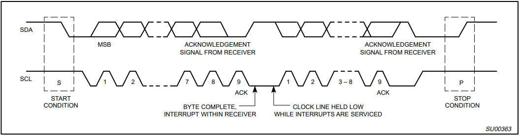
Figure 11. 1 Timing protocol of IIC
11.3.2 IIC Device Address
Each IIC device has a device address. When some device addresses are shipped from the factory, they are fixed by the manufacturer (the specific data can be found in the manufacturer’s data sheet). Some of their higher bits are determined, and the lower bits can be configured by the user according to the requirement. The higher four-bit address of the EEPROM chip 24LC02 used by the develop board has been fixed to 1010 by the component manufacturer. The lower three bits are linked in the develop board as shown below, so the device address is 1010000. See Fig 11. 2
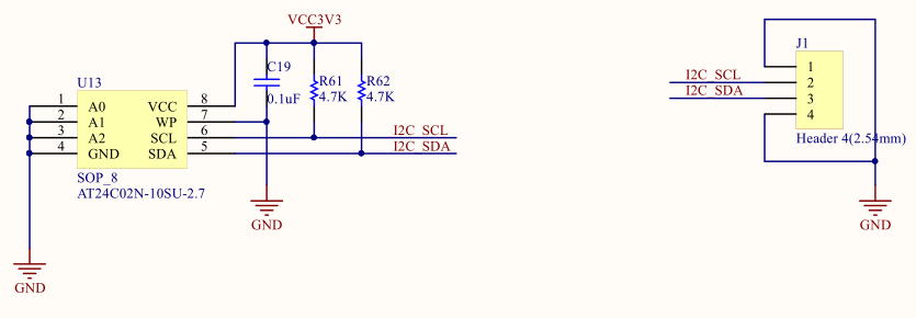
Fig 11. 2 Device schematics of IIC
11.4 The Key Code of Experiment, IIC_COM.v
module iic_com(
clk,rst,
data,
sw1,sw2,
scl,sda,
iic_done,
dis_data
);
input clk; // 50MHz
input rst;
input sw1,sw2;
inout scl;
inout sda;
output[7:0] dis_data;
input [7:0] data ;
output reg iic_done =0 ;
reg [7:0] data_tep;
reg scl_link ;
reg [19:0] cnt_5ms ;
reg sw1_r,sw2_r;
reg[19:0] cnt_20ms;
always @ (posedge clk or posedge rst_n)
if(rst) cnt_20ms <= 20’d0;
else cnt_20ms <= cnt_20ms+1’b1;
always @ (posedge clk or posedge rst)
if(rst) begin
sw1_r <= 1’b0;
sw2_r <= 1’b0;
end
else if(cnt_20ms == 20’hfffff) begin
sw1_r <= sw1;
sw2_r <= sw2;
end
//———————————————
reg[2:0] cnt;
reg[8:0] cnt_delay;
reg scl_r;
always @ (posedge clk or posedge rst)
if(rst) cnt_delay <= 9’d0;
else if(cnt_delay == 9’d499) cnt_delay <= 9’d0;
else cnt_delay <= cnt_delay+1’b1;
always @ (posedge clk or negedge rst) begin
if(rst) cnt <= 3’d5;
else begin
case (cnt_delay)
9’d124: cnt <= 3’d1; //cnt=1:scl
9’d249: cnt <= 3’d2; //cnt=2:scl
9’d374: cnt <= 3’d3; //cnt=3:scl
9’d499: cnt <= 3’d0; //cnt=0:scl
default: cnt<=3’d5;
endcase
end
end
`define SCL_POS (cnt==3’d0) //cnt=0:scl
`define SCL_HIG (cnt==3’d1) //cnt=1:scl
`define SCL_NEG (cnt==3’d2) //cnt=2:scl
`define SCL_LOW (cnt==3’d3) //cnt=3:scl
always @ (posedge clk or posedge rst)
if(rst_n) data_tep <= 8’h00;
else data_tep<= data ; //
always @ (posedge clk or negedge rst)
if(rst) scl_r <= 1’b0;
else if(cnt==3’d0) scl_r <= 1’b1; //scl
else if(cnt==3’d2) scl_r <= 1’b0; //scl
assign scl = scl_link?scl_r: 1’bz ;
//———————————————
`define DEVICE_READ 8’b1010_0001
`define DEVICE_WRITE 8’b1010_0000
`define WRITE_DATA 8’b1000_0001
`define BYTE_ADDR 8’b0000_0011
reg[7:0] db_r;
reg[7:0] read_data;
//———————————————
parameter IDLE = 4’d0;
parameter START1 = 4’d1;
parameter ADD1 = 4’d2;
parameter ACK1 = 4’d3;
parameter ADD2 = 4’d4;
parameter ACK2 = 4’d5;
parameter START2 = 4’d6;
parameter ADD3 = 4’d7;
parameter ACK3 = 4’d8;
parameter DATA = 4’d9;
parameter ACK4 = 4’d10;
parameter STOP1 = 4’d11;
parameter STOP2 = 4’d12;
reg[3:0] cstate;
reg sda_r;
reg sda_link;
reg[3:0] num;
always @ (posedge clk or posedge rst) begin
if(rst) begin
cstate <= IDLE;
sda_r <= 1’b1;
scl_link <= 1’b1;
sda_link <= 1’b1;
num <= 4’d0;
read_data <= 8’b0000_0000;
cnt_5ms <=20’h00000 ;
iic_done<=1’b0 ;
end
else
case (cstate)
IDLE: begin
sda_link <= 1’b1;
scl_link <= 1’b1;
iic_done<=1’b0 ;
if(sw1_r || sw2_r) begin
db_r <= `DEVICE_WRITE;
cstate <= START1;
end
else cstate <= IDLE;
end
START1: begin
if(`SCL_HIG) begin
sda_link <= 1’b1;
sda_r <= 1’b0;
cstate <= ADD1;
num <= 4’d0;
end
else cstate <= START1;
end
ADD1: begin
if(`SCL_LOW) begin
if(num == 4’d8) begin
num <= 4’d0;
sda_r <= 1’b1;
sda_link <= 1’b0;
cstate <= ACK1;
end
else begin
cstate <= ADD1;
num <= num+1’b1;
case (num)
4’d0: sda_r <= db_r[7];
4’d1: sda_r <= db_r[6];
4’d2: sda_r <= db_r[5];
4’d3: sda_r <= db_r[4];
4’d4: sda_r <= db_r[3];
4’d5: sda_r <= db_r[2];
4’d6: sda_r <= db_r[1];
4’d7: sda_r <= db_r[0];
default: ;
endcase
// sda_r <= db_r[4’d7-num];
end
end
// else if(`SCL_POS) db_r <= {db_r[6:0],1’b0};
else cstate <= ADD1;
end
ACK1: begin
if(/*!sda*/`SCL_NEG) begin
cstate <= ADD2;
db_r <= `BYTE_ADDR;
end
else cstate <= ACK1;
end
ADD2: begin
if(`SCL_LOW) begin
if(num==4’d8) begin
num <= 4’d0;
sda_r <= 1’b1;
sda_link <= 1’b0;
cstate <= ACK2;
end
else begin
sda_link <= 1’b1;
num <= num+1’b1;
case (num)
4’d0: sda_r <= db_r[7];
4’d1: sda_r <= db_r[6];
4’d2: sda_r <= db_r[5];
4’d3: sda_r <= db_r[4];
4’d4: sda_r <= db_r[3];
4’d5: sda_r <= db_r[2];
4’d6: sda_r <= db_r[1];
4’d7: sda_r <= db_r[0];
default: ;
endcase
// sda_r <= db_r[4’d7-num];
cstate <= ADD2;
end
end
// else if(`SCL_POS) db_r <= {db_r[6:0],1’b0};
else cstate <= ADD2;
end
ACK2: begin
if(/*!sda*/`SCL_NEG) begin
if(sw1_r) begin
cstate <= DATA;
db_r <= data_tep;
end
else if(sw2_r) begin
db_r <= `DEVICE_READ;
cstate <= START2;
end
end
else cstate <= ACK2;
end
START2: begin
if(`SCL_LOW) begin
sda_link <= 1’b1;
sda_r <= 1’b1;
cstate <= START2;
end
else if(`SCL_HIG) begin
sda_r <= 1’b0;
cstate <= ADD3;
end
else cstate <= START2;
end
ADD3: begin
if(`SCL_LOW) begin
if(num==4’d8) begin
num <= 4’d0;
sda_r <= 1’b1;
sda_link <= 1’b0;
cstate <= ACK3;
end
else begin
num <= num+1’b1;
case (num)
4’d0: sda_r <= db_r[7];
4’d1: sda_r <= db_r[6];
4’d2: sda_r <= db_r[5];
4’d3: sda_r <= db_r[4];
4’d4: sda_r <= db_r[3];
4’d5: sda_r <= db_r[2];
4’d6: sda_r <= db_r[1];
4’d7: sda_r <= db_r[0];
default: ;
endcase
// sda_r <= db_r[4’d7-num];
cstate <= ADD3;
end
end
// else if(`SCL_POS) db_r <= {db_r[6:0],1’b0};
else cstate <= ADD3;
end
ACK3: begin
if(/*!sda*/`SCL_NEG) begin
cstate <= DATA;
sda_link <= 1’b0;
end
else cstate <= ACK3;
end
DATA: begin
if(sw2_r) begin
if(num<=4’d7) begin
cstate <= DATA;
if(`SCL_HIG) begin
num <= num+1’b1;
case (num)
4’d0: read_data[7] <= sda;
4’d1: read_data[6] <= sda;
4’d2: read_data[5] <= sda;
4’d3: read_data[4] <= sda;
4’d4: read_data[3] <= sda;
4’d5: read_data[2] <= sda;
4’d6: read_data[1] <= sda;
4’d7: read_data[0] <= sda;
default: ;
endcase
// read_data[4’d7-num] <= sda;
end
// else if(`SCL_NEG) read_data <= {read_data[6:0],read_data[7]};
end
else if((`SCL_LOW) && (num==4’d8)) begin
num <= 4’d0;
cstate <= ACK4;
end
else cstate <= DATA;
end
else if(sw1_r) begin
sda_link <= 1’b1;
if(num<=4’d7) begin
cstate <= DATA;
if(`SCL_LOW) begin
sda_link <= 1’b1;
num <= num+1’b1;
case (num)
4’d0: sda_r <= db_r[7];
4’d1: sda_r <= db_r[6];
4’d2: sda_r <= db_r[5];
4’d3: sda_r <= db_r[4];
4’d4: sda_r <= db_r[3];
4’d5: sda_r <= db_r[2];
4’d6: sda_r <= db_r[1];
4’d7: sda_r <= db_r[0];
default: ;
endcase
// sda_r <= db_r[4’d7-num];
end
// else if(`SCL_POS) db_r <= {db_r[6:0],1’b0};
end
else if((`SCL_LOW) && (num==4’d8)) begin
num <= 4’d0;
sda_r <= 1’b1;
sda_link <= 1’b0;
cstate <= ACK4;
end
else cstate <= DATA;
end
end
ACK4: begin
if(/*!sda*/`SCL_NEG) begin
// sda_r <= 1’b1;
cstate <= STOP1;
end
else cstate <= ACK4;
end
STOP1: begin
if(`SCL_LOW) begin
sda_link <= 1’b1;
sda_r <= 1’b0;
cstate <= STOP1;
end
else if(`SCL_HIG) begin
sda_r <= 1’b1;
cstate <= STOP2;
end
else cstate <= STOP1;
end
STOP2: begin
if(`SCL_NEG) begin sda_link <= 1’b0; scl_link <= 1’b0; end
else if(cnt_5ms==20’h3fffc) begin cstate <= IDLE; cnt_5ms<=20’h00000; iic_done<=1 ; end
else begin cstate <= STOP2 ; cnt_5ms<=cnt_5ms+1 ; end
end
default: cstate <= IDLE;
endcase
end
assign sda = sda_link ? sda_r:1’bz;
assign dis_data = read_data;
endmodule
11.5 Downloading to the Board
- Lock the pins
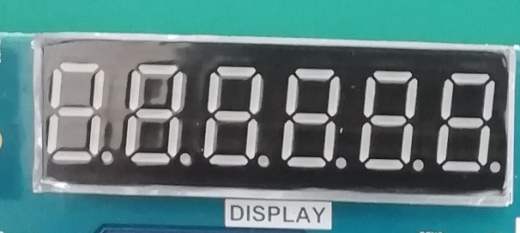
- After the program is downloaded to the board, press the left push button PB1 to write the 8-bit value represented by SW7~SW0 to EEPROM. Then press the right push button PB 2 to read the value from the written position. Observe the value displayed on the segment decoders on the develop board and the value written in the 8’h03 register of the EEPROM address (SW7~SW0) (Here, it writes to 8’h34 address). The read value is displayed on the segment decoders. See Fig 11. 3
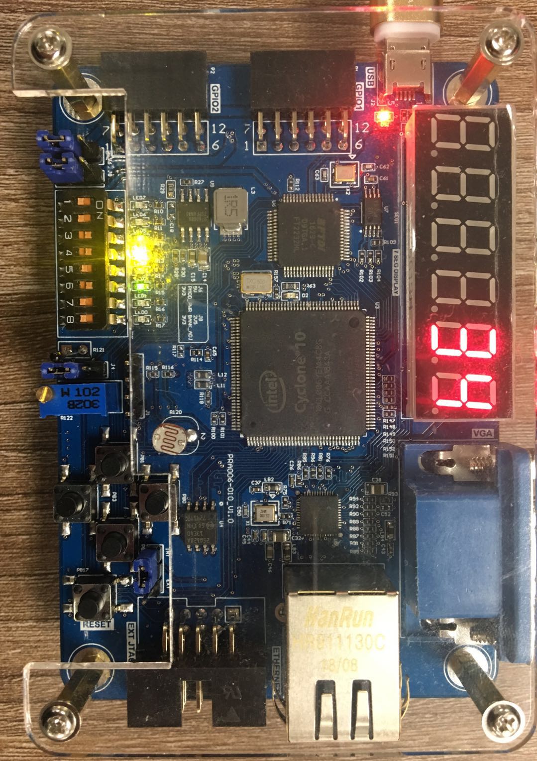
Fig 11. 3 Demonstration of develop board