FPGA Tutorial – Asynchronous Serial Port Design and Experiment – FPGA for Beginner – Experiment 10
Experiment 10 Asynchronous Serial Port Design and Experiment
10.1 Experiment Objective
- Because asynchronous serial ports are very common in industrial control, communication, and software debugging, they are also vital in FPGA development.
- Learning the basic principles of asynchronous serial port communication, handshake mechanism, data frame
- Master asynchronous sampling techniques
- Review the frame structure of the data packet
- Learning FIFO
- Joint debugging with common debugging software of PC (SSCOM, teraterm, etc.)
10.2 Experiment Requirement
- Design and transmit full-duplex asynchronous communication interface Tx, Rx
- Baud rate of 11520 bps, 8-bit data, 1 start bit, 1 or 2 stop bits
- Receive buffer (Rx FIFO), transmit buffer (Tx FIFO)
- Forming a data packet
- Packet parsing
10.3 Experiment
- Build new project named uart_frame, select 10Cl010YF144C8G for device.
- Add new file named uart_top, add a PLL (can be copied from the previous experiment)
module uart_top
(
input inclk,
input rst,
Input baud_sel,
input rx,
output intx
);
wire sys_clk;
wire uart_clk;
wire sys_rst;
wire uart_rst;
pll_sys_rst pll_sys_rst_inst
(
.inclk (inclk),
.sys_clk (sys_clk),
.uart_clk (uart_clk),
.sys_rst (sys_rst),
.uart_rst(uart_rst)
);
endmodule
- New baud rate generator file
- Input clock 7.3728MHz (64 times 115200). The actual value is 7.377049MHz, which is because the coefficient of the PLL is an integer division, while the error caused by that is not large, and can be adjusted by the stop bit in asynchronous communication. See Fig 10. 1.
Fine solution
Implemented with a two-stage PLL for a finer frequency
-
-
- The stop bit is set to be 2 bits, which can effectively eliminate the error.
-
This experiment will not deal with the precision. The default input frequency is 7.3728 MHz.
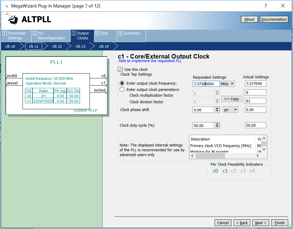
Fig 10. 1 PLL setting
- Supported baud rates are 115200,57600,38400,19200
- The default baud rate is 115200
- Design of baud rate (Refer to the project files UART_FRAME)
- Instantiate and set it as top level
wire tx_band;
Wire tx_band;
baud_rate
#(.div(64))
baud_rate_inst
(
.rst (uart_rst),
.inclk (uart_clk),
.baud_sel (baud_sel),
.baud_tx (baud_tx),
);
- Baud rate design source file
module baud_rate
#(parameter div=64)
(
input rst,
input inclk,
input [1:0] baud_sel,
output reg baud_tx,
output reg baud_rx
);
wire [8:0] frq_div_tx; //Send baud rate, clock frequency division selection
assign frq_div_tx=(baud_sel==2’b0)?9’d63:
(baud_sel==2’b01)?9’d127:
(baud_sel==2’b10)?9’d255:9’d511;
reg [8:0] count_tx=9’d0;
always@(posedge inclk)
if(rst) begin
count_tx <=9’d0;
baud_tx <=1’b0;
end
else begin
if(count_tx==frq_div_tx) begin
count_tx <=9’d0;
baud_tx<=1’b1;
end
else begin
count_tx<=count_tx+1’b1;
baud_tx<=1’b0;
end
end
wire [6:0] frq_div_rx; //Accept partial baud rate design
assign frq_div_rx=(baud_sel==2’b0)?7’d7:
(baud_sel==2’b01)?7’d15:
(baud_sel==2’b10)?7’d31:7’d63;
reg [8:0] count_rx=9’d0;
always@(posedge inclk)
if(rst) begin
count_rx <=9’d0;
baud_rx <=1’b0;
end
else begin
if(count_rx==frq_div_rx) begin
count_rx <=9’d0;
baud_rx<=1’b1;
end
else begin
count_rx<=count_rx+1’b1;
baud_rx<=1’b0;
end
end
endmodule
- Design the buffer file tx_buf
- 8-bit FIFO, depth is 256, read/write clock separation, full flag, read empty flag
- Interface and handshake
-
- rst reset signal
- wr_clk write clock
- tx_clk send clock
- 8-bit write data tx_data
- wr_en write enable
- ctrl writes whether the data is a data or a control word
- rdy buffer ready, can accept the next data frame
-
- Send buffer instantiation file
tx_buf
#(.TX_BIT_LEN(8),.STOP_BIT(2))
tx_buf_inst
(
.sys_rst (sys_rst),
.uart_rst (uart_rst),
.wr_clk (sys_clk),
.tx_clk (uart_clk),
.tx_baud (tx_baud),
.tx_wren (tx_wren),
.tx_ctrl (tx_ctrl),
.tx_datain (tx_data),
.tx_done (tx_done),
.txbuf_rdy (txbuf_rdy),
.tx_out (tx_out)
);
- Send buffer source file (Refer to the project file)
- Serial transmission, interface and handshake file design
- Interface design
-
- tx_rdy, send vacancy, can accept new 8-bit data
- tx_en, send data enable, pass to the sending module 8-bit data enable signal
- tx_data, 8-bit data to be sent
- tx_clk, send clock
- tx_baud, send baud rate
-
- Instantiation
tx_transmit
#(.DATA_LEN(TX_BIT_LEN),
.STOP_BIT(STOP_BIT)
)
tx_transmit_inst
(
.tx_rst (uart_rst),
.tx_clk (tx_clk),
.tx_baud (tx_baud),
.tx_en (tx_en),
.tx_data (tx_data),
.tx_rdy (trans_rdy),
.tx_out (tx_out)
);
- Source file (Refer to the project files)
- Send file testbench.v (Refer to the project file tb_uart)
- Send ModelSim simulation. See Fig 10. 2 (Already saved as wave.do file)
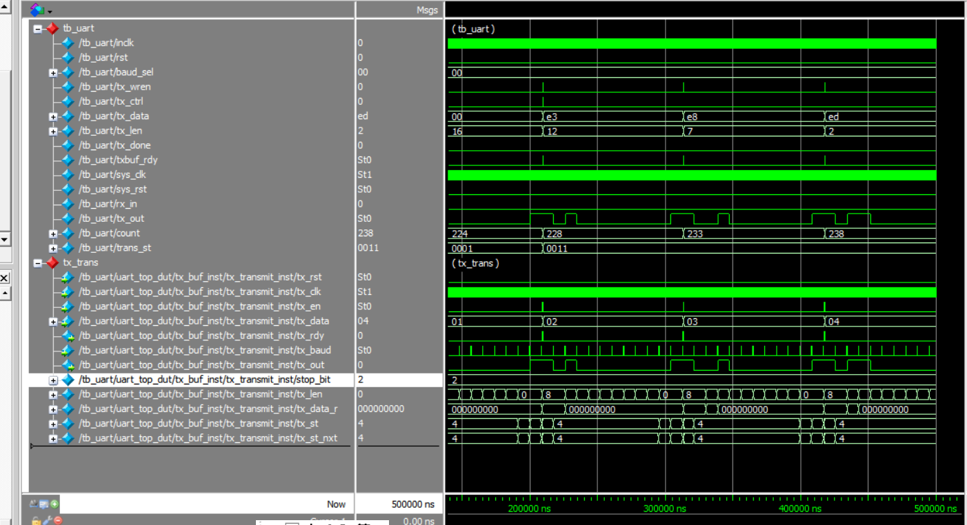
Fig 10. 2 ModelSim simulation waves sent by serial
- Extended design (extended content is only reserved for users to think and practice)
- Design the transmitter to support 5, 6, 7, 8-bit PHY (Port physical layer)
- Support parity check
- The settings of the above steps involve FIFO, PLL, etc. (Refer to uart_top project file)
UART accept file design
- Design of rx_phy.v
Design strategies and steps
Use 8 times sampling: so rx_baud is different from tx_baud, here sampling is rx_band = 8*tx_band
Adopting multiple judgments to realize the judgment of receiving data. Determine whether the data counter is greater than 4 after the sampling value is counted.
-
-
- Steps to receive data:
-
- Synchronization: refers to how to find the start bit from the received 0101… sync_dtc
- Receive start bit (start)
- Cyclically receive 8-bit data
- Receive stop bit (determine whether it is one stop bit or two stop bits)
Determine if the stop bit is correct
Correct, jump to step ii
Error, jump to step i, resynchronize
Do not judge, jump directly ii, this design adopts the scheme of no judgment
- rx_phy source file (Refer to the project file)
- The design of rx_buf
Design strategies and steps
Add 256 depth, 8-bit fifo
- Read and write clock separation
- Asynchronous clear (internal synchronization)
- Data appears before the rdreq in the read port
Steps:
- Initialization: fifo, rx_phy
- Wait: FIFO full signal (wrfull) is 0
- Write: Triggered by rx_phy: rx_phy_byte, rx_phy_rdy
- End of writing
- Back to ii and continue to wait
rx_buf.v source program (Reference to project files)
Receive simulation incentive
Content and steps
- tx, rx loopback test (assign rx_in = tx_out)
- Continue to use the incentive file in the TX section
- Writing the incentive part of rx
Modelsim simulation, as shown in Fig 10. 3
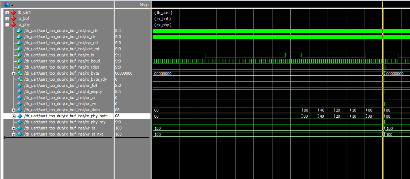
Fig 10. 3 ry_phy waveform
Reflection and expansion
- Modify the program to complete the 5, 6, 7, 8-bit design
- Completing the design of the resynchronization when the start and stop have errors of the receiving end rx_phy
- Complete the analysis and packaging of the receipt frame of rx_buf
- Using multi-sampling to design 180° alignment of data, compare with FPGA resources, timing and data recovery effects
Hardware test
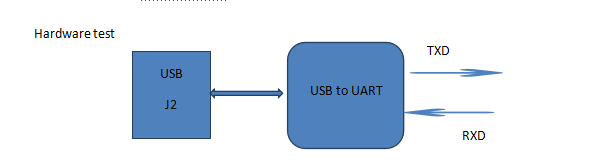
Fig 10. 4 USB to serial conversion
Firstly, Use FII-PR006 to test
Secondly, FPGA and UART pin mapping table. See Table 10. 1
| UART | RXD | TXD |
| Schematic Name | JTAG_TXD_O | JTAG_RXD_I |
| FPGA Pin | 144 | 143 |
Table 10. 1 FPGA and UART pin mapping table
Thirdly, lock the pins, and recompile
Fourthly, write a hardware test file
- Development board J2 is connected to the host USB interface
- Using test software such as teraterm, SSCOM3, etc. You can also write a serial communication program (C#, C++, JAVA, Python…).
- PC sends data in a certain format
- The test end uses a counter to generate data in a certain format.
- The test procedure is as follows (hw_tb_uart)
module hw_tb_uart(
input inclk,
input rst,
input rx_in,
output tx_out
);
wire [1:0] baud_sel=2’b00; //Default baud rate is 115200
reg tx_wren=0;
reg tx_ctrl=0;
reg [7:0] tx_data=0;
reg [7:0] tx_len=0;
reg tx_done;
wire txbuf_rdy;
wire sys_clk;
wire sys_rst;
reg [7:0] count=0;
reg [3:0] trans_st;
always@(posedge sys_clk)
if(sys_rst)begin
trans_st <=0;
tx_wren <=1’b0;
tx_ctrl <=1’b0;
tx_data <=8’b0;
tx_done <=1’b0;
tx_len <=0;
tx_len <=0;
count <=8’d0;
end
else case(trans_st)
0:begin
trans_st <=1;
tx_wren <=1’b0;
tx_ctrl <=1’b0;
tx_data <=8’b0;
tx_done <=1’b0;
tx_len <=16;
end
1:begin
tx_wren <=1’b0;
tx_ctrl <=1’b0;
tx_data <=8’b0;
tx_done <=1’b0;
if(txbuf_rdy)
trans_st <=2;
end
2:begin
tx_wren <=1’b1;
tx_ctrl <=1’b1;
tx_data <=tx_len;
trans_st <=3;
end
3:begin
tx_wren <=1’b0;
tx_ctrl <=1’b0;
if(tx_len==0)
trans_st <=4;
else if(txbuf_rdy) begin
tx_data <=count;
count <=count+1;
tx_wren <=1’b1;
tx_len <=tx_len-1;
end
end
4:begin
tx_wren <=1’b0;
tx_ctrl <=1’b0;
tx_data <=0;
tx_len <=16;
tx_done <=1’b1;
trans_st <=5;
end
5:begin
tx_done <=1’b0;
trans_st <=1;
end
endcase
wire [7:0] rx_byte;
wire rx_byte_rdy;
reg [7:0] rx_byte_r;
reg rx_rden;
always@(posedge sys_clk)
if(rx_byte_rdy)begin
rx_rden <=1’b1;
rx_byte_r<=rx_byte;
end
else begin
rx_rden<=1’b0;
end
uart_top uart_top_dut
(
.inclk (inclk),
.rst (rst),
.baud_sel (baud_sel),
.tx_wren (tx_wren),
.tx_ctrl (tx_ctrl),
.tx_data (tx_data),
.tx_done (tx_done),
.txbuf_rdy (txbuf_rdy),
.rx_rden (rx_rden),
.rx_byte (rx_byte),
.rx_byte_rdy(rx_byte_rdy),
.sys_clk (sys_clk),
.sys_rst (sys_rst),
.rx_in (rx_in),
.tx_out (tx_out)
);
endmodule
Set this file to be top level entity and instantiate the previous program. Download the program to the board and verify it.
Fifthly, lock the pins and test.
| Signal Name | Port Description | Network Label | FPGA Pin |
| Inclk | Clock input | C10_50MCLK | 91 |
| rst | Reset signal | KEY2 | 10 |
| rx_in | Serial input data | TAG_RXD_I | 144 |
| tx_out | Serial output data | TAG_TXD_O | 143 |
Observe the data received by PC. See Fig 10. 5
Use SignalTap II to observe the data received by FPGA.
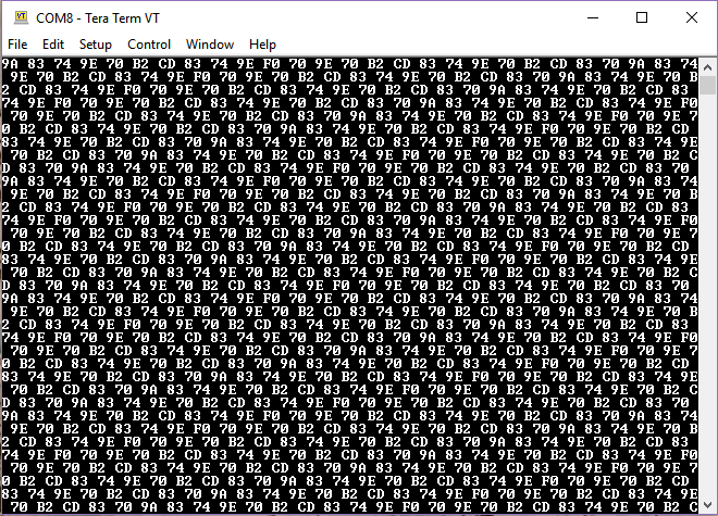
Fig 10. 5 Data sent displayed on the host computer
Sixthly, the receiving part has been eliminated here. You are encouraged to try it on your own.