Use Dual-port RAM to Read and Write Frame Data, use synchronous (or asynchronous ) clock to control the synchronization of frame structure – FPGA Board Beginner Tutorial – Experiment 9
Experiment 9 Use Dual_port RAM to Read and Write Frame Data
9.1 Experiment Objective
- Learn to configure and use dual-port RAM
- Learn to use synchronous clock to control the synchronization of frame structure
- Learn to use asynchronous clock to control the synchronization of frame structure
Experiment Implement
- Observing the synchronization structure of synchronous clock frames using SignalTap II
- Extended the use of dual-port RAM
- Design the use of three-stage state machine
- Design a 16-bit data frame
- Data is generated by an 8-bit counter: Data={~counta,counta}
- The ID of the data frame inputted by the switch (7 bits express maximum of 128 different data frames)
- 16-bit checksum provides data verification
- 16-bit checksum accumulates, discarding the carry bit
- After the checksum is complemented, append to the frame data
- Provide configurable data length data_len by parameter
- Packet: When the data and checksum package are written to the dual-port RAM, the userID, the frame length and the valid flag are written to the specific location of the dual-port RAM. The structure of the memory is shown in Table 9.1.
| Wr_addr | Data/Flag | Rd_addr |
| 8’hff | {valid,ID,data_len} | 8’hff |
| … | N/A | … |
| 8’hnn+2 | N/A | 8’hnn+2 |
| 8’hnn+1 | ~checksum+1 | 8’hnn+1 |
| 8’hnn | datann | 8’hnn |
| … | …. | … |
| 8’h01 | Data1 | 8’h01 |
| 8’h00 | Data0 | 8’h00 |
Table 1 Memory Structure
6. Read and write in an agreed order
Valid is the handshake signal. This flag provides the possibility of read and write synchronization, so the accuracy of this signal must be ensured in the program design.
9.3 Experiment
9.3.1 Introduction of the Program
The first step: the establishment of the main program framework
module frame_ram
#(parameter data_len=250)
(
input inclk,
input rst,
input [6:0] sw,
output reg [6:0] oID,
output reg rd_done,
output reg rd_err
);
The second step: the definition of the state machine
parameter [2:0] mema_idle=0,
mema_init=1,
mema_pipe0=2,
mema_read0=3,
mema_read1=4,
mema_wr_data=5,
mema_wr_chsum=6,
mema_wr_done=7;
parameter [2:0] memb_idle=0,
memb_init=1,
memb_pipe0=2,
memb_read0=3,
memb_read1=4,
memb_rd_data=5,
memb_rd_chsum=6,
memb_rd_done=7;
The third step: other definitions
Clock variable definition

wire sys_clk;

wire BCD_clk;

wire sys_rst;

reg ext_clk;

Dual-port RAM interface definition

reg [7:0] addr_a;

reg [15:0] data_a;

reg wren_a;

wire [15:0] q_a;

reg [7:0] addr_b;

reg wren_b;

wire [15:0] q_b;

Write state machine part variable definition

reg [6:0] user_id;

reg [7:0] wr_len;

reg [15:0] wr_chsum;

wire wr_done;

reg [7:0] counta;

wire [7:0] countb;

assign countb=~counta;

reg [15:0] rd_chsum;

reg [7:0] rd_len;

reg [15:0] rd_data;

reg ext_rst;

reg [2:0] sta;

reg [2:0] sta_nxt,;

Read state machine part variable definition

reg [15:0] rd_chsum;

reg [7:0] rd_len;

reg [15:0] rd_data;

reg [2:0] stb;

reg [2:0] stb_nxt;
The fourth step: generate dual-port RAM, PLL
dp_ram dp_ram_inst

(

.address_a (addr_a),

.address_b (addr_b),

.clock (sys_clk),

.data_a (data_a),

.data_b (16'b0),

.wren_a (wren_a),

.wren_b (wren_b),

.q_a (q_a),

.q_b (q_b)

);

pll_sys_rst pll_sys_rst_inst

(

.inclk (inclk),

.sys_clk (sys_clk),

.BCD_clk (BCD_clk),

.sys_rst (sys_rst)

);
The RAM is 16 bits wide and 256 depth. The PLL inputs a 50 MHz clock, outputs 100 MHz as the operating clock of other modules, and 20 MHz is used to drive the segment display.
The fifth step: data generation counter
always @ (posedge sys_clk)

if(sys_rst) begin

counta <= 0;

user_id <= 0;

end

else begin

counta <=counta + 1;

user_id <= sw;

end
The sixth step: write state machine
assign wr_done = (wr_len == (data_len - 1'b1));

//Think why using wr_len==data_len-1, instaed of wr_len==data_len

//First stage

always @ (posedge sys_clk)

begin

if (sys_rst) begin

sta = mema_idle;

end

else

sta = sta_nxt;

end

//Second stage

always @ (*)

begin

case (sta)

mema_idle : sta_nxt = mema_init;

mema_init : sta_nxt = mema_pipe0;

mema_pipe0 : sta_nxt = mema_read0;

mema_read0 :

begin

if (!q_a[15])

sta_nxt = mema_read1;

else

sta_nxt = sta;

end

mema_read1 :

begin

if (!q_a[15])

sta_nxt = mema_wr_data;

else

sta_nxt = sta;

end

mema_wr_data :

begin

if (wr_done)

sta_nxt = mema_wr_chsum;

else

sta_nxt = sta;

end

mema_wr_chsum : sta_nxt = mema_wr_done;

mema_wr_done : sta_nxt = mema_init;

default : sta_nxt = mema_idle;

endcase

end  //Third stage

always @ (posedge sys_clk)

begin

case (sta)

mema_idle :

begin

addr_a <= 8'hff;

wren_a <= 1'b0;

data_a <= 16'b0;

wr_len <= 8'b0;

wr_chsum <= 0;

end

mema_init, mema_pipe0, mema_read0, mema_read1 :

begin

addr_a <= 8'hff;

wren_a <= 1'b0;

data_a <= 16'b0;

wr_len <= 8'b0;

wr_chsum <= 0;

end

mema_wr_data :

begin

addr_a <= addr_a + 1'b1;

wren_a <= 1'b1;

data_a <= {countb, counta};

wr_len <= wr_len + 1'b1;

wr_chsum <= wr_chsum + {countb, counta};

end

mema_wr_chsum :

begin

addr_a <= addr_a + 1'b1;

wr_len <= wr_len + 1'b1;

wren_a <= 1'b1;

data_a <= (~wr_chsum) + 1'b1;

end

mema_wr_done :

begin

addr_a <= 8'hff;

wren_a <= 1'b1;

data_a <= {1'b1, user_id, wr_len};

end

default : ;

endcase

end
Write order:
- Read the flag of the 8’hff address (control word). If valid=1’b0, the program proceeds to the next step, otherwise waits
- Address plus 1, 8’hff+1 is exactly zero, write data from 0 address and calculate the checksum
- Determine whether the predetermined data length is reached. If so, proceeds to next step, otherwise continue writing data, and the checksum is calculated.
- checksum complements and write to memory
- Write the control word in the address 8’hff, packet it
The seventh step: read state machine
//First stage

always @ (posedge sys_clk)

begin

if (ext_rst) begin

stb = memb_idle;

end

else

stb = stb_nxt;

end

//Second stage

always @ (*)

begin

case (stb)

memb_idle : stb_nxt = memb_init;

memb_init : stb_nxt = memb_pipe0;

memb_pipe0 : stb_nxt = memb_read0;

memb_read0 :

begin

if (q_b[15])

stb_nxt = memb_read1;

else

stb_nxt = memb_init;

end

memb_read1 :

begin

if (q_b[15])

stb_nxt = memb_rd_data;

else

stb_nxt = memb_init;

end

memb_rd_data :

begin

if(rd_done)

stb_nxt = memb_rd_chsum;

else

stb_nxt = stb;

end

memb_rd_chsum : stb_nxt = memb_rd_done;

memb_rd_done : stb_nxt = memb_init;

default : stb_nxt = memb_idle;

endcase

end

// Third stage, the actual operation needs to be driven by the edge of the clock.

always @ (posedge sys_clk)

begin

case (stb)

memb_idle :

begin

addr_b <= 8'hff;

rd_data <= 0;

rd_chsum <= 0;

wren_b <= 1'b0;

rd_len <= 8'b0;

oID <= 7'b0;

rd_err <= 1'b0;

end

memb_init :

begin

addr_b <= 8'hff;

rd_data <= 0;

rd_chsum <= 0;

wren_b <= 1'b0;

rd_len <= 8'b0;

oID <= 7'b0;

rd_err <= 1'b0;

end

memb_pipe0 :

begin

addr_b <= 8'b0;

end

memb_read0 :

begin

if (q_b[15])

addr_b <= addr_b + 1'b1;

else

addr_b <= 8'hff;

rd_data <= 0;

rd_chsum <= 0;

wren_b <= 1'b0;

rd_len <= 8'b0;

oID <= 7'b0;

end

memb_read1 :

begin

if(q_b[15])

addr_b <= addr_b + 1'b1;

else

addr_b <= 8'hff;

rd_data <= 0;

rd_chsum <= 0;

wren_b <= 1'b0;

rd_len <= q_b[7:0];

oID <= q_b[14:8];

end

memb_rd_data :

begin

addr_b <= addr_b + 1'b1;

rd_data <= q_b;

rd_chsum <= rd_chsum + rd_data;

wren_b <= 1'b0;

rd_len <= rd_len - 1'b1;

end

memb_rd_chsum :

begin

addr_b <= 8'hff;

wren_b <= 1'b0;

if (|rd_chsum)

rd_err <= 1'b1;

end

memb_rd_done :

begin

addr_b <= 8'hff;

wren_b <= 1'b1;

end

default : ;

endcase

end
Read order
- Idle is the state after reset
- Init: Initialization, set the address to 8’hff
- Rd_pipe0: Add a latency (since the read address and data are both latched). Address +1, forming a pipeline structure
- Read0: Set the address to 8’hff, read the control word and judge whether the valid bit is valid.
- If valid=1’b1, address +1, proceeds to the next step
- If valid=1’b0, it means the packet is not ready yet, the address is set to be 8’hff and returns to the init state.
- Read1: read the contro word again
- If valid=1’b1, address+1, ID and data length are assigned to the corresponding variables and proceeds to the next step
- If valid=1’b0, it means the packet is not ready yet, the address is set to 8’hff, and returns to the init state.
- Rd_data:
- Read data and pass to data variables
- Calculate checksum, data_len – 1
- Determine whether the data_len is 0
- 0: all data has been read, proceeds to the next step
- Not 0: continue the operation in current state
- rd_chsum: Read the value of checksum and calculate the last checksum. Correct the data and set the flag of rd_err
- rd_done: The last step clears the valid flag in memory and opens the write enable for the next packet
Experiment Verification
The first step: pin assignment
See Table 9.2 for the pin assignment.
Table 9.2 Frame data read and write experiment pin mapping
| Signal Name | Network Label | FPGA Pin | Port Description |
| Inclk | C10_50MCLK | 91 | Input clock |
| rst | KEY2 | 10 | Reset signal |
| sw[6] | SW6_LED6 | 76 | 7-digit DIP switch
(address input) |
| sw[5] | SW5_LED5 | 75 | |
| sw[4] | SW4_LED4 | 74 | |
| sw[3] | SW3_LED3 | 87 | |
| sw[2] | SW2_LED2 | 86 | |
| sw[1] | SW1_LED1 | 83 | |
| sw[0] | SW0_LED0 | 80 |
The second step: observe the read and write results of the dual-port RAM with SignalTap
- In order to facilitate the observation of the read and write state machine synergy results, the data length is changed to 4 here and recompile.Users can test themselves using long data.
module frame_ram

#(parameter data_len=4)

(

input inclk,

input rst,

input [6:0] sw,

output reg [6:0] oID,

output reg rd_done,

output reg rd_err

);
- Observe the simulation result
- Observe the handshake mechanism through dual-port RAM
- Determine whether the reading is started after the packet is written
- Determine whether the write packet is blocked before reading the entire packet is completed
- Observe the external interface signal and status
- rd_done, rd_err
Set rd_err = 1, or the rising edge is the trigger signal to observe whether the error signal is captured.
- Observe whether wren_a, wren_b signal and the state machine jump are strictly matched to meet the design requirements.
- SignalTap result. See Figure 9.1.
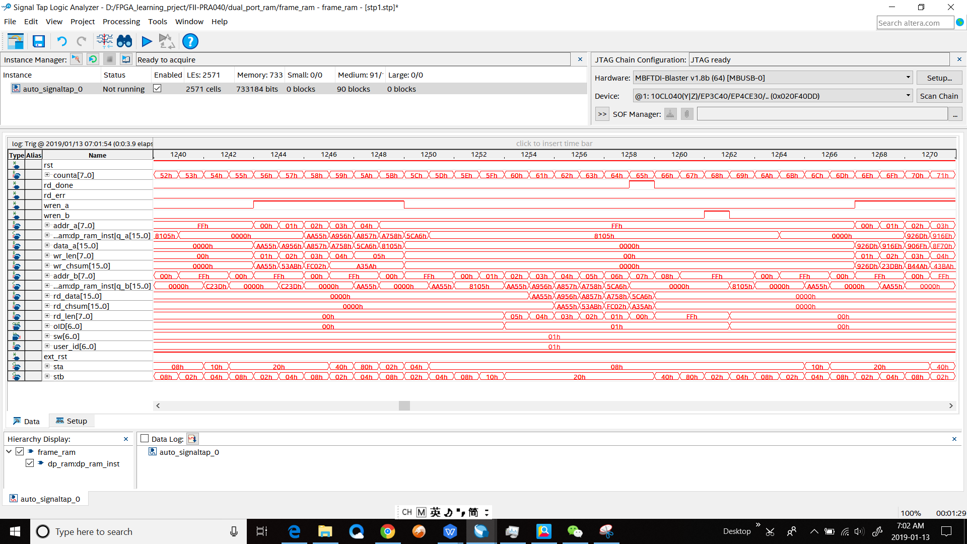
Figure 9.1 SignalTap II simulation
Experiment Summary and Reflection
- Review the design requirements of how to analyze an actual demand, to gradually establish a model of digital control and state machine and finally design it.
- Modify the third stage of the state machine into the if…else model and implement.
- Focus on thinking If the read and write clocks are different. After it becomes an asynchronous mechanism, how to control the handshake protocol.
- According to the above example, consider how dual-port RAM can be used in data acquisition, asynchronous communication, embedded CPU interface, and DSP chip interface.
- How to build ITCM with dual-port RAM and DTCM preparing for future CPU design.
————————————————————————————————-
old version (2019)
9.1 Experiment Objective
- Learn to configure and use dual-port RAM
- Learn to use synchronous clock to control the synchronization of frame structure
- Learn to use asynchronous clock to control the synchronization of frame structure
- Observing the synchronization structure of synchronous clock frames using SignalTap II
- Extended the use of dual-port RAM
- Design the use of three-stage state machine
9.2 Experiment Requirement
-
Generate dual-port RAM and PLL
-
-
16-bit width, 256-depth dual-port RAM
-
2 PLL, both 50 MHz input, different 100 MHz and 20 MHz outputs
-
-
Design a 16-bit data frame
-
-
Data is generated by an 8-bit counter: Data={~counta,counta}
-
The ID of the data frame inputted by the switch (7 bits express maximum of 128 different data frames)
-
16-bit checksum provides data verification
-
-
-
-
-
16-bit checksum accumulates, discarding the carry bit
-
After the checksum is complemented, append to the frame data
-
-
-
d. Provide configurable data length data_len by parameter
e. Packet: When the data and checksum package are written to the dual-port RAM, the userID, the frame length and the valid flag are written to the specific location of the dual-port RAM. The structure of the memory is shown in Table 9. 1
-
Wr_addr Date/ Flag Rd_addr 8’hff {valid, ID, data_len} 8’hff … N/A … 8’hnn+2 N/A 8’hnn+2 8’hnn+1 ~checksum+1 8’hnn+1 8’hnn datann 8’hnn … …. … 8’h01 Data1 8’h01 8’h00 Data0 8’h00
Table 9. 1 Memory structure
-
Read and write in an agreed order
Firstly, write in the order
-
Read the flag of the 8’hff address (control word). If valid=1’b0, the program proceeds to the next step, otherwise waits
-
Address plus 1, 8’hff+1 is exactly zero, write data from 0 address and calculate the checksum
-
Determine whether the interpretation reaches the predetermined data length. If so, proceeds to next step, otherwise the data is written, and the checksum is calculated.
-
checksum complements and write to memory
-
Write the control word in the address 8’hff, packet it
Secondly, read in the order
-
Idle is the state after reset
-
Init: Initialization, set the address to 8’hff
-
Rd_pipe0: Add a latency (since the read address and data are both latched). Address +1, forming a pipeline structure
-
Read0: Set the address to 8’hff, read the control word and judge whether the valid bit is valid.
If valid=1’b1, address +1, proceeds to the next step
If valid=1’b0, it means the packet is not ready yet, the address is set to be 8’hff and returns to the init state.
-
Read1: Read the control word again
If valid=1’b1, address+1, ID and data length are assigned to the corresponding variables and proceeds to the next step
If valid=1’b0, it means the packet is not ready yet, the address is set to 8’hff, and returns to the init state.
-
Rd_data:
Read data and pass to data variables
Calculate checksum, data_len – 1
Determine whether the data_len is 0, if so, all data has been read, proceeds to the next step, otherwise, continue the operation in current state
-
grd_chsum: Read the value of checksum and calculate the last checksum. Correct the data and set the flag of rd_err
-
rd_done: The last step clears the valid flag in memory and opens the write enable for the next packet.
Thirdly, valid is the handshake signal. This flag provides the possibility of read and write synchronization, so the accuracy of this signal must be ensured in the program design. See the project files for more details.
9.3 Experiment
- Port
module frame_ram
#(parameter data_len=250)
(
input inclk,
input rst, //external reset
input [6:0]sw, //used as input ID
output reg[6:0] oID, //used as output ID
output reg rd_done, //frame read is done
output reg rd_err //frame read has errors
);
- Definition of state machine
parameter	[2:0] mema_idle=0,
					mema_init=1,
					mema_pipe0=2,
					mema_read0=3,
					mema_read1=4,
						mema_wr_data=5,
						mema_wr_chsum=6,
						mema_wr_done=7;

	parameter	[2:0] 	memb_idle=0,
						memb_init=1,
						memb_pipe0=2,
						memb_read0=3,
						memb_read1=4,
						memb_rd_data=5,
						memb_rd_chsum=6,
						memb_rd_done=7;
- Define clock parameter
wire sys_clk;

wire BCD_clk;

wire sys_rst;

reg ext_clk;
- Define two-port RAM interface
reg [7:0] addr_a;

reg [15:0] data_a;

reg wren_a;

wire [15:0] q_a;

reg [7:0] addr_b;

reg wren_b;

wire [15:0] q_b;
- Write state machine partial variable definition
-
- Write state machine variables
reg[6:0] user_id;
reg[7:0] wr_len;
reg[15:0] wr_chsum;
wire wr_done;
reg[7:0] counta;
wire[7:0] countb=~counta;
reg ext_rst;
reg [2:0] sta;
reg[2:0] sta_nxt;
-
- Read state machine variables
reg[15:0] rd_chsum;
reg[7:0] rd_len;
reg[15:0] rd_data;
reg ext_rst;
reg[2:0] stb;
reg[2:0] stb_nxt;
- Data generation counter
always@(posedge BCD_clk)
ext_rst<=rst;
always@(posedge sys_clk)
if(sys_rst) begin
counta <=0;
user_id <=0;
end
else begin
counta <=counta+1;
user_id<=sw;
end
- Write state machine
-
- First and second stages
assign wr_done=(wr_len==data_len-1); //Think why to use wr_len==data_len-1
//instead of wr_len==data_len
always@(posedge sys_clk)
if(sys_rst) begin
sta=mema_idle;
end
else
sta=sta_nxt;
always@(*)
case (sta)
mema_idle : sta_nxt=mema_init;
mema_init : sta_nxt=mema_pipe0;
mema_pipe0 : sta_nxt=mema_read0;
mema_read0 :begin
if(!q_a[15])
sta_nxt=mema_read1;
else
sta_nxt=sta;
end
mema_read1:begin
if(!q_a[15])
sta_nxt=mema_wr_data;
else
sta_nxt=sta;
end
mema_wr_data: begin
if(wr_done)
sta_nxt=mema_wr_chsum;
else
sta_nxt=sta;
end
mema_wr_chsum: sta_nxt=mema_wr_done;
mema_wr_done: sta_nxt=mema_init;
default:sta_nxt=mema_idle;
endcase
- Third stage
always@(posedge sys_clk)
case (sta)
mema_idle: begin
addr_a<=8’hff;
wren_a<=1’b0;
data_a<=16’b0;
wr_len<=8’b0;
wr_chsum<=0;
end
mema_init,mema_pipe0,mema_read0,mema_read1: begin
addr_a<=8’hff;
wren_a<=1’b0;
data_a<=16’b0;
wr_len<=8’b0;
wr_chsum<=0;
end
mema_wr_data:begin
addr_a<=addr_a+1;
wren_a<=1’b1;
data_a<={countb,counta};
wr_len<=wr_len+1;
wr_chsum<=wr_chsum+{countb,counta};
end
mema_wr_chsum:begin
addr_a<=addr_a+1;
wr_len<=wr_len+1;
wren_a<=1’b1;
data_a<=(~wr_chsum)+1’b1;
end
mema_wr_done:begin
addr_a<=8’hff;
wren_a<=1’b1;
data_a<={1’b1,user_id,wr_len};
end
default:;
endcase
- Read state machine
-
- First stage
always@(posedge sys_clk)
if(ext_rst) begin
stb=memb_idle;
end
else
stb=stb_nxt;
-
Second stage
always @ (*)
case (stb)
memb_idle : stb_nxt=memb_init;
memb_init : stb_nxt=memb_pipe0;
memb_pipe0 : stb_nxt=memb_read0;
memb_read0 :begin
if(q_b[15])
stb_nxt=memb_read1;
else
stb_nxt=memb_init;
end
memb_read1:begin
if(q_b[15])
stb_nxt=memb_rd_data;
else
stb_nxt=memb_init;
end
memb_rd_data: begin
if(rd_done)
stb_nxt=memb_rd_chsum;
else
stb_nxt=stb;
end
memb_rd_chsum: stb_nxt=memb_rd_done;
memb_rd_done: stb_nxt=memb_init;
default:stb_nxt=memb_idle;
endcase
-
Third stage. The actual operation is driven by the edge of the clock
always@(posedge sys_clk)
case(stb)
memb_idle: begin
addr_b<=8’hff;
rd_data<=0;
rd_chsum<=0;
wren_b<=1’b0;
rd_len<=8’b0;
oID<=7’b0;
rd_err<=1’b0;
end
memb_init: begin
addr_b<=8’hff;
rd_data<=0;
rd_chsum<=0;
wren_b<=1’b0;
rd_len<=8’b0;
oID<=7’b0;
rd_err<=1’b0;
endmemb_pipe0: begin
addr_b<=8’b0;
end
memb_read0: begin
if(q_b[15])
addr_b<=addr_b+1’b1;
else
addr_b<=8’hff;
rd_data<=0;
rd_chsum<=0;
wren_b<=1’b0;
rd_len<=8’b0;
oID<=7’b0;
end
memb_read1: begin
if(q_b[15])
addr_b<=addr_b+1’b1;
else
addr_b<=8’hff;
rd_data<=0;
rd_chsum<=0;
wren_b<=1’b0;
rd_len<=q_b[7:0];
oID<=q_b[14:8];
end
memb_rd_data: begin
addr_b<=addr_b+1’b1;
rd_data<=q_b;
rd_chsum<=rd_chsum+rd_data;
wren_b<=1’b0;
rd_len<=rd_len-1’b1;
end
memb_rd_chsum: begin
addr_b<=8’hff;
wren_b<=1’b0;
if(|rd_chsum)//Determine if rd_chsum is not 0, error occurs when reading data
rd_err<=1’b1;
end
memb_rd_done: begin
addr_b<=8’hff;
wren_b<=1’b1;
end
default:;
endcase
always@(*)begin
if(stb==memb_rd_data)
rd_done=(rd_len==0);
else
rd_done=1’b0;
end
- Instantiate dual-port RAM and PLL
//Instantiate dual-port RAM
dp_ram dp_ram_inst
(
.address_a(addr_a),
.address_b(addr_b),
.clock (sys_clk),
.data_a (data_a),
.data_b (16’b0),
.wren_a (wren_a),
.wren_b(wren_b),
.q_a (q_a),
.q_b (q_b)
);
//Instantiate PLL
pll_sys_rst pll_sys_rst_inst
(
.inclk (inclk),
.sys_clk (sys_clk),
.BCD_clk(BCD_clk),
.sys_rst (sys_rst)
);
endmodule
9.4 Lock the Pins, Compile, and Download to FII-PRA006 FPGA to Test
|
Signal Name |
Port Description |
Network Label |
FPGA Pin |
|
Inclk |
Input clock |
C10_50MCLK |
91 |
|
rst |
Reset signal |
KEY2 |
10 |
|
sw[6] |
Switch input 6 |
SW6_LED6 |
76 |
|
sw[5] |
Switch input 5 |
SW5_LED5 |
75 |
|
sw[4] |
Switch input 4 |
SW4_LED4 |
74 |
|
sw[3] |
Switch input 3 |
SW3_LED3 |
87 |
|
sw[2] |
Switch input 2 |
SW2_LED2 |
86 |
|
sw[1] |
Switch input 1 |
SW1_LED1 |
83 |
|
sw[0] |
Switch input 0 |
SW0_LED0 |
80 |
9.5 Use SignalTap II to Observe the Dual-port RAM Read and Write
-
-
-
-
In order to facilitate the observation of the read and write state machine synergy results, the data length is changed to 4 here, recompile and download. Users can test themselves using long data.
-
-
-
module frame_ram
#(parameter data_len=4)
(
input inclk,
input rst, //external reset
input [6:0]sw, //used as input ID
output reg[6:0] oID, //used as output ID
output reg rd_done, //frame read is done
output reg rd_err //frame read has errors
);
-
-
-
- SignalTap II simulation result. See Fig 9. 1
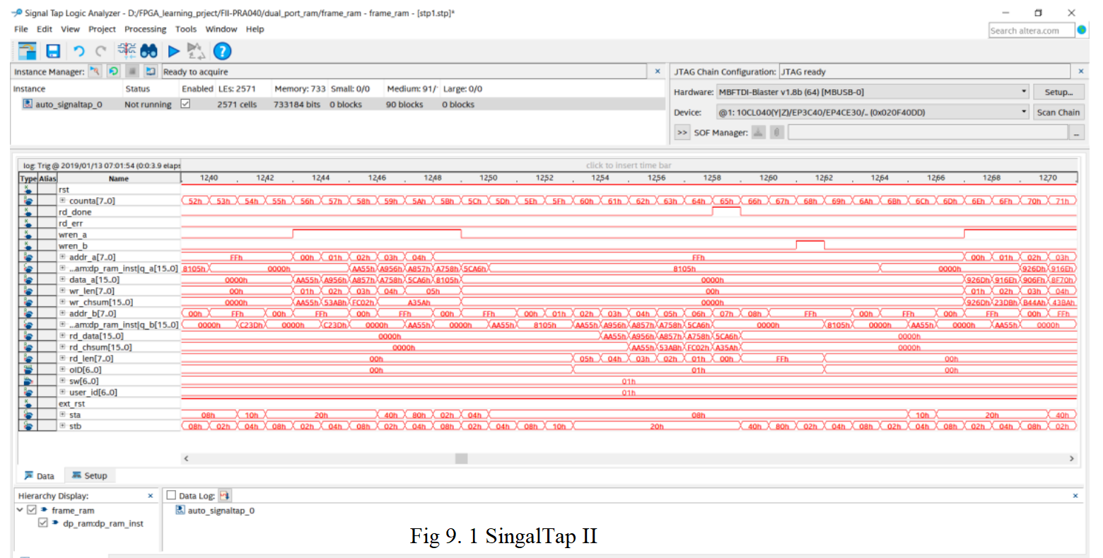
singal Tap
- SignalTap II simulation result. See Fig 9. 1
-
-
Fig 9. 1 SingalTap II simulation
-
-
-
-
Observe the simulation result
-
-
-
-
Observe the handshake mechanism through dual-port RAM
Determine whether the reading is started after the packet is written, whether the write packet is blocked before reading the entire packet is completed.
-
Observe the external interface signal and status
Rd_done, rd_err
Set rd_err = 1, or the rising edge is the trigger signal to observe whether the error signal is captured.
Observe whether wren_a, wren_b signal and the state machine jump are strictly matched to meet the design requirements.
9.6 Experiment Summary and Reflection
-
-
-
-
-
-
-
Review the design requirements. How to analyze an actual demand, gradually establish a model of digital control and state machine and finally design.
-
Modify the third stage of the state machine into the if…else model and implement.
-
Focus on thinking If the read and write clocks are different, it becomes an asynchronous mechanism, how to control the handshake.
-
According to the above example, consider how dual-port RAM can be used in data acquisition, asynchronous communication, embedded CPU interface, and DSP chip interface.
-
How to build ITCM with dual-port RAM and DTCM preparing for future CPU design.
-
-
-
-
-
-