Experimental Manuals FII-PRA040 FPGA Board Based Risc-V

SOPC (NiosII) system, simulation and verification of RISC-V CPU, Basic FPGA design training, IC design and verification – Altera Risc-V Board Tutorial : Introduction of FII-PRA040 Development System

1、Design Objective of the System The main purpose of this system design is to complete FPGA learning, development and experiment with Intel Quartus. The main device uses the Inte Cyclone10 10CL040YF484C8G and is currently the latest generation of FPGA devices from Intel. The major learning and development projects can be completed as follows: Basic FPGA design training Construction and training of the SOPC (NiosII) system IC design and verification, the system provides hardware design, simulation and verification of RISC-V CPU Development and application based on RISC-V The system is specifically…

Read More
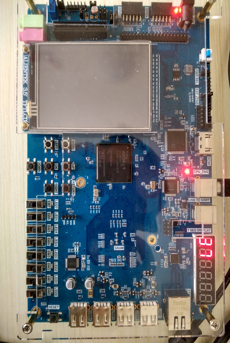
HDMI connection block diagram
Experimental Manuals FPGA Tutor PRX100 Risc-V

Understand the register configuration of the ADV7511, HDMI Graphic Display Experiment – Xilinx Risc-V Board Tutorial : FII-PRX100 FPGA Board Experiment 14

Experiment 14 HDMI Graphic Display Experiment 1.Experiment Objective Learn about video timing (2) Understand the register configuration of the ADV7511, reviewing the knowledge from experiment 12 2.Experiment Requirement Image display processing has always been the focus of FPGA research. At present, the image display mode is also developing. The image display interface is also gradually transitioning from the old VGA interface to the new DVI or HDMI interface. Display the image using the HDMI interface of the development board. Download the program to the board for comparison. Introduction to HDMI:…

Read More
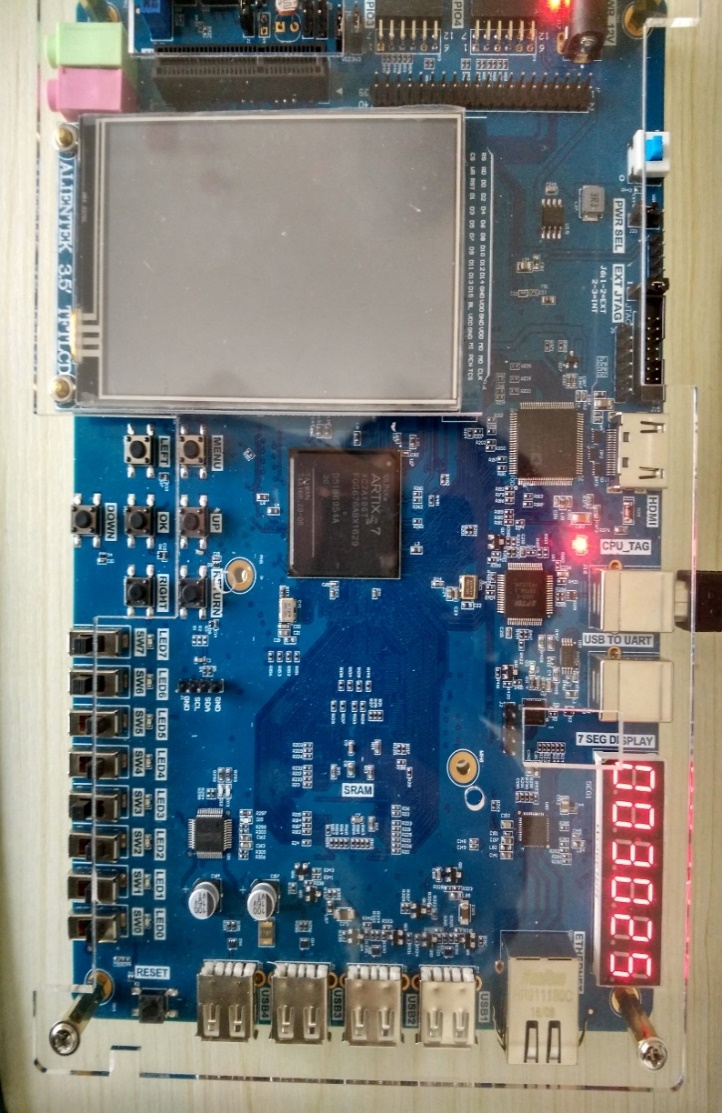
AD, DA Experiment Results
Experimental Manuals FPGA Tutor PRX100 Risc-V

digital-to-analog conversion: DAC, analog-to-digital conversion: ADC – Xilinx Risc-V Board Tutorial : AD, DA Experiment – FII-PRX100 FPGA Board Experiment 13

Experiment 13 AD, DA Experiment 1.Experiment Objective Since in the real world, all naturally occurring signals are analog signals, and all that are read and processed in actual engineering are digital signals. There is a process of mutual conversion between natural and industrial signals (digital-to-analog conversion: DAC, analog-to-digital conversion: ADC). The purpose of this experiment is twofold: Learning the theory of AD conversion Read the value of AD acquisition from PCF8591, and convert the value obtained into actual value, display it with segment decoders 2.Experiment Requirement Perform analog-to-digital conversion using…

Read More
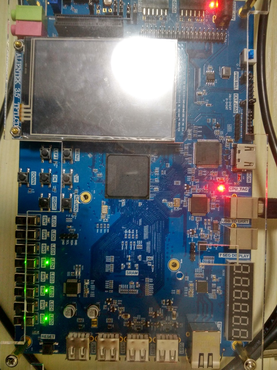
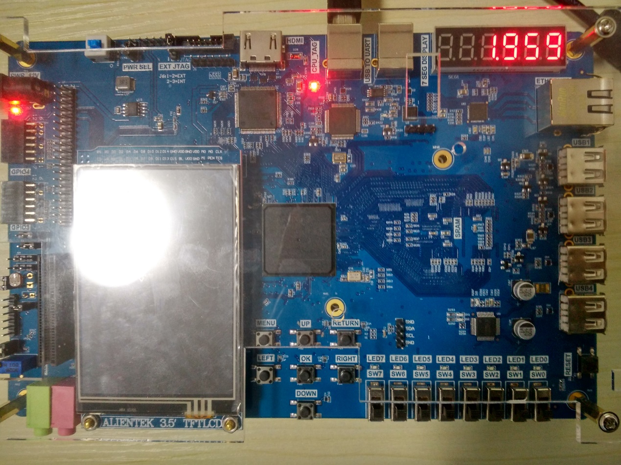
Demonstration of the develop board
Experimental Manuals FPGA Tutor PRX100 Risc-V

Learning the basic principles of the different IIC bus, mastering the IIC communication protocol, Xilinx Risc-V Board Tutorial : IIC Protocol Transmission – FII-PRX100 FPGA Board Experiment 12

Experiment 12 IIC Protocol Transmission 1.Experiment Objective There is an IIC interface EEPROM chip 24LC02 in the test plate, capacity sized 2 kbit (256 bite). Since the data is not lost after the EEPROM is powered down, users can store some hardware setup data or user information. Learning the basic principles of the different IIC bus, mastering the IIC communication protocol Master the method of reading and writing EEPROM Joint debugging using logic analyzer 2.Experiment Requirement Correctly write a number to any address in the EEPROM (this experiment writes to…

Read More
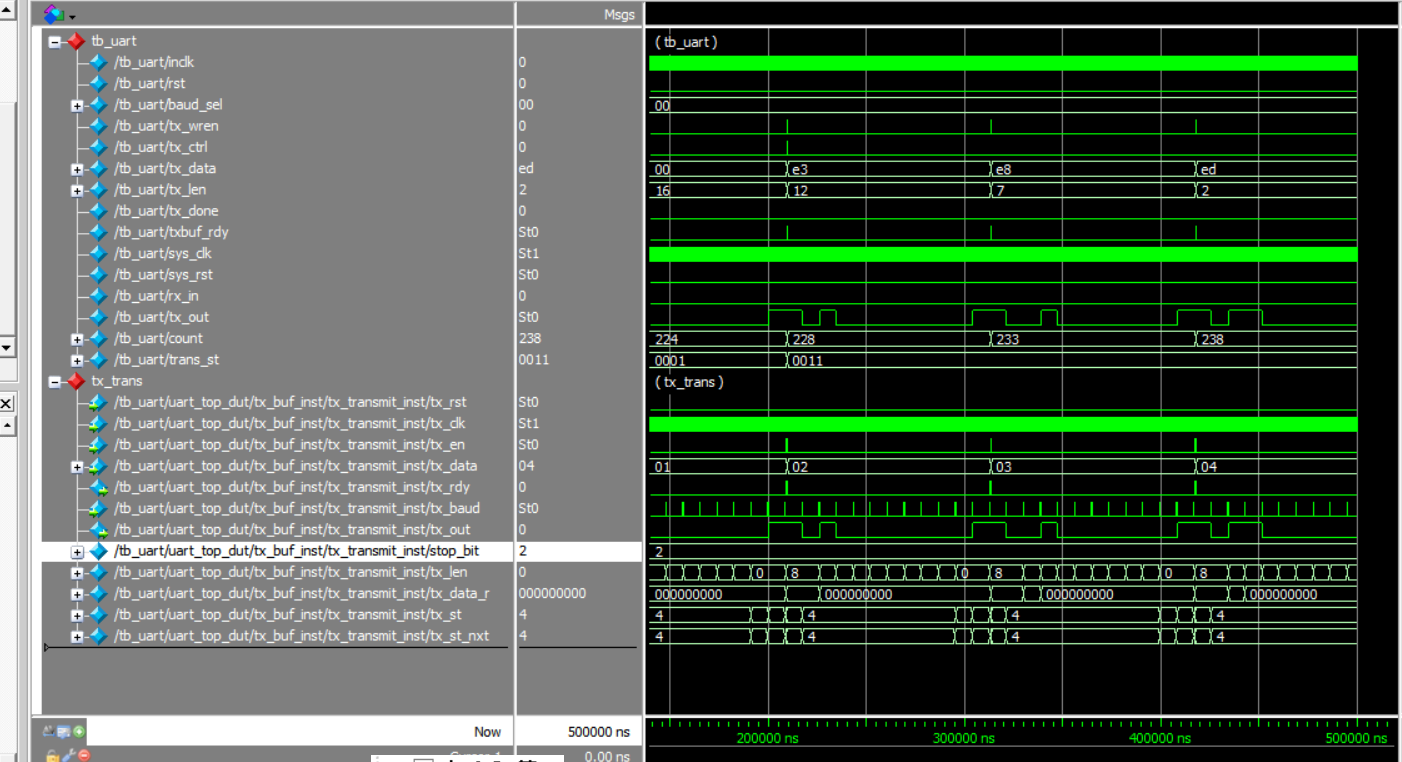
ModelSim simulation waves sent by serial
Experimental Manuals FPGA Tutor PRX100 Risc-V

Xilinx Risc-V Board Tutorial : Asynchronous Serial Port Design and Experiment – FII-PRX100 FPGA Board Experiment 11

Experiment 11 Asynchronous Serial Port Design and Experiment 1.Experiment Objective Because asynchronous serial ports are very common in industrial control, communication, and software debugging, they are also vital in FPGA development. Learning the basic principles of asynchronous serial port communication, handshake mechanism, data frame Master asynchronous sampling techniques Review the frame structure of the data packet Learning FIFO Joint debugging with common debugging software of PC (SSCOM, teraterm, etc.) 2.Experiment Requirement Design and transmit full-duplex asynchronous communication interface Tx, Rx Baud rate of 11520 bps, 8-bit data, 1 start bit,…

Read More
Risc-V Board - Dual_port RAM test result
Experimental Manuals FPGA Tutor PRX100 Risc-V

Xilinx Risc-V Board Tutorial : Use Dual_port RAM to Read and Write Frame Data – FII-PRX100 FPGA Board Experiment 10

Experiment 10 Use Dual_port RAM to Read and Write Frame Data 1.Experiment Objective Learn to configure and use dual-port RAM Learn to use synchronous clock to control the synchronization of frame structure Learn to use asynchronous clock to control the synchronization of frame structure Observing the synchronization structure of synchronous clock frames using ILA Extended the use of dual-port RAM Design the use of three-stage state machine 2.Experiment Requirement Generate dual-port RAM and PLL 16-bit width, 256-depth dual-port RAM 2 PLL, both 50 MHz input, different 100 MHz and 20…

Read More
Risc-V Use of ROM Results
Experimental Manuals FPGA Tutor PRX100 Risc-V

Study the internal memory block of FPGA, Study the format of *.mif and how to edit *.mif file to configure the contents of ROM : Use of ROM – FII-PRX100 Risc-V FPGA Board Experiment 9

Experiment 9 Use of ROM 1.Experiment Objective Study the internal memory block of FPGA Study the format of *.mif and how to edit *.mif file to configure the contents of ROM Learn to use RAM, read and write RAM 2.Experiment Design Design 16 outputs ROM, address ranging 0-255 Interface 8-bit switch input as ROM’s address Segment decoders display the contents of ROM and require conversion of hexadecimal to BCD output. 3.Design Procedure Create a coe file. This experiment *.coe file is generated based on Matlab2018. The *.m file is as…

Read More
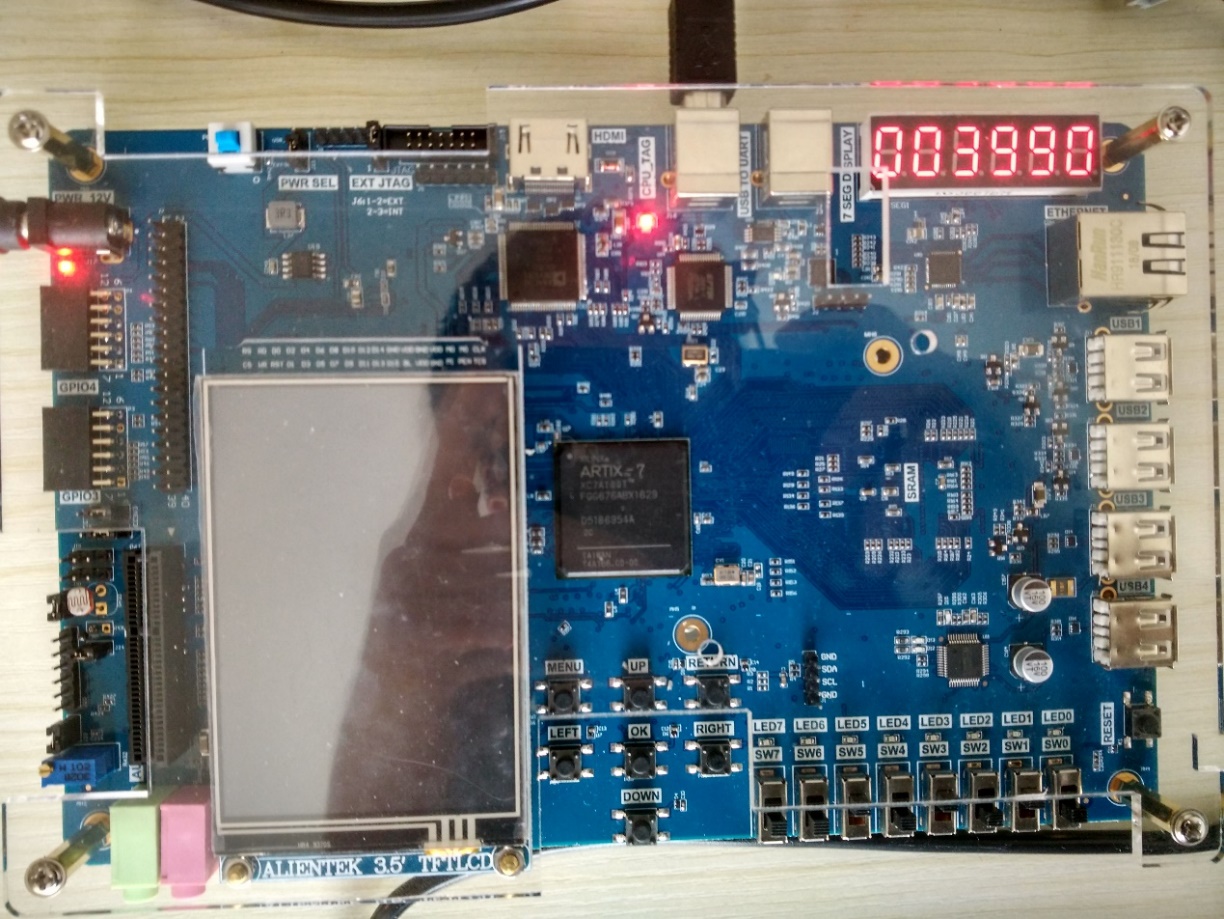
Risc-V Board
Experimental Manuals FPGA Tutor PRX100 Risc-V

Xilinx Risc-V Board Tutorial : Hexadecimal Number to BCD Code Conversion and Application – FII-PRX100 FPGA Board Experiment 8

Experiment 8 Hexadecimal Number to BCD Code Conversion and Application 1.Experiment Objective Since the hexadecimal display is not intuitive, decimal display is more widely used in real life. Human eye recognition is relatively slow, so the display from hexadecimal to decimal does not need to be too fast. Generally, there are two methods Countdown method: Under the control of the synchronous clock, the hexadecimal number is decremented by 1 until it is reduced to 0. At the same time, the appropriate BCD code decimal counter is designed to increment. When…

Read More
Risc-V Board Multiplier Use and ISIM Simulation
Experimental Manuals FPGA Tutor PRX100 Risc-V

Xilinx Risc-V Board Tutorial : Multiplier Use and ISIM Simulation- FII-PRX100 FPGA Board Experiment 7

Experiment 7 Multiplier Use and ISIM Simulation 1.Experiment Objective Learn to use multiplier Use ISIM to simulate design output 2.Experiment Design Build new project mult_sim Select device XC7A100TFGG676-2 Design requirement 8×8 multiplier, the first input value is an 8-bit switch, and the second input value is the output of an 8-bit counter. Observe the result on Modelsim Observe the result on 6 segment decoders Design procedure Create new file mult_sim.v  Add PLL,set the input clock to be 50 MHz, and the output clock to be 100 MHz Add LPM_MULT IP…

Read More
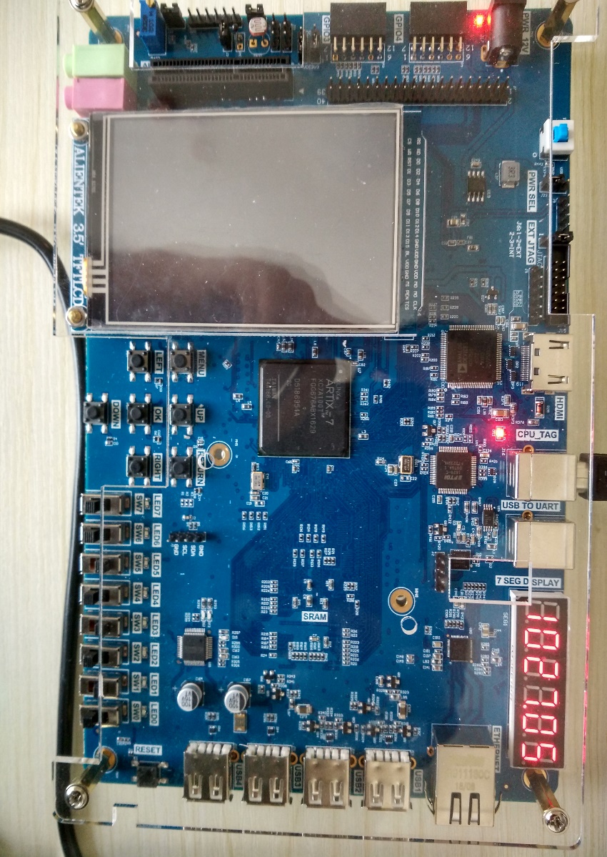
Risc-V Board - Digital Clock Comprehensive Design Experiment
Experimental Manuals FPGA Tutor PRX100 Risc-V

Xilinx Risc-V Board Tutorial : Digital Clock Comprehensive Design Experiment- FII-PRX100 FPGA Board Experiment 6

Experiment 6 Digital Clock Comprehensive Design Experiment 1.Experiment Objective Design month, day, hour, minute, and second digital clock experiments, using 6 segment decoders 60 seconds carried to the minute 60 minutes carried to the hour 24 hours carried to the day 30 days carried to the month, and reset all Set four keys: menu, left, up, down The menu key controls the calibration function to switch between clock, date, and alarm. The left key selects which value is currently calibrated The Up and down keys add 1 and subtract 1…

Read More