FII-PRA040 User Experimental Manuals ( 2020-09-28 Updated )

PRA040 USER EXPERIMENTAL MANUAL
PRA040 EXPERIMENTAL INSTRUCTIONS

FRASER INNOVATION INC
December 07, 2019
Version Control
| Version | Date | Description |
| 1.0 | 07/20/2019 | Initial Release |
| 1.1 | 07/29/2019 | Add Experiment 15 |
| 1.2 | 07/31/2019 | Revised some description about HDMI |
| 1.3 | 08/16/2019 | SRAM part revised |
| 1.4 | 08/30/2019 | Add a description in Ethernet |
| 1.5 | 09/17/2019 | Revise some syntax and code error |
| 1.6 | 12/06/2019 | Add Experiments 16-19 |
Contents
Part One: Introduction of FII-PRA040 Development System 10
1、Design Objective of the System 10
3、Human-computer Interaction Interface 10
4、Software Development System 11
Part Two: FII-PRA040 Main Hardware Resources Usage and FPGA Development Experiment 16
1.4 Experiment Verification 32
1.4.1 Some Preparation Before Verification 32
2.3.1 Introduction of DIP Switches and SignalTap 38
2.4 Use and Verification of SignalTap Logic Analyzer 40
Experiment 3 Segment Display 46
3.3.1 Introduction to the Segment Display 46
3.4 Flash Application and Experimental Verification 54
4.4 Experiment Verification 64
Experiment 5 Button Debounce 65
5.3.1 Introduction to Button and Debounce Principle 65
5.4 Experiment Verification 71
Experiment 6 Use of Multipliers and ModelSim 74
6.3.1 Introduction of Program 74
6.4 Use of ModelSim and the Experiment Verification 78
Experiment 7 Hexadecimal Number to BCD Code Conversion and Application 90
7.2.1 Introduction to the Principle of Converting Hexadecimal Number to BCD Code 90
7.2.2 Introduction of the Program 92
7.4 Application of Hexadecimal Number to BCD Number Conversion 95
7.5 Experiment Verification 97
Experiment Summary and Reflection 99
8.3.1 Introduction of the Program 100
8.4 Experiment Verification 105
Experiment Summary and Reflection 106
Experiment 9 Use Dual-port RAM to Read and Write Frame Data 107
9.3.1 Introduction of the program 108
9.3 Experiment Verification 120
Experiment Summary and Reflection 122
Experiment 10 Asynchronous Serial Port Design and Experiment 124
10.3.1 Introduction to the UART Interface 124
10.3.3 Introduction of the Program 126
10.4 Experiment Verification 133
Experiment 11 IIC Protocol Transmission 135
11.3.1 Introduction of EEPROM and IIC Protocol 135
11.3.2 Hardware Introduction 136
11.3.3 Introduction to the program 137
11.4 Experiment Verification 150
Experiment 12 AD, DA Experiment 153
12.3.1 Introduction to AD Conversion Chip PCF8591 153
Introduction to the Program 155
12.4 Experiment Verification 158
Experiment 13 HDMI Display 162
13.3.1 Introduction to HDMI and ADV7511 Chip 162
13.3.3 Introduction to the Program 164
13.4 Experiment Verification 174
14.3.1 Introduction to Experiment Principle 177
14.3.3 Design of the Program 181
14.4 Experiment Verification 207
Experiment 15 SRAM Read and Write 211
15.3.1 Introduction to SRAM 211
15.3.3 Introduction to the Program 212
15.4 Experiment Verification 219
Experiment 16 8978 Audio Loopback Experiment 225
16.3.1 WM8978 Introduction 225
16.3.2 WM8978 Control Interface Timing 226
16.3.3 I2S Audio Bus Protocol 226
16.3.4 Main Program Design 227
16.4 Experiment Verification 246
Experiment 17 Photo Display Experiment of OV5640 Camera 248
17.4 Experiment Verification 276
Experiment 18 High-speed ADC9226 Acquisition Experiment 282
18.3.1 ADC9226 Module Introduction 282
18.4 Experiment Verification 289
Experiment 19 DAC9767 DDS Signal Source Experiment 292
19.3.2 AD9767 Configuration Introduction 293
19.3.3 Waveform Memory File Configuration 293
19.4 Experiment Verification 302
Project Files Appendix
Experiment 1: LED_shifting
Experiment 2: SW_LED
Experiment 3: BCD_counter
Experiment 4: block_counter
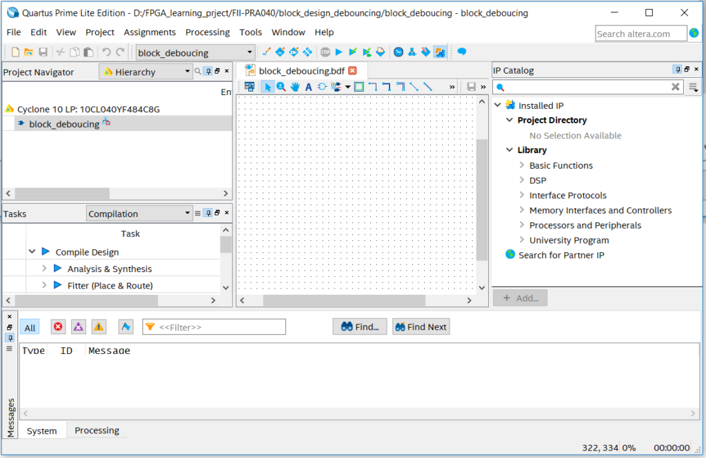
Experiment 5: block_debouncing
Experiment 6: mult_sim
Experiment 7: HEX_BCD,HEX_BCD_mult
Experiment 8: memory_rom
Experiment 9: dual_port_ram
Experiment 10: UART_FRAME
Experiment 11: eeprom_test
Experiment 12: adda_test
Experiment 13: hdmi
Experiment 14: Ethernet
Experiment 15: SRAM
Experiment 16: audio_test
Experiment 17: 5640_camera_pcie
Experiment 18: high_speed_ad
Experiment 19: dac_9767_test
Part One: Introduction of FII-PRA040 Development System
1、Design Objective of the System
The main purpose of this system design is to complete FPGA learning, development and experiment with Intel Quartus. The main device uses the Intel Cyclone10 10CL040YF484C8G and is currently the latest generation of FPGA devices from Intel. The major learning and development projects can be completed as follows:
- Basic FPGA design training
- Construction and training of the SOPC (NiosII) system
- IC design and verification, the system provides hardware design, simulation and verification of RISC-V CPU
- Development and application based on RISC-V
- The system is specifically optimized for hardware design for RISC-V system applications
2、System Resource
- Extended memory: Two Super SRAM (IS61WV25616, 256K x 16bit) are connected in parallel to form a 32-bit data interface, and the maximum access space is up to 1M bytes.
- Serial flash: Spi interface serial flash (16M bytes)
- Serial EEPROM
- Gigabit Ethernet: 100/1000 Mbps
- USB to serial interface: USB-UART bridge
3、Human-computer Interaction Interface
- 8 DIP switches
- 8 push buttons, definition of 7 push buttons: MENU, UP, RETUN, LEFT, OK, RIGHT, DOWN, 1 for reset: RESET
- 8 LEDs
- 6 7-segment LED display
- I2C bus interface
- UART external interface
- Two JTAG programming interfaces: One is for downloading the FPGA debug interface, and the other is the JTAG debug interface for RISC-V CPU
- Built-in RISC-V CPU software debugger, no external RISC-V JTAG emulator required
- 4 12-pin GPIO connectors, in line with PMOD interface standards
4、Software Development System
- Quartus 18.0 and later version for FPGA development, Nios-II SOPC
- Freedom Studio-Win_x86_64 software development for RISC-V CPU
5、Supporting Resources
RISC-V JTAG Debugger
Intel Altera JTAG Download Debugger
FII-PRA040 User Experimental Manual
FII-PRA040 Hardware Reference Guide
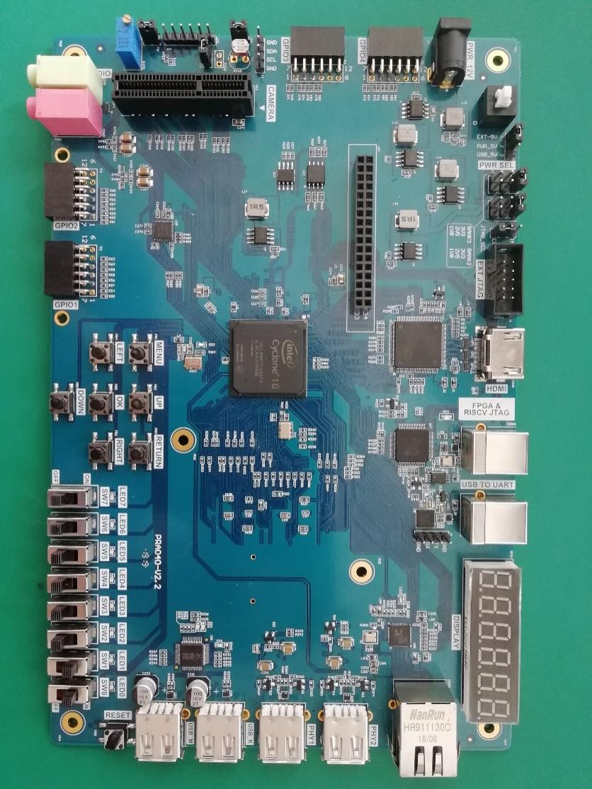
6、Physical Picture
- FII-PRA040 system block diagram
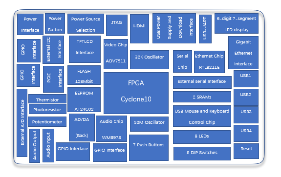
Figure 1 PRA040 system block diagram
- FII-PRA040 physical picture
31
30
29
28
27
26
25
24
23
22
21
20
18
19
17
16
15
14
13
12
11
10
9
8
7
6
5
4
1
3
3
2
Figure 2 PRA040 physical front view
33
32
Figure 3 PRA040 physical back view
- Corresponding to the physical picture, the main devices on board are as follows:
1、10CL040YE484C8G chip
2、External 12V power interface
3、GPIO interface
4、Thermistor (NTC-MF52)
5、Photoresistor
6、Potentiometer
7、Audio output (green), audio input (red)
8、PCIE interface
9、TFTCLD interface
10、Audio chip (WM8978)
11、7 push buttons
12、50M system clock
14、Video chip(ADV7511)
15、External JTAG download interface
16、HDMI interface
17、USB power supply and download interface
18、FPGA and RISC_V JTAG download chips (FT2232)
19、USB_UART interface
20、Serial chip (CP2102)
21、6 7-segment LED display
22、Ethernet interface
23、Ethernet PHY chip (RTL8211E-VB)
24、4 USB interfaces
25、USB mouse and keyboard control chip
26、8 LEDs
27、8-bit DIP switch
28、Reset button
29、Power button
30、Flash (N25Q128A,128M bit/16M bytes)
31、EEPROM (AT24C02N)
32、Two SRAMs
33、AD/DA conversion chip (PCF8591)
Part Two: FII-PRA040 Main Hardware Resources Usage and FPGA Development Experiment
This part mainly guides the user to learn the development of FPGA program and the use of onboard hardware through the development example of FPGA. At the same time, the application system software Quartus is introduced from the elementary to the profound. The development exercises covered in this section are as follows:
Experiment 1: LED shifting design
Experiment 2: SignalTap experiment
Experiment 3: Segment display experiment
Experiment 4: Block/SCH experiment
Experiment 5: button debouncing experiment
Experiment 6: use of multiplier and ModelSim simulation
Experiment 7: hex to BCD conversion and application
Experiment 8: usage of ROM
Experiment 9: use dual-ROM to read and write frame data
Experiment 10: asynchronous serial port design and experiment
Experiment 11: IIC transmission experiment
Experiment 12: AD/DA experiment
Experiment 13: HDMI experiment
Experiment 14: Ethernet experiment
Experiment 15: SRAM read and write
Experiment 16: Audio test
Experiment 17: OV5640 camera experiment
Experiment 18: ADC9226 sampling experiment
Experiment 19: DAC9767 DDS signal source experiment
Learning exercises in the order of the experimental design, and successfully completing these basic experiments, we will be able to achieve the level and capabilities of the primary FPGA engineers.
Experiment 1 LED shifting
1.1 Experiment Objective
- Practice to use Quartus II to create new projects and use system resources IP Core;
- Proficiency in the writing of Verilog HDL programs to develop a good code writing style;
- Master the design of the frequency divider to implement the shifting LED;
- Combine hardware resources to perform FPGA pin assignment and implement actual program downloading;
- Observe the experiment result and summarize it.
1.2 Experiment Implement
- Use all LEDS, all light up during reset;
- End reset, LED lights from low to high (from right to left) in turn;
- Each LED is lit for one second;
- After the last (highest position) LED is lit, the next time it returns to the first (lowest position) LED, the loop is achieved;
1.3 Experiment
1.3.1 LED Introduction
LED (Light-Emitting Diode), is characterized by low operating current, high reliability and long life. Up to now, there are many types of LED lights, as shown in Figure 1.1. The FII-PRA040 uses the LED lights in the red circle.
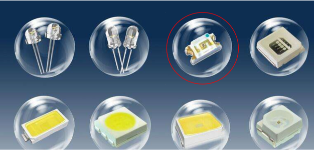
Figure 1.1 Different kinds of LEDs
1.3.2 Hardware Design
The physical picture of the onboard 8-bit LED is shown in Figure 1.2. The schematics of LED is shown in Figure 1.3. The LED module of this experiment board adopts 8 common anode LEDs, which are connected with Vcc 3.3V through 180 R resistors, and the cathodes are directly connected and controlled by the FPGA. When the FPGA outputs a low level of 0, a current flows through the LED, and it is turned on.

Figure 1.2 8-bit LED physical picture
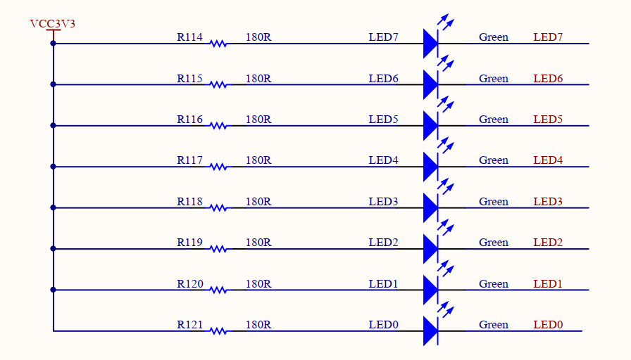
Figure 1.3 Schematics of LED
1.3.3 Program Design
1.3.3.1 Start Program
Before writing a program, let’s briefly introduce the development environment we use and how to create a project. Take Quartus II 18.1 as an example. The specific project establishment steps are shown in Figure 1.4 to 1.9.
- As shown in Figure 1.4, after opening Quartus, you can directly click New Project Wizard in the middle of the screen to create a new project. You can also click File to create a new project in the toolbar, or press Ctrl+N to create a new project.
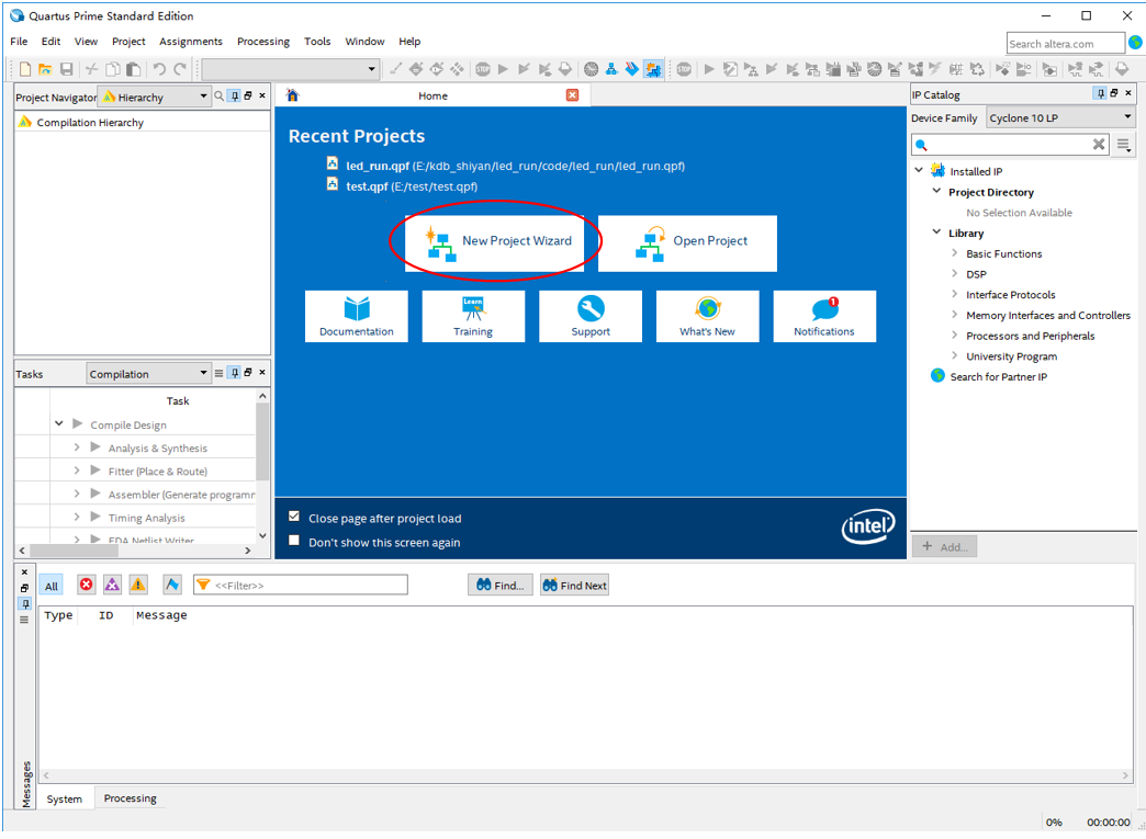
Figure 1.4 The main Quartus II interface
- As shown in Figure 1.5, select the correct project path. The project is named LED_shifting. It is recommended that the path is easy to find and convenient for later viewing and calling.
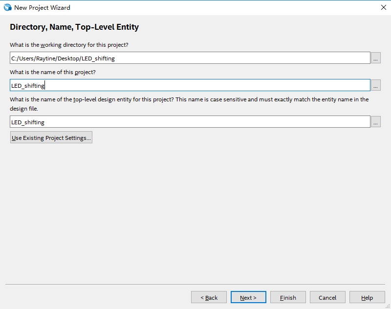
Figure 1.5 Name and define the path of the project file
- As shown in Figure 1.6, you can directly add some files written in advance. Since it is a new project, click Next to perform the next step.
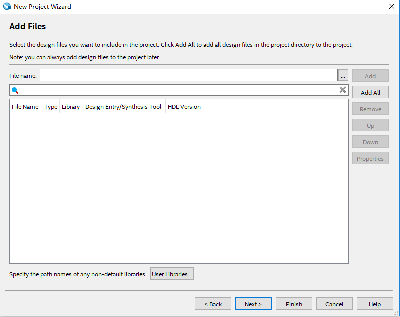
Figure 1.6 Add files
- As shown in Figure 1.7, select the correct FPGA chip model, the onboard chip model is 10CL040YF484C8G. Selecting Cyclone 10 LP in the Family, FBGA in the package, 484 in the Pin count, and 8 in the Core speed grage helps narrow down the selection and quickly find the target model.
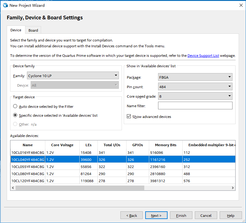
Figure 1.7 Device selection
- As shown in Figure 1.8, select the EDA tool. Here use the EDA tool that comes with Quartus.
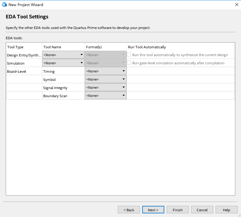
Figure 1.8 Selection of EDA tool
- Click Next to go to the next interface and select Finish to complete the project.
- Click File > New or use the shortcut key Ctrl+N to pop up the dialog box shown in Figure 1.9, create a program file (Verilog HDL File) to write code. Pay attention to the consistency of the program name and project name, and save it in the correct path (folder).
Figure 1.9 Create a new project file (LED_shifting.v)
Once the preparation is ready, start writing the program.
1.3.3.2 Program Introduction
The first step: the establishment of the main program framework (interface design)
|
The input signal of this experiment has 50 MHz system clock clk and reset signal rst_n. Output signal is led; 8 leds are defined by the multi-bit width form of led [7:0].
The second step: the call of IP Core, the establishment and use of PLL module
- As shown in Figure 1.10, find the ALTPLL in the IP catalog option bar on the right side of the main interface.
- As shown in Figure 1.11, double-click ALTPLL and enter the name of the PLL module in the pop-up dialog box. The name given here is PLL1. Note that the selection type is Verilog language type.
- As shown in Figure 1.12, after completing the previous step, enter the detailed setting interface. Inclk0 is the input clock of the PLL, provided by the development board, should be consistent with the system clock, set to 50MHz; PLL feedback path is set to normal mode. For advanced features involved, please read the reference; The output clock of the PLL compensation is C0; after the setting is completed, click Next to proceed to the next step.
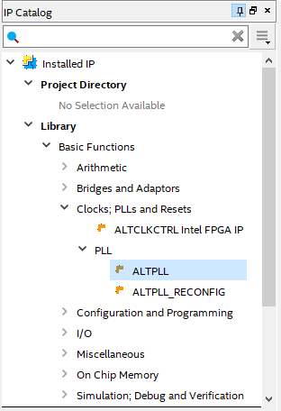
Figure 1.10 IP Catalog
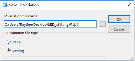
Figure 1.11 Name PLL
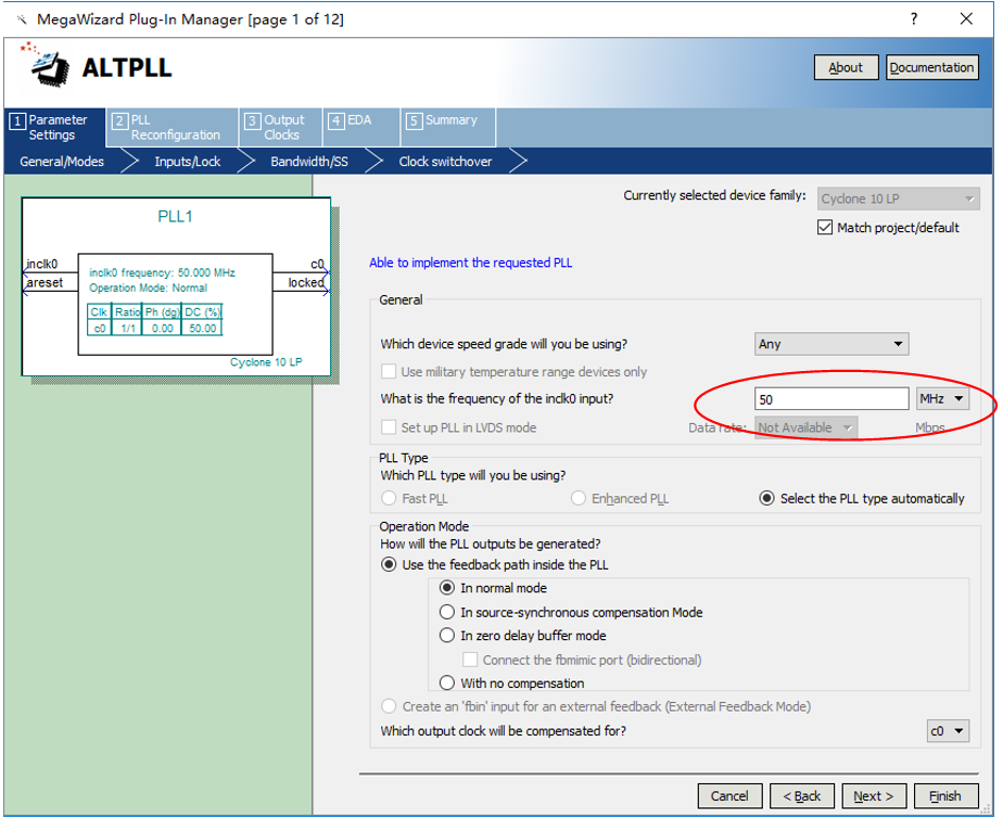
Figure 1.12 PLL setting1 (input clock setting)
- As shown in Figure 1.13, it is the setting of PLL asynchronous reset (areset) control and capture lock (locked) status. This experiment can be selected according to the default mode in the figure.
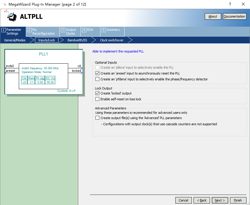
Figure 1.13 PLL setting2
- The contents of the next three settings pages are executed by default.
- As shown in Figure 1.14, it is the setting of the PLL output clock. It can output 5 different clocks clk c0~clk c4. This experiment only uses one, set clk c0, other defaults are not applicable. Set the output frequency to 100 MHz, the clock phase shift to 0, and the clock duty cycle to 50%.
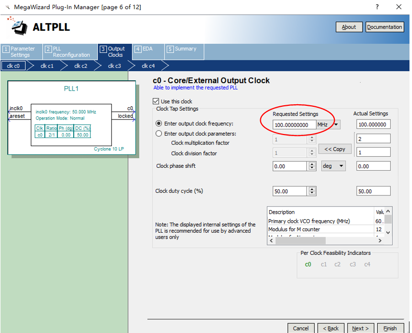
Figure 1.14 PLL setting3 (output clock setting)
- Keep the EDA setting to be default.
- As shown in Figure 1.15, the output file type setting selects *.bsf (used in the subsequent design of graphic symbols) files and *.v files. Others are set by default and click Finish to complete the settings.
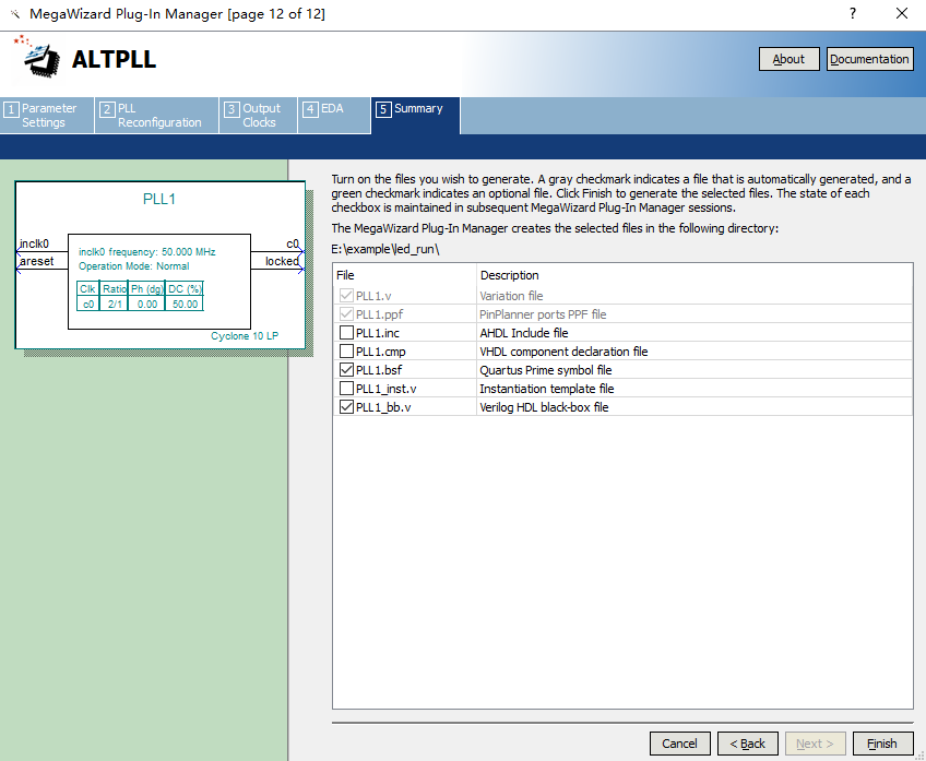
Figure 1.15 PLL settings 4 (Output File Type Settings)
- As shown in Figure 1.16, select file in the Project Navigator type box of the project interface (the default is the project hierarchy).
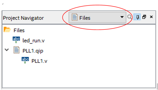
Figure 1.16 PLL1.v file setting
- As shown in Figure 1.17, click PLL1.v. The main window will display the contents of the PLL, find the module name and port list, copy it to the top level entity, and instantiate it.
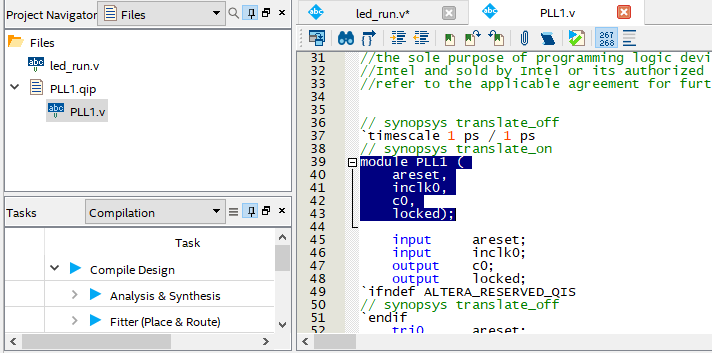
Figure 1.17 PLL1.v file
When the system is powered on, the pll_locked signal has a value of 0 before the PLL is locked (stable operation), pll_locked is pulled high after the PLL is locked, and the clock signal sys_clk is output normally. The phase-locked loop is instantiated as follows:
|
- Sys_rst is used as the reset signal of the frequency division part, and ext_rst is used as the reset signal of the part of the running LED. Under the drive of the clock sys_clk, it is synchronously reset by the primary register.
|
The third step: the design of the frequency divider
We use the 100 MHz clock output by PLL as the system clock. The experiment requires the blinking speed of the running light to be 1 second. The design is firstly obtained 1us by microsecond frequency division, then dividing into milliseconds to get 1ms, and finally get 1s clock through second frequency division.
- Microsecond frequency division
|
The 100 MHz clock has a period of 10ns, and 1us requires 100 clock cycles, that is, 100 10ns. Therefore, a microsecond counter us_cnt [6:0] and a microsecond pulse signal us_f are defined. The counter is cleared at reset. On each rising edge of the clock, the counter is incremented by one. When the counter is equal to 99, the period of 1us elapses, and the microsecond pulse signal us_f is pulled high. Thus, every 1us, this module will generate a pulse signal.
- Millisecond frequency divider
Similarly, 1ms is equal to 1000 1us, so a millisecond counter ms_cnt [9:0] and a microsecond pulse signal ms_f are defined.
|
- Second frequency divider
Similarly, 1s is equal to 1000 1ms, so a second counter s_cnt [9:0] and one second pulse signal s_f are defined. When the three counters are simultaneously full, the time passes for 1 s and the second pulse signal is issued.
|
The fourth step: the design of the shifting LED
When resetting, 8 LEDs are all on, so the output led is 8’h00. The LEDs need to blink one by one, so the lowest LED is lit first. At this time, the led value is 8’b1111_1110. When the second pulse signal arrives, the next LED is illuminated, and the value of led is 8’b1111_1101.It can be seen that as long as the high level of “0” is shifted to the left, it can be realized by bit splicing, that is, led <= {led[6:0], led[7]}.
|
1.4 Experiment Verification
1.4.1 Some Preparation Before Verification
![]()
Synthesis
Pin Assignment
Programmer
Compile
Figure 1.18 Introduction to some functions
As shown in Figure 1.18, after the program is written, analysis and synthesis is required to check for errors. Click the synthesis icon to complete, or use the shortcut key Ctrl+K, the pin assignment is to bind each signal to the FPGA pin, the compilation is to generate the programming file for the development board and check the error again. Click the programmer icon, and follow the instructions to program the development board. Click on the synthesis icon, Quartus will automatically generate a report, as shown in Figure 1.19. The details of the report are not described here.
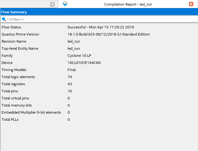
Figure 1.19 Compilation report
Check and modify to no error before board verification. Do the pin assignment before actually programming the board.
Table 1.1 Pin mapping
Click the pin assignment icon to open the pin assignment window, as shown in Figure 1.20. Double-click the location column corresponding to each pin, directly enter the pin number, or click the drop-down button to find the corresponding pin, but the latter is relatively slow. It should be noted that the I/O standard column in Figure 1.21, the content shown is the voltage standard of each I/O port, determined by the BANK voltage in the schematics and the design requirements. In this experiment, the I/O voltage should be selected as 3.3V. Double-click the I/O standard column and click the pull-down button, as shown in Figure 1.22, select the right voltage standard. The default voltage standard can be set in advance when selecting the chip model. Click Device and Pin Options -> Voltage -> Default I/O standard in Figure 1.7 to set it.
The pin assignment is complete, as shown in Figure 1.22. Then click on the compilation. After completion, program the development board.
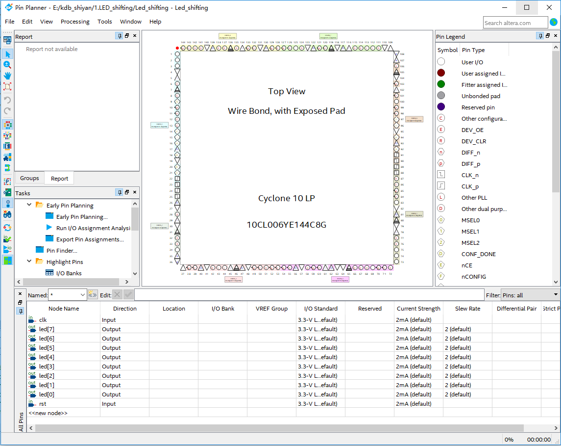
Figure 1.20 Pin assignment window
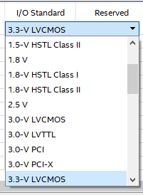
Figure 1.21 I/O voltage selection
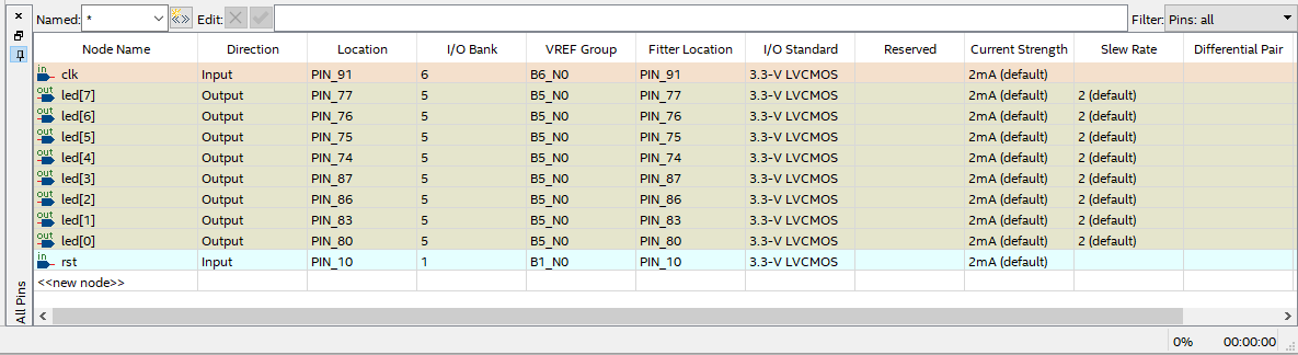
Figure 1.22 Pin assignment overview
1.4.2 Program the Board
Before programming the board, some settings should be made for the Quartus. For details, please refer to the “Intel FPGA Download Cable II User Guide” for reference. After the settings according to the instructions, click programmer icon to open the download window, as shown in Figure 1.23.
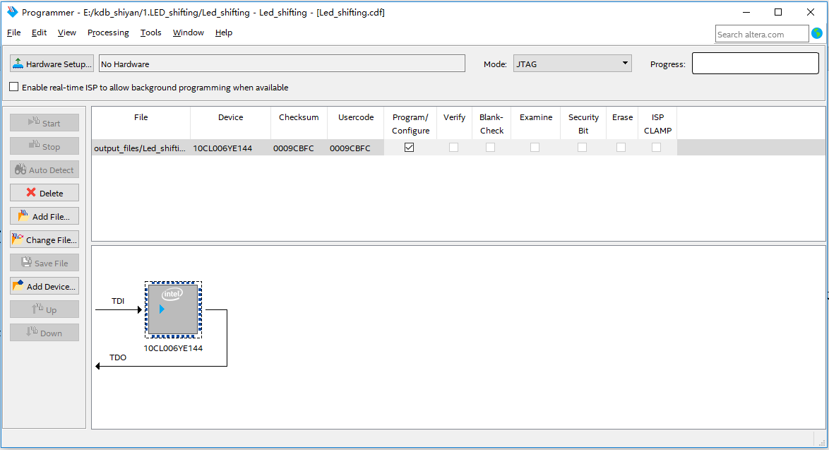
Figure 1.23 Programmer window
After connecting the development board to the host computer, click on Hardware Setup and select development board, as shown in Figure 1.24.
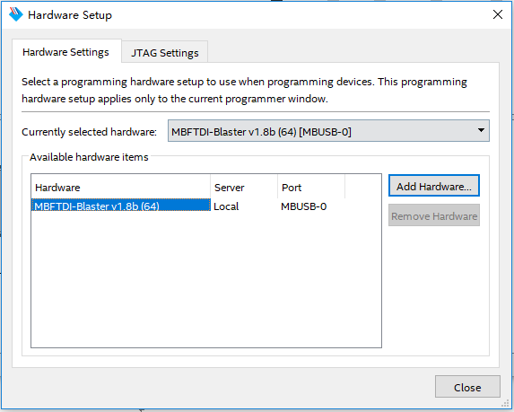
Figure 1.24 Hardwrae setup
Click Start to start the download, as shown in Figure 1.25, Progress shows 100% (Successful), that is, the download is completed.
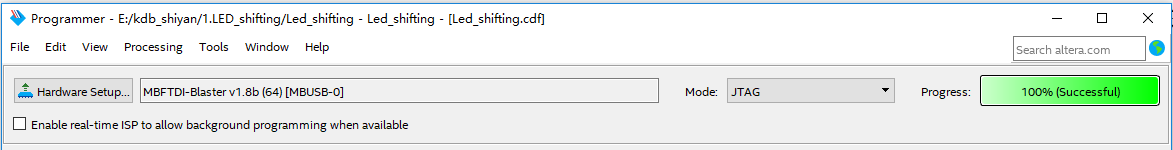
Figure 1.25 Program successfully
See Figure 1.26, the LEDs is lit from low to high and the interval is one second.
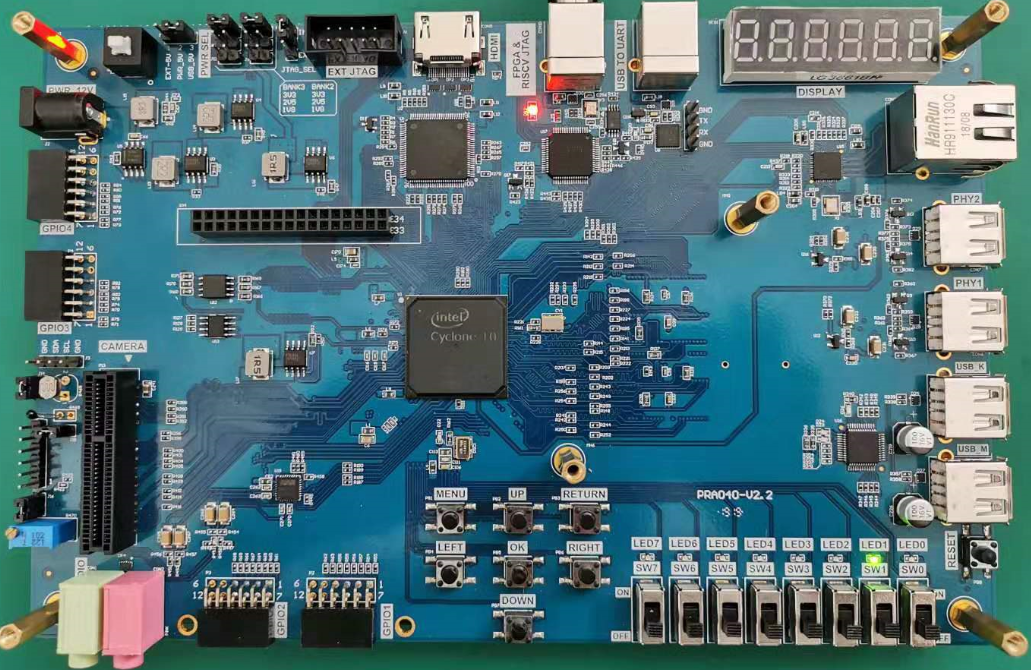
Figure 1.26 Experiment result
Experiment 2 SignalTap
2.1 Experiment Objective
- Continue to practice the use of the development board hardware;
- Practice the use of SignalTap Logic Analyzer in Quartus;
- Learn to analyze the captured signals.
2.2 Experiment Implement
- Use switches to control the LED light on and off
- Capture and analyze the switching signals on the development board through the use of SignalTap.
2.3 Experiment
2.3.1 Introduction of DIP Switches and SignalTap
- Introduction of switches
The on-board switch is 8 DIP switches, as shown in Figure 2.1. The switch is used to switch the circuit by turning the switch handle.
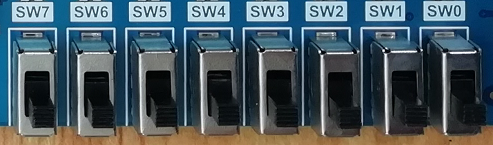
Figure 2.1 Switch physical picture
- Introduction of SignalTap
SignalTap uses embedded logic analyzers to send signal data to SignalTap for real-time analysis of internal node signals and I/O pins when the system is operating normally.
2.3.2 Hardware Design
The schematics of the switch is shown in Figure 2.2. Port 2 of the 8 switches is connected to VCC, and port 3 is connected to the FPGA. Therefore, when the switch is toggled to port 3, the switch is turned on and input to the FPGA a high level signal.

Figure 2.2 Schematics of the switches
2.3.3 Program Design
The first step: the establishment of the main program framework (interface design)
|
The experimental input signals have a system clock clk with frequency of 50 MHz, an high effective 8-bit switch sw, and an output 8-bit led.
The second step: realize the switch control LED
|
When the reset signal is valid, all 8 LEDs are off. After the reset is completed, the LED light is turned on and off by the switch.
2.4 Use and Verification of SignalTap Logic Analyzer
The first step: pin assignment
Pin assignments are shown in Table 2.1. Compile when pin assignment is finished.
Table 2.1 Pin Mapping
| Signal Name | Network Label | FPGA Pin | Port Description |
| clk | C10_50M | G21 | Input clock |
| SW[7] | PB7 | W6 | Switch 7 |
| SW[6] | PB6 | Y8 | Switch 6 |
| SW[5] | PB5 | W8 | Switch 5 |
| SW[4] | PB4 | V9 | Switch 4 |
| SW[3] | PB3 | V10 | Switch 3 |
| SW[2] | PB2 | U10 | Switch 2 |
| SW[1] | PB1 | V11 | Switch 1 |
| SW[0] | PB0 | U11 | Switch 0 |
| led[7] | LED7 | F2 | LED 7 |
| led[6] | LED6 | F1 | LED 6 |
| led[5] | LED5 | G5 | LED 5 |
| led[4] | LED4 | H7 | LED 4 |
| led[3] | LED3 | H6 | LED 3 |
| led[2] | LED2 | H5 | LED 2 |
| led[1] | LED1 | J6 | LED 1 |
| led[0] | LED0 | J5 | LED 0 |
Step 2: SignalTap II startup and basic settings
Menu Tools -> SignalTap II logic Analyzer,
- In Figure 2.3, set the data under Signal Configuration
- Set the JTAG configuration and click on Setup to set the downloader.
- Set the device type by clicking Scan Chain
- Set up SOF Manager: set as *.SOF that is just compiled and generated before
- Clock and storage depth settings are shown in Figure 2.4.
Click the position shown in Figure 2.4 to add the clock. As shown in Figure 2.5, in the Clock Settings dialog box: Filter select SignalTap: pre-synthesis -> List, select the desired clock signal, select c0 in PLL1: PLL1_INST, move to the box on the right.
Other settings can be set as shown in Figure 2.2. (for advanced use of SignalTap II, please read the reference)
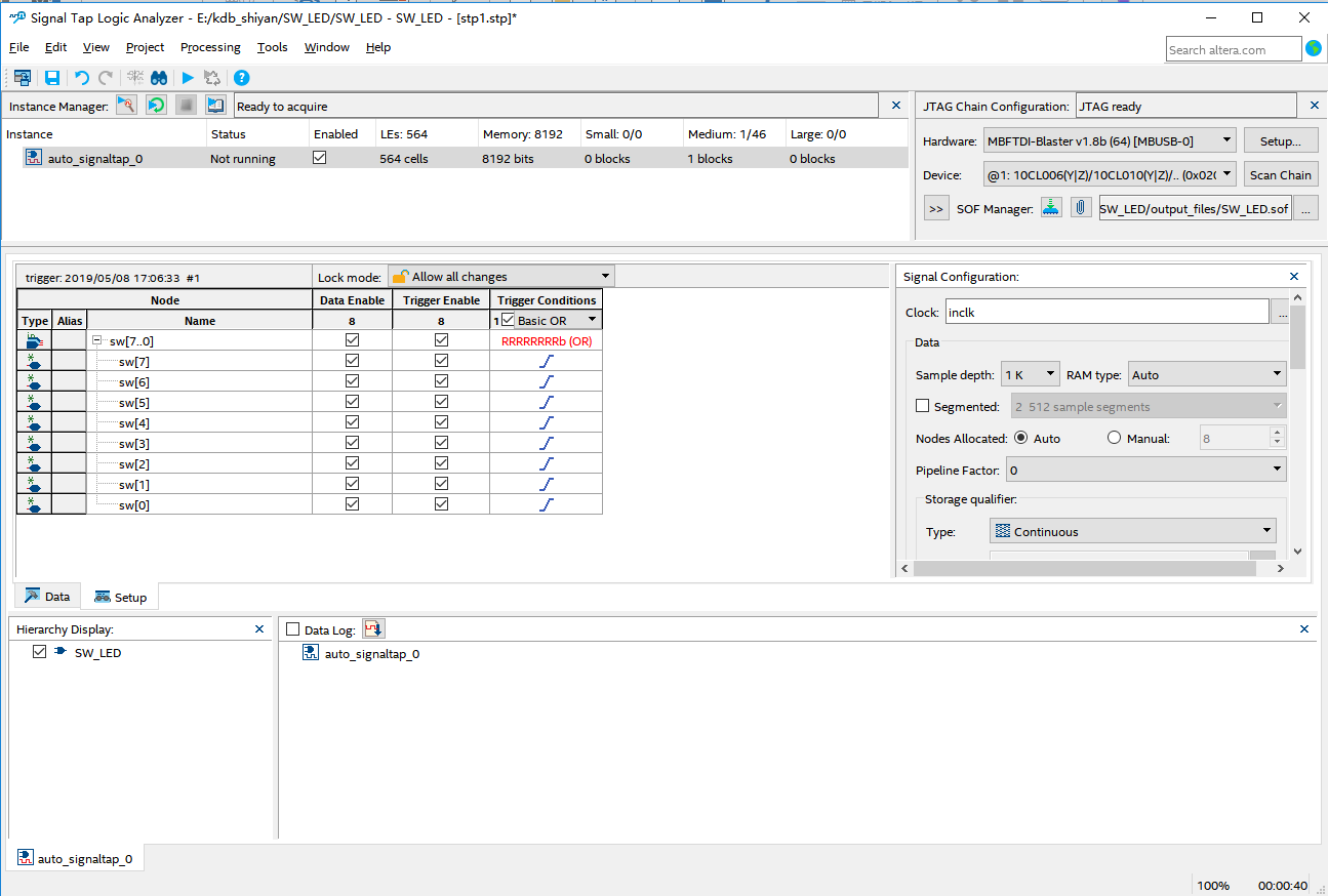
Double click to add nodes
Figure 2.3 SignalTap setting interface
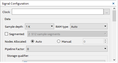
Figure 2.4 Clock signal and the sample depth
Figure 2.5 Clock signal selection dialogue
Step 3: Add observation signal
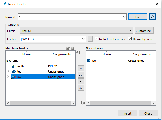
Figure 2.6 Adding interface for the observe signals
As shown in Figure 2.3, double-click the blank to add the observation signal. Adding interface is shown in Figure 2.6. Select the signal you want to observe on the left side, add it to the right side, click Insert. Save it and recompile.
Step 4: Settings of observe signals
For the signal to be observed, whether it is a rising edge trigger, a falling edge trigger, or not care, etc., need to be manually adjusted, as shown in Figure 2.7.
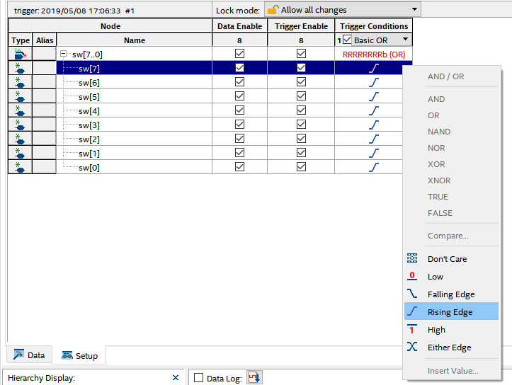
Figure 2.7 Trigger signal setting
Step 5: Observe the results
As shown in Figure 2.7, click Run Analysis to observe the output of SignalTap.
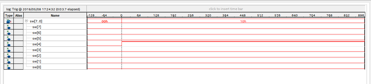
Figure 2.8 Test result
After the switch sw[4] is turned on, its signal is high, and the corresponding LED will be lit. Modify the Trigger condition, test the output results under different Trigger conditions, analyze and summarize.
The experimental phenomenon is shown in Figure 2.9. When the switches sw5 and sw1 are on, the corresponding LED5 and LED1 are illuminated, and the other LEDs remain off.
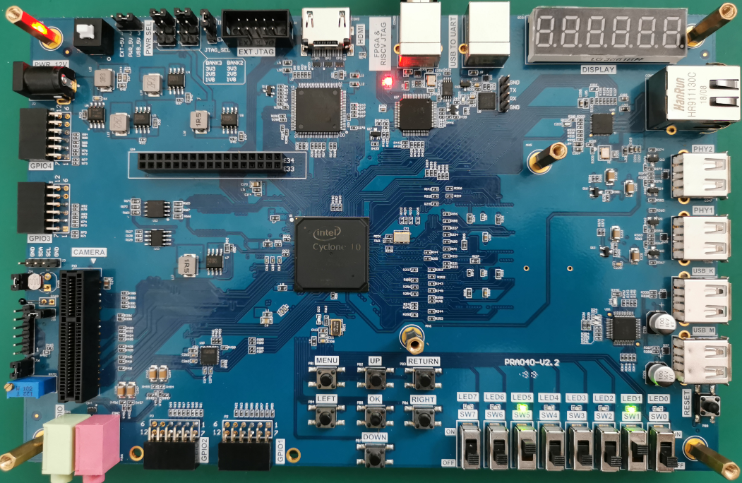
Figure 2.9 Experiment result
Experiment 3 Segment Display
3.1 Experiment Objective
- Review experiment 1, proficient in PLL configuration, frequency division design, and project verification;
- Learn the BCD code counter;
- Digital display decoding design;
- Learn to program the project into the serial FLASH of the development board;
3.2 Experiment Implement
- The segment display has two lower digits to display seconds, the middle two digits to display minutes, and the highest two digits to display hours.
- The decimal point remains off and will not be considered for the time being.
3.3 Experiment
3.3.1 Introduction to the Segment Display
One type of segment display is a semiconductor light-emitting device. The segment display can be divided into a seven-segment display and an eight-segment display. The difference is that the eight-segment display has one more unit for displaying the decimal point, the basic unit is a light-emitting diode. The on-board segment display is a six-in-one eight-segment display as shown in Figure 3.1, and its structure is shown in Figure 3.2.
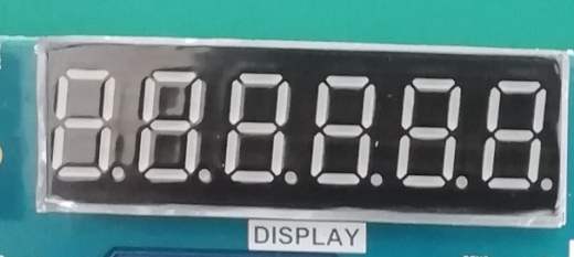
Figure 3.1 Segment display physical picture
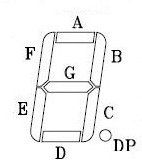
Figure 3.2 Single segment display structure
Common anode segment displays are used here. That is, the anodes of the LEDs are connected. See Figure 3.3. Therefore, the FPGA is required to control the cathode of the LED to be low level, illuminate the diode, and display the corresponding information. The six-digit common anode eight-segment display refers to the signal that controls which one is lit, which is called the bit selection signal. The content displayed by each digital segment is called the segment selection signal. The corresponding truth table is shown in Table 3.1.
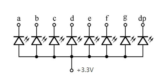
Figure 3.3 Schematics of common anode LEDs
Table 3.1 8-segment display truth table
| Signal Segment | DP | G | F | E | D | C | B | A |
| · | 0 | 1 | 1 | 1 | 1 | 1 | 1 | 1 |
| 0 | 1 | 1 | 0 | 0 | 0 | 0 | 0 | 0 |
| 1 | 1 | 1 | 1 | 1 | 1 | 0 | 0 | 1 |
| 2 | 1 | 0 | 1 | 0 | 0 | 1 | 0 | 0 |
| 3 | 1 | 0 | 1 | 1 | 0 | 0 | 0 | 0 |
| 4 | 1 | 0 | 0 | 1 | 1 | 0 | 0 | 1 |
| 5 | 1 | 0 | 0 | 1 | 0 | 0 | 1 | 0 |
| 6 | 1 | 0 | 0 | 0 | 0 | 0 | 1 | 0 |
| 7 | 1 | 1 | 1 | 1 | 1 | 0 | 0 | 0 |
| 8 | 1 | 0 | 0 | 0 | 0 | 0 | 0 | 0 |
| 9 | 1 | 0 | 0 | 1 | 0 | 0 | 0 | 0 |
| A | 1 | 0 | 0 | 0 | 1 | 0 | 0 | 0 |
| B | 1 | 0 | 0 | 0 | 0 | 0 | 1 | 1 |
| C | 1 | 1 | 0 | 0 | 0 | 1 | 1 | 0 |
| D | 1 | 0 | 1 | 0 | 0 | 0 | 0 | 1 |
| E | 1 | 0 | 0 | 0 | 0 | 1 | 1 | 0 |
| F | 1 | 0 | 0 | 0 | 1 | 1 | 1 | 0 |
There are two ways to display the segment display, static display and dynamic display.
Static display: Each display segment is connected with an 8-bit data line to control and maintain the displayed glyph until the next segment selection signal arrives. The advantage is that the driver is simple, and the disadvantage is that it takes up too much I/O resources.
Dynamic display: Parallel the segment selection lines of all segment display, and the digit selection line controls which digit is valid and lights up. Through the afterglow effect of the LED and the persistence effect of the human eye, the segment display appears to be continuously lit at a certain frequency. The advantage is to save I / O resources, the disadvantage is that the driver is more complicated, the brightness is not static display high.
In this experiment, the digital tube was driven by dynamic scanning.
3.3.2 Hardware Design
The schematics of the segment display is shown in Figure 3.4. The anode is connected to VCC through the P-channel field effect transistor. Therefore, when the bit selection signal SEG_3V3_D[0:5] is low level 0, the FET is turned on, the anode of the segment display is high level; the cathode (segment selection signal) SEG_PA, SEG_PB, SEG_PC, SEG_PD, SEG_PE, SEG_PF, SEG_PG, SEG_DPZ are directly connected to the FPGA and directly controlled by the FPGA. Therefore, when the bit selection signal is 0, and the segment selection signal is also 0, the segment display is lit.
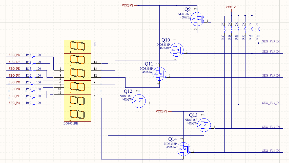
Figure 3.4 Schematics of the segment display
3.3.3 Program Design
3.3.3.1 Introduction of the Program
The first step: the establishment of the main program framework (interface design)
|
The input signal has a clock and a reset signal, and the output signals are a segment selection signal seven_seg and a new signal scan.
Step 2: System Control Module
|
In the first sub-module (system control module), the input clock is the system 50 MHz clock, and a 100MHz is output through the phase-locked loop as the working clock of the other sub-modules. The phase-locked loop lock signal is inverted as the system reset signal. The button is reset to be used as an external hardware reset signal.
The third step: the frequency division module
Referring to Experiment 1, a millisecond pulse signal and a second pulse signal are output as input signals of the segment display driving module.
The fourth step: segment display driver module
- Counting section
The counting part is similar to the frequency dividing module. It is timed by the second pulse signal for 60 seconds, 60 minutes, 24 hours, and when the time reaches 23 hours, 59 minutes and 59 seconds, the counters are all cleared, which is equivalent to one day.
- Segment display dynamic scanning part
|
The dynamic scanning of the segment display is realized by the state machine. A total of six segment display require six states. The state machine scan_state[2:0] is defined, and the corresponding content count_sel is displayed in different states. At reset, all six segment display are extinguished and jump to the 0 state. The segment display is dynamically scanned in 1 millisecond time driven by a millisecond pulse:
In the 0 state, the zeroth segment display is lit, and the ones digit of the second is displayed;
In the 1 state, the first segment display is lit, and the tens digit of the second is displayed;
In the 2 state, the second segment display is lit, and the ones digit of the minute is displayed;
In the 3 state, the third segment display is lit, and the tens digit of the minute is displayed;
In the 4 state, the fourth segment display is lit, and the ones digit of the hour is displayed;
In the 5 state, the fifth segment display is lit, and the tens digit of the hour is displayed;
Part 5: segment display segment code section
|
Referring to Table 3.1, the characters to be displayed are associated with the segment code, the decimal point is set high, and then the final segment selection signal output is composed in a spliced form.
3.4 Flash Application and Experimental Verification
The first step: pin assignment
Pin assignments are shown in Table 3.2.
Table 3.2 Segment display pin mapping
| Signal Name | Network Label | FPGA Pin | Port Description |
| clk | CLK_50M | G21 | Input clock |
| rst_n | PB3 | Y6 | reset |
| scan[0] | SEG_3V3_D0 | F14 | Bit selection 0 |
| scan[1] | SEG_3V3_D1 | D19 | Bit selection 1 |
| scan[2] | SEG_3V3_D2 | E15 | Bit selection 2 |
| scan[3] | SEG_3V3_D2 | E13 | Bit selection 3 |
| scan[4] | SEG_3V3_D4 | F11 | Bit selection 4 |
| scan[5] | SEG_3V3_D5 | E12 | Bit selection 5 |
| seven_seg[0] | SEG_PA | B15 | Segment a |
| seven_seg[1] | SEG_PB | E14 | Segment b |
| seven_seg[2] | SEG_PC | D15 | Segment c |
| seven_seg[3] | SEG_PD | C15 | Segment d |
| seven_seg[4] | SEG_PE | F13 | Segment e |
| seven_seg[5] | SEG_PF | E11 | Segment f |
| seven_seg[6] | SEG_PG | B16 | Segment g |
| seven_seg[7] | SEG_DP | A16 | Segment h |
The second step: compilation
The third step: solidify the program to Flash
Onboard Flash (N25Q128A) is a serial Flash chip that can store 128Mbit of content, which is more than enough for the engineering process in the learning process. The schematics of the Flash is shown in Figure 3.7.
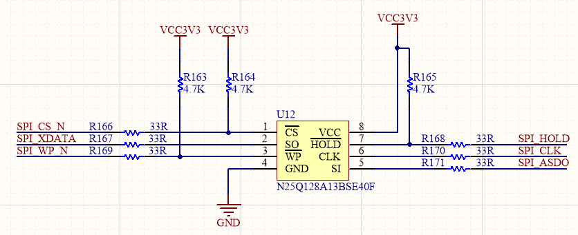
Figure 3.7 Schematics of FLASH
The function of Flash is to save the program on the development board. After the power is off, the program will not disappear. The next time the development board is powered on, it can be used directly. It is more practical in the actual learning life. Driven by the SPI_CLK clock, the FPGA Flash is programmed through the SPI_ASDO line. After power-on, the FPGA re-reads the program to the FPGA through SPI_XDATA for testing.
The specific configuration process of Flash is as follows:
- Menu File -> Convert programming files, as shown in Figure 3.8;
- Option settings
- Select JTAG Indirect configuration File(*.Jic)
- Configuration Device: EPCQ 128A (Compatible with development board N25Q128A)
- Mode: Active serial
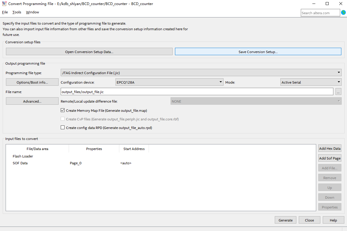
Figure 3.8 *.jic file setting
- Click the Advanced button and set it as shown in Figure 3.9.
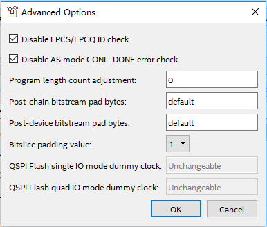
Figure 3.9 Advanced option setting
- Add a conversion file, as shown in Figure 3.10.
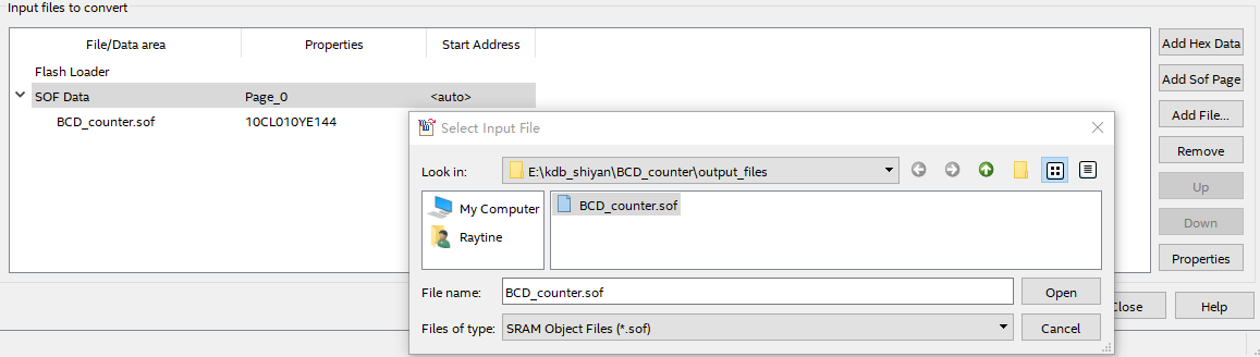
Figure 3.10 Add conversion file
- Add a device, as shown in Figure 3.11.
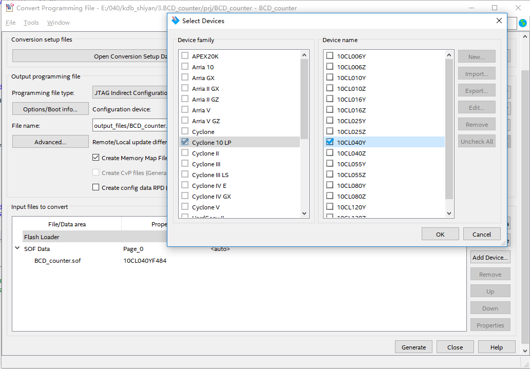
Figure 3.11 Add devices
- Click Generate to generate the BCD_counter.jic file
- Consistent with previous program verification operations, select the correct file (*.jic) to program the development board
The fourth step: power up verification
As shown in Figure 3.12, after repowered on, the FPGA automatically reads the program in Flash into the FPGA and runs it.
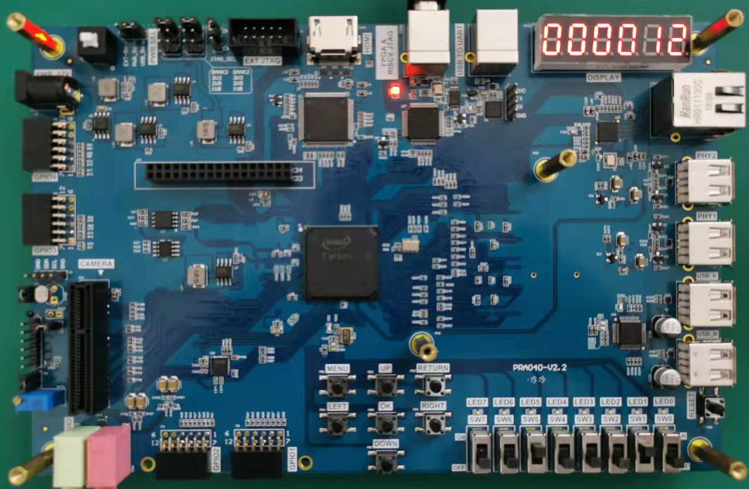
Figure 3.12 Experiment result
Experiment 4 Block/SCH
4.1 Experiment Objective
- Review building new FPGA projects in Quartus, device selection, PLL creation, PLL frequency setting, Verilog’s tree hierarchy design, and the use of SignalTap II
- Master the design method of graphics from top to bottom
- Combined with the BCD_counter project to achieve the display of the digital clock
- Observe the experimental results
4.2 Experiment Implement
Use schematics design to build the project.
4.3 Experiment
This experiment is mainly to master another design method. The other design contents are basically the same as the experiment 3 and will not be introduced in detail. The modular design method is introduced below.
- New project: File -> New Project Wizard…
Project name: block_counter
Select device (10CL040YF484C8G)
- Create new file; File -> New, select Block Diagram/Schematic File. See Figure 4.1.
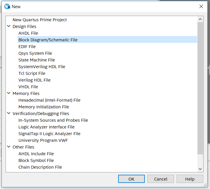
Figure 4.1 New file
- See Figure 4.2, the middle part is the graphic design area, which can be used for Block/SCH design.
- Save the file as block_counter.bdf
- Double-click the blank space in the graphic design area to add a symbol
Figure 4.2 Graph design interface
- Graphic editing
Double-click on the graphic design area to select the appropriate library and device in the libraries
Click to modify the pin name
Figure 4.3 Input symbol
- Add input, output, and modify their names
- Add a custom symbol
- Create a new block/sch file and save it as PLL_sys.bdf
- Add PLL IP, refer to experiment 1
- Select the generated file to include the PLL1.bsf file
- Double-click in the blank area of the PLL_sys.bdf file to select the PLL1 symbol just generated and add it to the file, as shown in Figure 4.4.
Figure 4.4 Invoke the symbols generated in the IP catalog in the graphical editing interface
- Continue to add other symbols, input, output, dff, GND, etc. and connect them, as shown in Figure 4.5.
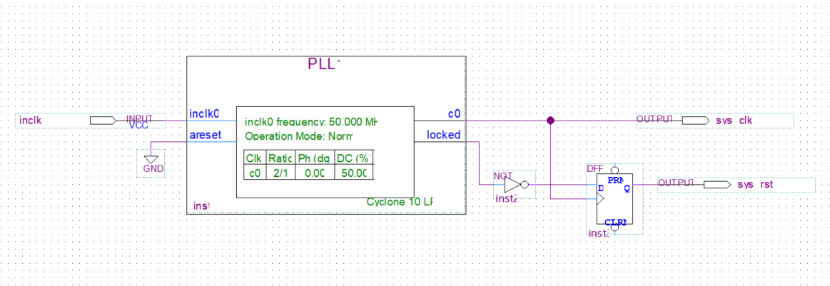
Figure 4.5 Connect the device
- Recreate the newly created file symbol for graphic editing to use in subsequent design
- File -> Create/Update -> Create Symbol file for Current File. See Figure 4.6.
- Generate PLL_sys.bsf
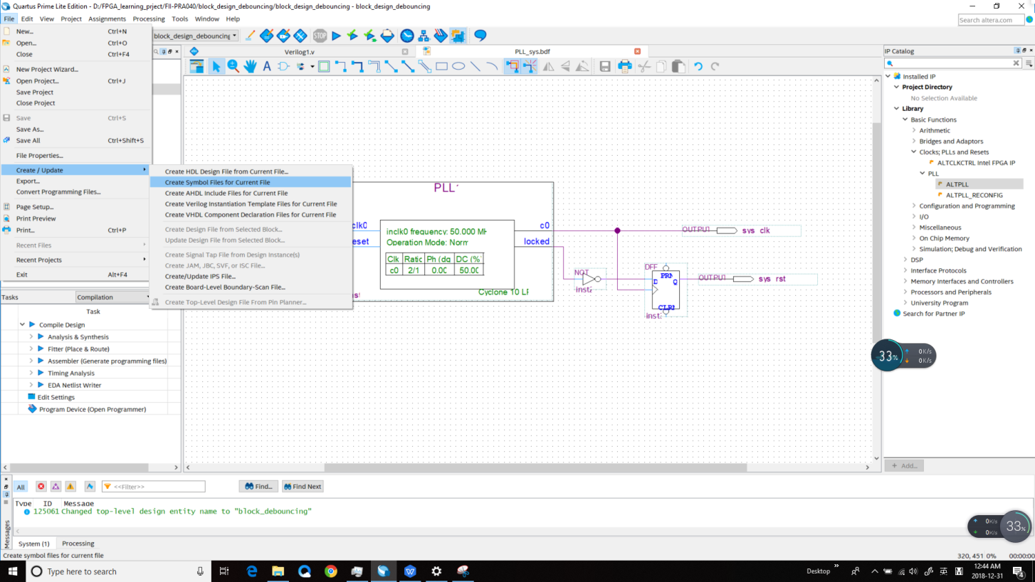
Figure 4.6 Creating a symbol file for the current file (symbol file *.bsf)
- Create a frequency division module
- Create a new verilog file div_us for the frequency divider (Refer project files for the code)
- The PLL output clock is used as its own input clock, and the 100 MHz clock is divided into 1 MHz clocks.
- Repeat (7) to create div_us.bsf
- Create a new 1000 frequency division verilog file: div_1000f.v
- Create div_1000f.bsf symbol
- Create the output pulse us, ms, second module, as shown in Figure 4.7. Refer the specific implementation to the reference code and the frequency division design of the experiment 1 and 3
- Create a new block/sch file block_div and add the designed graphic symbol file to block_div.bdf
- Repeat (7) to create the block_div.bsf symbol
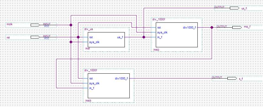
Figure 4.7 us, ms, second pulse of block/sch design
- Create a new verilog file bcd_counter.v, design the hour and minute counter, and create the bsf symbol. Refer to previous experiments and implement part of the frequency division using block_div in (9).
- Combine each *.bsf and complete the design of the digital clock (block_counter.bdf), as shown in Figure 4.8.
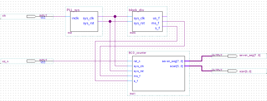
Figure 4.8 Digital clock for BDF design
4.4 Experiment Verification
Pin assignment, compilation, and program verification are consistent with Experiment 3. For reference, see Experiment 3, which is skipped here.
Experiment 5 Button Debounce
5.1 Experiment Objective
- Review the design process of the shifting LED
- Learn button debounce principle and adaptive programming
- Study the connection and use of the Fii-PRA040 button hardware circuit
- Comprehensive application button debounce and other conforming programming
5.2 Experiment Implement
- Control the movement of the lit LED by pressing the button
- Each time the button is pressed, the lit LED moves one bit.
- When the left shift button is pressed, the lit LED moves to the left, presses the right button, and the lit LED moves to the right.
5.3 Experiment
5.3.1 Introduction to Button and Debounce Principle
- Introduction to button
The on-board button are common push buttons, which are valid when pressed, and automatically pops up when released. A total of eight, respectively, PB1 (MENU), PB2 (UP), PB3 (RETURN), PB4 (LEFT), PB5 (OK), PB6 (RIGHT), PB7 (DOWN) and a hardware reset button (RESET). As shown in Figure 5.1.
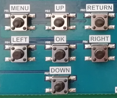
Figure 5.1 Button physical picture
- Introduction to button debounce
As long as mechanical buttons are used, instability should be considered. Usually, the switches used for the buttons are mechanical elastic switches. When the mechanical contacts are opened and closed, due to the elastic action of the mechanical contacts, a push button switch does not immediately turn on when closed, nor is it off when disconnected. Instead, there is some bouncing when connecting and disconnecting. See Fig 5. 2.
The length of the button’s stable closing time is determined by the operator. It usually takes more than 100ms. If pressing it quickly, it will reach 40-50ms. It is difficult to make it even shorter. The bouncing time is determined by the mechanical characteristics of the button. It is usually between a few milliseconds and tens of milliseconds. To ensure that the program responds to the button’s every on and off, it must be debounced. When the change of the button state is detected, it should not be immediately responding to the action, but waiting for the closure or the disconnection to be stabilized before processing. Button debounce can be divided into hardware debounce and software debounce.
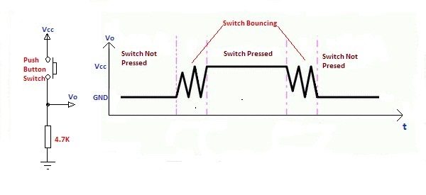
Fig 5. 2 Button bounce principle
In most of cases, software or programs are used to achieve debounce. The simplest debounce principle is to wait for a delay time of about 10ms after detecting the change of the button state, and then perform the button state detection again after the bounce disappears. If the state is the same as the previous state just detected, the button can be confirmed. The action has been stabilized. This type of detection is widely used in traditional software design. However, as the number of button usage increases, or the buttons of different qualities will react differently. If the delay is too short, the bounce cannot be filtered out. When the delay is too long, it affects the sensitivity of the button.
5.3.2 Hardware Design
The schematics is shown in Figure 5.3. One side of the button (P1, P2) is connected to GND, and the other side (P3, P4) is connected to the FPGA. At the same time, VCC is connected through a 10 kohm resistor. In the normal state, the button is left floating, thus the potential of the button P3 is 1, so the input value of the button to the FPGA is 1; when the button is pressed, the buttons are turned on both sides, and the potential of the button P3 is 0, so the input value of the button to the FPGA is 0. The onboard switch is active low.
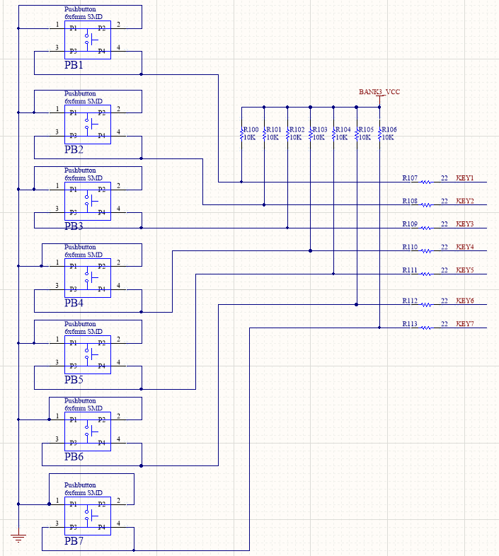
Figure 5.3 Schematics of the buttons
5.3.3 Program Design
5.3.3.1 Top Level Design
See Figure 5. 4.
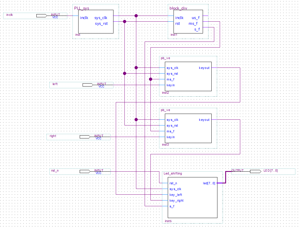
Figure 5.4 Top level design
5.3.3.2 Introduction to the program
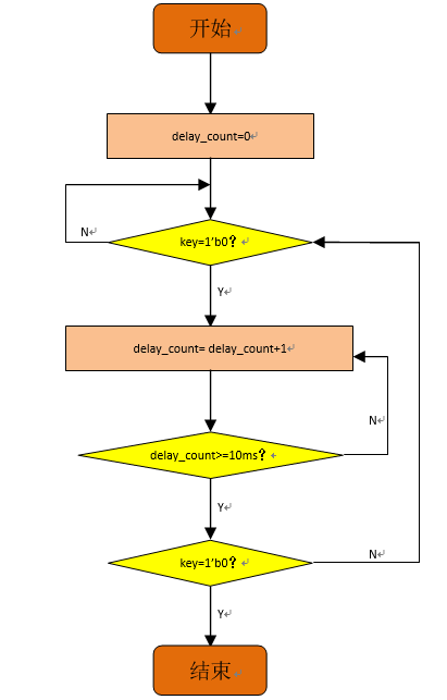
Refer to the previous experiments for the frequency division module and the LED display module. Here, a new part of the button debounce module is introduced. This chapter introduces an adaptive button debounce method: starts timing when a change in the state of the button is detected. If the state changes within 10ms, the button bouncing exists. It returns to the initial state, clears the delay counter, and re-detects the button state until the delay counter counts to 10ms. The same debounce method is used for pressing and releasing the button. The flow chart is shown in Fig 5. 5.Case 0 and 1 debounce the button press state. Case 2 and 3 debounce the button release state. After finishing the whole debounce procedure, the program outputs a synchronized clock pulse.
|
End
Start
Figure 5.5 Button debounce flow chart
5.4 Experiment Verification
The first step: pin assignment
Table 5.1 Pin mapping
| Signal Name | Network Label | FPGA Pin | Port Description |
| left | PB44 | AB4 | Left shift signal |
| right | PB6 | AA4 | Right shift signal |
| clk | CLK_50M | G21 | Input clock |
| rst_n | PB3 | Y6 | Reset |
| led[7] | LED7 | F2 | LED 7 |
| led[6] | LED6 | F1 | LED 6 |
| led[5] | LED5 | G5 | LED 5 |
| led[4] | LED4 | H7 | LED 4 |
| led[3] | LED3 | H6 | LED 3 |
| led[2] | LED2 | H5 | LED 2 |
| led[1] | LED1 | J6 | LED 1 |
| led[0] | LED0 | J5 | LED 0 |
The second step: program the development board
After the pin assignment is completed, the compilation is performed, and the programmer is verified after passing. The experimental phenomenon is shown in Figures below.
All LEDs are lit after successfully programmed. See Figure 5.6.
Figure 5.6 Experiment result (reset)
When the right shift button is pressed, the highest LED lights up. See Figure 5.7.
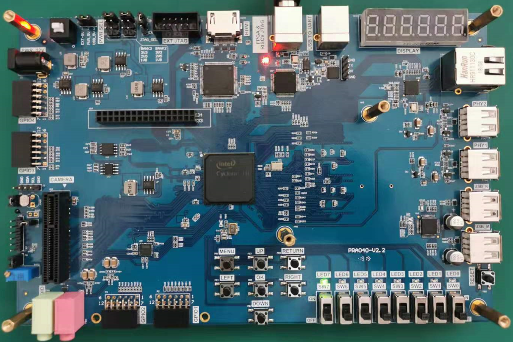
Figure 5.7 Experiment result (one right shift)
Press the right shift button again and the LED will move one bit to the right. See Figure 5.8.
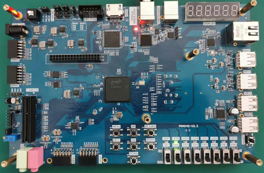
Figure 5.8 Experiment result (another right shift)
Experiment 6 Use of Multipliers and ModelSim
6.1 Experiment Objective
- Learn to use multiplier
- Use ModelSim simulation to design output
6.2 Experiment Implement
- 8×8 multiplier, the first input value is an 8-bit switch, and the second input value is the output of an 8-bit counter.
- Observe the output in ModelSim
- Observe the calculation results with a four-digit segment display
6.3 Experiment
Since the simulation tools and the new IP core are used, there is no introduction or design part of hardware.
6.3.1 Introduction of Program
ModelSim is an HDL language simulation software. Programs can be simulated to achieve inspection and error correction. ModelSim experiment, different from the previous experiment, when building the project, the simulation tool to be used needs to be added in the EDA tool selection window. See Figure 6.1.
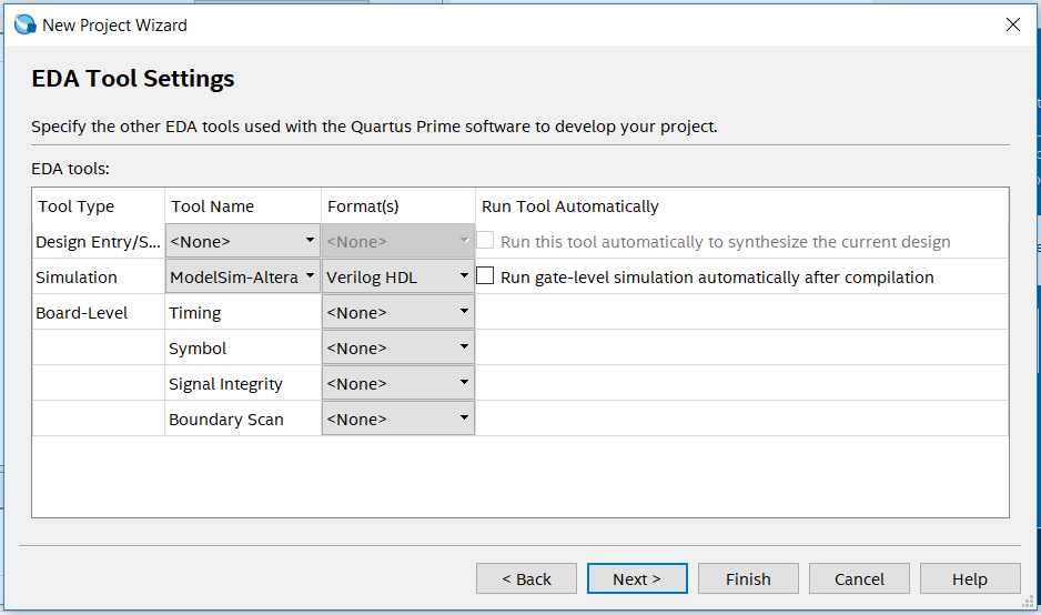
Figure 6.1 EDA tool setting
Only one counter, one PLL and one multiplier are used in the program. Only the multiplier is introduced here.
The first step: the establishment of the main program framework
|
The value of the switch is used as the first input of the multiplier, the value of the counter is the second input, and the result of the calculation is output.
Step 2: the multiplier IP core setting steps are as follows:
After adding the LPM_MULT IP (IP Catalog -> Library -> Basic Functions -> Arithmetic -> LPM_MULT) and saving the path, the setting window of the multiplier is popped up, as shown in Figure 6.2, and the two input data is set to eight bits as required.
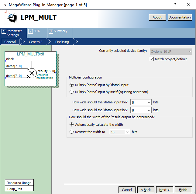
Figure 6.2 mult setting 1
- Select the multiplication type to be Unsigned. See Figure 6.3.

Figure 6.3 mult setting 2
- Select the pipeline to speed up the operation, as shown in Figure 6.4.
- Select others to be default
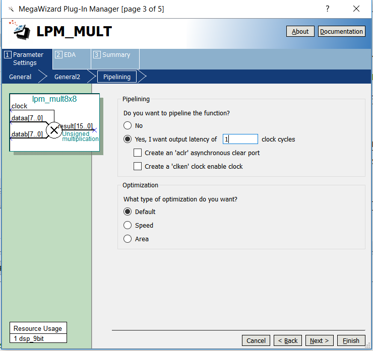
Figure 6.4 mult setting 3
8×8 multiplier instantiation:
|
6.4 Use of ModelSim and the Experiment Verification
Here, use ModelSim to simulate verifying the experiment.
Method 1: Simulation based on waveform input
- Click the menu bar Tools -> Options, as shown in Figure 6.5, click OK.
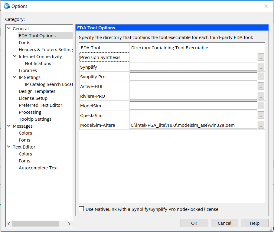
Figure 6.5 Set Modelsim-Altera path
- Tool -> Run Simulation Tool -> RTL Simulation. See Figure 6.6.
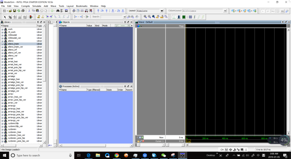
Figure 6.6 ModelSim interface
- Set ModelSim
- Simulate -> Start Simulation
- In the popup window, add libraries under Libraries tag. See Figure 6.7.
Figure 6.7 Add simulation libraries
- Under Design tag, choose simulation project mult_sim and click OK. See Figure 6.8.
Figure 6.8 Choose the project to simulate
- In the Objects window, choose all the signals and drag them to Wave window. See Figure 6.9.
Figure 6.9 Add observation signals
- Set the signals in Wave, right click any signal and a selection window will occur. See Figure 6.10.
Figure 6.10 Set the signals
- Logical signals select Force and select Clock for clock signals
- Set rst signal. See Figure 6.11.
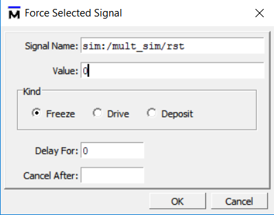
Figure 6.11 Set rst signal
- Set Inclk signal. See Figure 6.12.
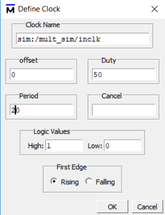
Figure 6.12 Set inclk signal
- Set sw signal. See Figure 6.13.
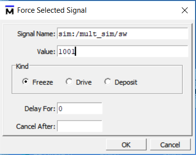
Figure 6.13 Set sw signal
- Run simulation. In the tool bar, set the simulation time to be 100 ns. Click the Run icon to run the simulation. See Figure 6.14.
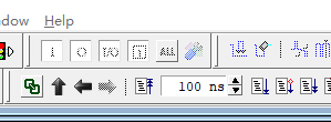
Figure 6.14 Set the simulation time
- Observe the simulation result. See Figure 6.15.
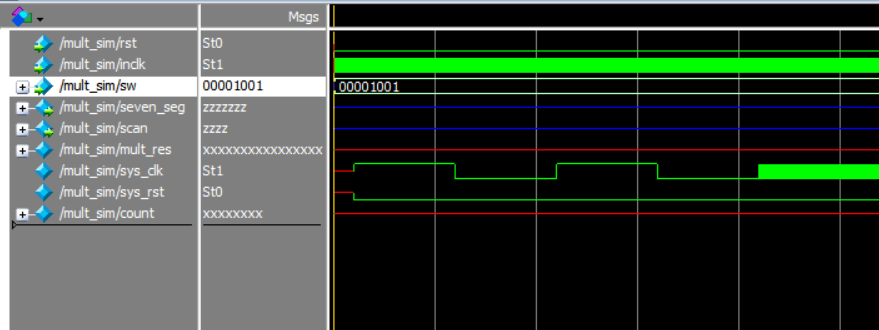
Figure 6.15 Simulation result
- Result analysis
- Counter count does not have a valid result, instead, unknow result XXXXXX is gotten.
- sys_rst does not reset signals. It changes from X to 0
- Add pll_locked signal to the wave, and re-simulate
- In Figure 6.16, before PLL starts to lock, the sys_clk already has a rising edge, so PLL_locked signal is just converted from low to high. There is no reliable reset is formed.
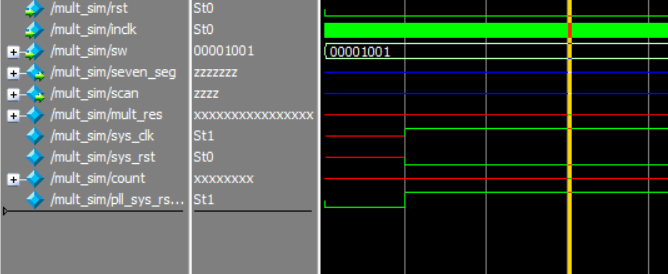
Figure 6.16 Re-simulation result
- Solution
- Define sys_rst to be 1’b1
- Use external rst signal to provide reset
Here method a is adopted. The revised code is as follows:
|
- Recompile the simulation.
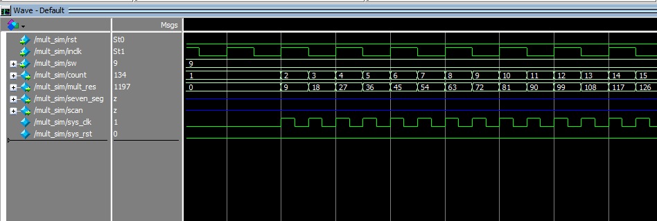
Figure 6.17 Recompile the simulation
Since waveform editing efficiency is relatively low, the use of simulation testbench file is encouraged.
Method 2: Write a testbench file for simulation
- Name a new Verilog HDL file tb_mult.v.
- The code is as follows:
When writing the testbench file, first mark the time unit of the simulation at the beginning, this experiment is 1 ns, then instantiate the project that needs to be simulated into the testbench file, define the clock cycle and the simulation conditions, and stop the simulation after a certain time. This simulation stops after 1000 clock cycles.
After the compilation, the testbench file is added to the ModelSim for simulation, the specific steps are as follows:
- Set the testbench file: Assignments -> Settings. See Figure 6.18.
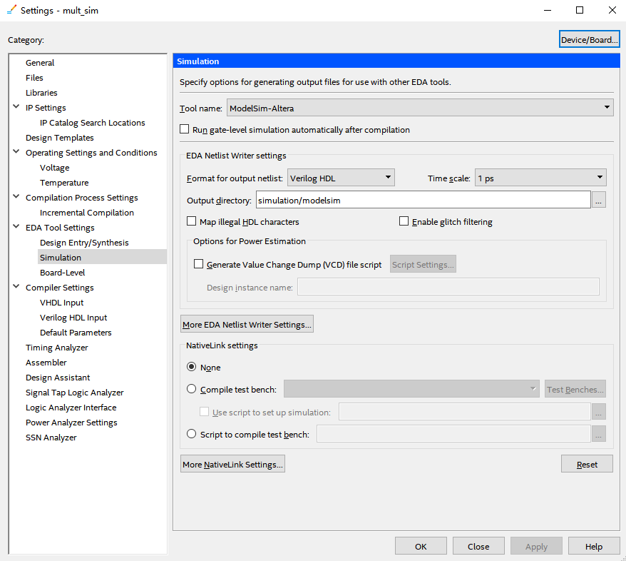
Figure 6.18 Simulation setting 1
- In Compile test bench, click Test Benches to add tb simulation file. See Figure 6.19.
| `timescale 1ns/1ps
module tb_mult; reg rst; reg clk; reg [7:0] sw; wire [7:0] count; wire [15:0] mult_res; // S1 is the instance of simulation module mult_sim S1( .rst (rst), .inclk (clk), .sw (sw), .count (count), .mult_res (mult_res) ); // Define the clock required for the simulation and display the results in text form always begin #10 clk = ~clk; $monitor (“%d * %d = %d”, count, sw, mult_res); end //Set the simulation condition initial begin rst = 0; clk = 1; #10 sw = 20; #10 sw = 50; #10 sw = 100; #10 sw = 101; #10 sw = 102; #10 sw = 103; #10 sw = 104; #50 sw = 105; //stop the signal #1000 $stop; end endmodule |
Figure 6.19 Simulation setting 2
- Click New, input the Test bench name. Make the name be consistent with tb file. See Figure 6. 20.
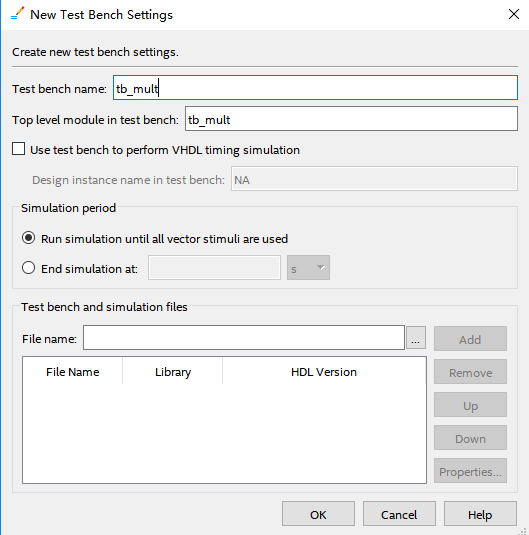
Figure 6.20 Simulation setting 3
- Click the red ellipse to add the test bench file. Find tb_mult.v file written before.
- Click Add to add the file. Click OK (three times) to finish the setting. See Figure 6.21.
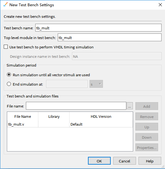
Figure 6.21 Simulation setting 4
- Repeat previous step, to start ModelSim to simulate. See Figure 6.22.
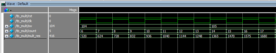
Figure 6.22 Waveform output
After a certain delay, outputs will display in Transcript. See Figure 6.23
Because the result of the operation will be one clock cycle later than the input, the multiplier and the result will differ by one line, which does not seem to match, but does not affect the analysis of the experimental results.

Figure 6.23 Text displays operation result
Summary and Reflection
Try to use the switch as the input to the multiplier. The upper four digits are one number, the lower fourth digits are a number, and the two numbers are multiplied to output the result.
Experiment 7 Hexadecimal Number to BCD Code Conversion and Application
Experiment Objective
- Learn to convert binary numbers to BCD code (bin_to_bcd)
- Learn to convert hexadecimal numbers to BCD code (hex_to_bcd)
7.2 Experimental Implement
Combined with experiment 6, display the results of the operation to the segment display.
7.3 Experiment
7.2.1 Introduction to the Principle of Converting Hexadecimal Number to BCD Code
Since the hexadecimal display is not intuitive, decimal display is more widely used in real life.
Human eyes recognition is relatively slow, so the display from hexadecimal to decimal does not need to be too fast. Generally, there are two methods
- Countdown method:
Under the control of the synchronous clock, the hexadecimal number is decremented by 1 until it is reduced to 0. At the same time, the appropriate BCD code decimal counter is designed to increment. When the hexadecimal number is reduced to 0, the BCD counter Just gets with the same value to display.
- Bitwise operations (specifically, shift bits and plus 3 here). The implementation is as follows:
- Set the maximum decimal value of the expression. Suppose a 16-digit binary value (4-digit hexadecimal) needs to be converted to decimal. The maximum value can be expressed as 65535. First define five four-digit binary units: ten thousand, thousand, hundred, ten, and one to accommodate calculation results
- Shift the hexadecimal number by one to the left, and put the removed part into the defined variable, and judge whether the units of ten thousand, thousand, hundred, ten, and one are greater than or equal to 5, and if so, add the corresponding bit to 3 until the 16-bit shift is completed, and the corresponding result is obtained.
Note: Do not add 3 when moving to the last digit, put the operation result directly
- The principle of hexadecimal number to BCD number conversion
Suppose ABCD is a 4-digit binary number (possibly ones, 10 or 100 bits, etc.), adjusts it to BCD code. Since the entire calculation is implemented in successive shifts, ABCDE is obtained after shifting one bit (E is from low displacement and its value is either 0 or 1). At this time, it should be judged whether the value is greater than or equal to 10. If so, the value is increased by 6 to adjust it to within 10, and the carry is shifted to the upper 4-bit BCD code. Here, the pre-movement adjustment is used to first determine whether ABCD is greater than or equal to 5 (half of 10), and if it is greater than 5, add 3 (half of 6) and then shift.
For example, ABCD = 0110 (decimal 6)
- After shifting it becomes 1100 (12), greater than 1001 (decimal 9)
- By plus 0110 (decimal 6), ABCD = 0010, carry position is 1, the result is expressed as decimal 12
- Use pre-shift adjustment, ABCD = 0110 (6), greater than 5, plus 3
- ABCD = 1001 (9), shift left by one
- ABCD = 0010, the shifted bit is the lowest bit of the high four-bit BCD.
- Since the shifted bit is 1, ABCD = 0010(2), the result is also 12 in decimal.
- The two results are the same
- Firstly, make a judgement, and then add 3 and shift. If there are multiple BCD codes at the same time, then multiple BCD numbers all must first determine whether need to add 2 and then shift.
- The first way is relatively easy. Here, the second method is mainly introduced.
Example 1: Binary to BCD. See Figure 7.1.
Figure 7.1 Example 1, bin_to_bcd
Example 2: Hexadecimal to BCD. See Figure 7.2.
Figure 7.2 hex_to_bcd
7.2.2 Introduction of the Program
The first step: the establishment of the main program framework
|
Enter a 16-bit binary number hex, which can represent a maximum of 65535 decimal, so output ones, tens, hundreds, thousands, and ten_thousands.
The second step: the implementation of bit operation
|
Referring to Figure 7.2, the former part of the program is the judgment calculation part, and if it is greater than or equal to 5, then adds 3. The latter part is the shift part.
Referring to Experiment 6, simulation was performed using ModelSim, and the simulation conditions are set as follows:
|
At the beginning, the 16-bit binary number is equal to 0. The delay is 10 ns. The 16-bit binary number takes a random number less than 20,000. A delay of 10 ns is applied, and the process is repeated 20 times.
After the ModelSim is set and the testbench file is added, perform the simulation. The result is shown in Figure 7.3.
Figure 7.3 Simulation for binary to decimal
Remark and reflection:
- The assignment symbols for the examples above are “=” instead of “<=”. Why?
- Since the whole program is designed to be combinational logic, when invoking the modules, the other modules should be synchronized the timing.
7.4 Application of Hexadecimal Number to BCD Number Conversion
- Continue to complete the multiplier of Experiment 6 and display the result on segment display in decimal. Every 1 second, the calculation results on the segment display changes once. The experiment needs to use frequency division, segment display, multiplier and hexadecimal number to BCD number conversion.
- Compilation. Observe the Timing Analyzer in Compilation Report.
- Fmax Summary 83.71 MHz. See Figure 7.4.
Figure 7.4 Fmax Summary
- Setup Memory
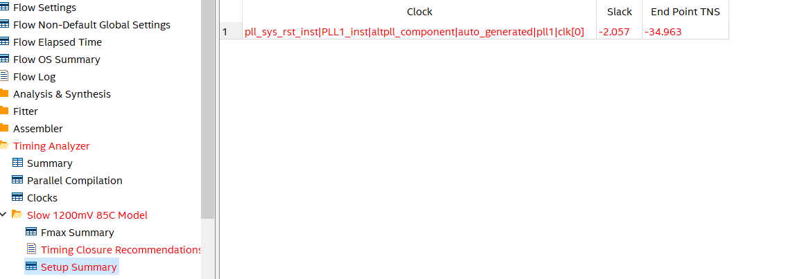
Figure 7.5 Setup time summary
- Timing Closure Recommendation. See Figure 7.6.
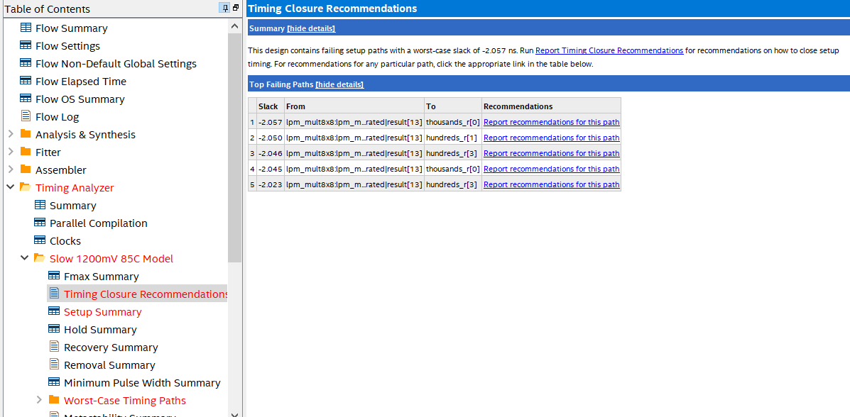
Figure 7.6 Timing Analysis
- From the above three indicators, the above programming does not meet the timing requirements. It can also be seen that the maximum delay path is the delay of the output of the multiplier to HEX_BCD.
There are 3 solutions:
- Reduce the clock frequency
- Increase the timing of HEX_BCD and increase the pipeline
- Insert pipeline isolation at the periphery (can reduce some delay)
The way to increase the pipeline, will be introduced in the follow-up experiment, because the function of HEX_BCD is mainly used to display the human-machine interface, the speed requirement is low, and the frequency reduction method is adopted here.
- Modify PLL to increase an output of 20 MHz frequency (BCD_clk)
- Recompile and observe timing results
- Lock the pins, compile, and program FII-PRA040 development board for testing
7.5 Experiment Verification
The first step: pin assignment
Table 7.1 Hexadecimal number to BCD pin mapping
| Signal Name | Network Label | FPGA Pin | Description |
| clk | CLK_50M | G21 | Input clock |
| rst_n | PB3 | Y6 | Reset |
| scan[0] | SEG_3V3_D5 | F14 | Bit selection 0 |
| scan[1] | SEG_3V3_D4 | D19 | Bit selection 1 |
| scan[2] | SEG_3V3_D3 | E15 | Bit selection 2 |
| scan[3] | SEG_3V3_D2 | E13 | Bit selection 3 |
| scan[4] | SEG_3V3_D1 | F11 | Bit selection 4 |
| scan[5] | SEG_3V3_D0 | E12 | Bit selection 5 |
| seven_seg[0] | SEG_PA | B15 | Segment a |
| seven_seg[1] | SEG_PB | E14 | Segment b |
| seven_seg[2] | SEG_PC | D15 | Segment c |
| seven_seg[3] | SEG_PD | C15 | Segment d |
| seven_seg[4] | SEG_PE | F13 | Segment e |
| seven_seg[5] | SEG_PF | E11 | Segment f |
| seven_seg[6] | SEG_PG | B16 | Segment g |
| seven_seg[7] | SEG_DP | A16 | Segment h |
| SW[7] | PB7 | W6 | Swicth 7 |
| SW[6] | PB6 | Y8 | Swicth 6 |
| SW[5] | PB5 | W8 | Swicth 5 |
| SW[4] | PB4 | V9 | Swicth 4 |
| SW[3] | PB3 | V10 | Swicth 3 |
| SW[2] | PB2 | U10 | Swicth 2 |
| SW[1] | PB1 | V11 | Swicth 1 |
| SW[0] | PB0 | U11 | Swicth 0 |
Step 2: development board verification
After the pin assignment is completed, the compilation is performed. Program the development board for verification after passing. The experimental result is shown in Figure 7.7. The value of the DIP switch input is 00001010, decimal 10, the counter is constantly accumulating, so the display result is always accumulatively changed by 10.
Figure 7.7 Experiment phenomenon
Experiment Summary and Reflection
- How to implement BCD using more than 16 bits binary numbers
- What is a synchronous clock and how to handle an asynchronous clock
- Learn to design circuits meeting the requirement
Experiment 8 Use of ROM
8.1 Experiment Objective
- Study the internal memory block of FPGA
- Study the format of *.mif and how to edit *.mif file to configure the contents of ROM
- Learn to use RAM, read and write RAM
8.2 Experiment Implement
- Design 16 outputs ROM, address ranging 0-255
- Interface 8-bit switch input as ROM’s address
- Segment display the contents of ROM and require conversion of hexadecimal to BCD output.
8.3 Experiment
8.3.1 Introduction of the Program
This experiment was carried out on the basis of Experiment 7, and the contents of Experiment 7 were cited, so only the IP core ROM portion is introduced here.
- In Installed IP, choose Library -> Basic Function -> On Chip Memory -> ROM: 1-PORT, file type to be Verilog HDL. Choose 16 bits and 256 words for output. See Figure 8.1.
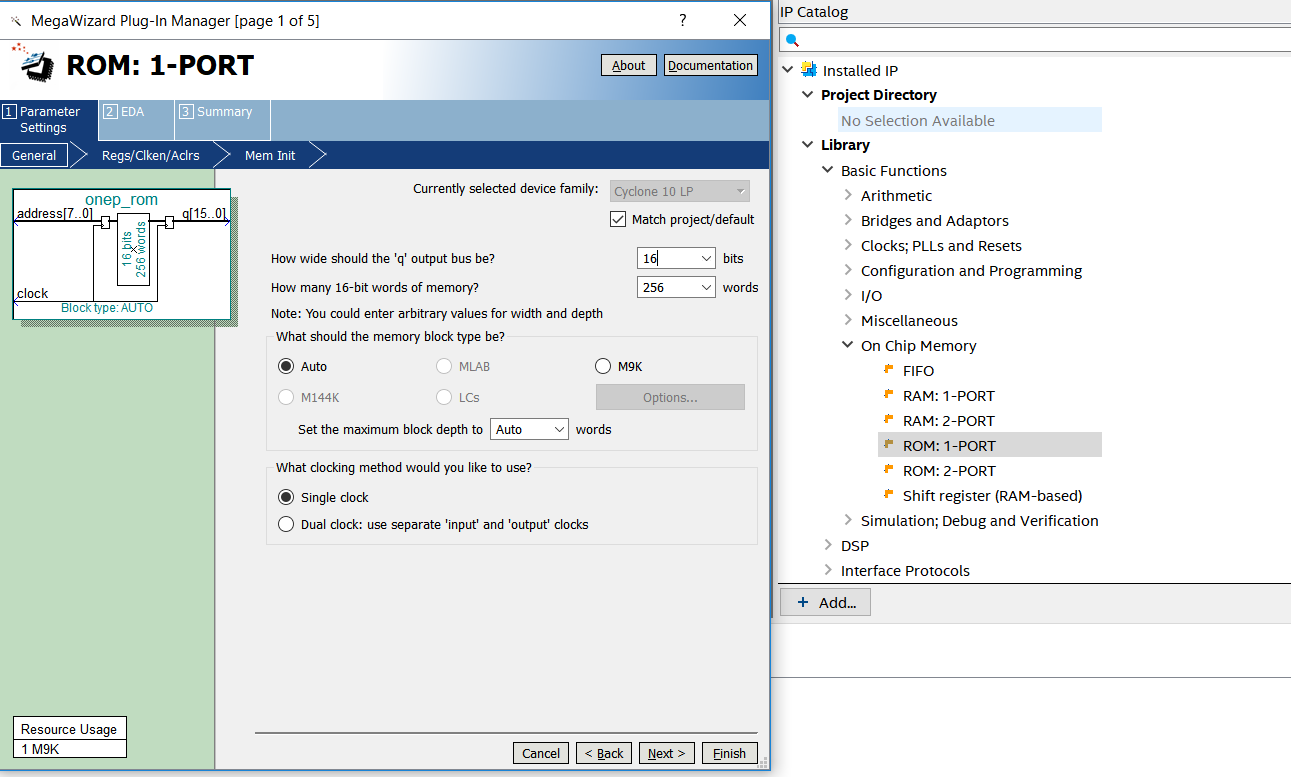
Figure 8.1 RAM IP core invoking
- According to the default setting, an initial ROM file in the location where red oval circles needs to be added. See Figure 8.2. In the figure, a *.mif file has already been added.
- Create a top level entity rom.mif
- Generate rom.mif file. Go to File -> New -> Memory Files -> Memory Initialization File. See Figure 8.3.
- In Figure 8.4, modify the Number of words and Word size.
- In Figure 8.5, in the address area, right click to input the data or change the display format, such as hexadecimal, octal, binary, unsigned, signed, etc.
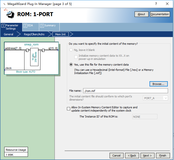
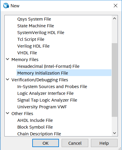
Figure 8.3 New *.mif file
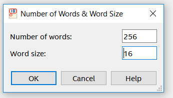
Figure 8.4 *.mif file setting 1
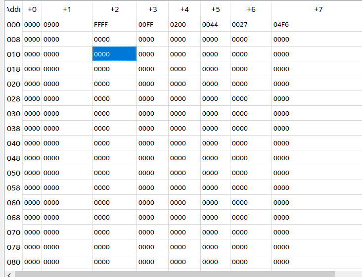
Figure 8.5 *.mif file setting 2
- After completing the ROM and IP’s setting, fill the data for rom.mif. For convenience of verification, store the same data as the address from the lower byte to higher byte in ascending form. Right click to select Custom Fill Cells. See Figure 8.6. The starting address is 0, ending at 255 (previous address setting depth is 256). The initial value is 0 and the step is 1.
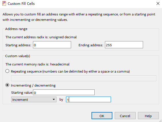
Figure 8.6 Fill date for rom.mif
- After the setup, the system will fill in the data automatically. See Figure 8.7.
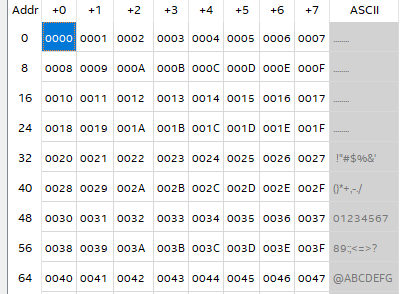
Figure 8.7 Part of data after auto filling
Refer to the design of conversion from hexadecimal to BCD in Experiment 7, display the data in ROM on the segment display.
ROM instantiation:
|
8.4 Experiment Verification
Pin assignments are consistent with Experiment 7. After the compilation is completed, the board is verified. As shown in Figure 8.8. When the DIP switch is 10010100, the decimal expression is 148, which means the contents of the 148th byte of the ROM is read, and the segment display will illustrate 148, which is consistent with the data deposited before.
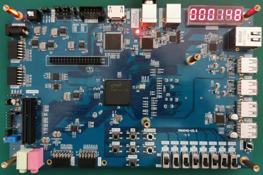
Figure 8.8 Experiment result
Experiment Summary and Reflection
- How to use the initial file of ROM to realize the decode, such as decoding and scanning the segment display.
- Write a *.mif file to generate sine, cosine wave, and other function generators.
- Comprehend application, combine the characteristic of ROM and PWM to form SPWM modulation waveform.
Experiment 9 Use Dual-port RAM to Read and Write Frame Data
9.1 Experiment Objective
- Learn to configure and use dual-port RAM
- Learn to use synchronous clock to control the synchronization of frame structure
- Learn to use asynchronous clock to control the synchronization of frame structure
Experiment Implement
- Observing the synchronization structure of synchronous clock frames using SignalTap II
- Extended the use of dual-port RAM
- Design the use of three-stage state machine
- Design a 16-bit data frame
- Data is generated by an 8-bit counter: Data={~counta,counta}
- The ID of the data frame inputted by the switch (7 bits express maximum of 128 different data frames)
- 16-bit checksum provides data verification
- 16-bit checksum accumulates, discarding the carry bit
- After the checksum is complemented, append to the frame data
- Provide configurable data length data_len by parameter
- Packet: When the data and checksum package are written to the dual-port RAM, the userID, the frame length and the valid flag are written to the specific location of the dual-port RAM. The structure of the memory is shown in Table 9.1.
Table 9.1 Memory structure
| Wr_addr | Data/Flag | Rd_addr |
| 8’hff | {valid,ID,data_len} | 8’hff |
| … | N/A | … |
| 8’hnn+2 | N/A | 8’hnn+2 |
| 8’hnn+1 | ~checksum+1 | 8’hnn+1 |
| 8’hnn | datann | 8’hnn |
| … | …. | … |
| 8’h01 | Data1 | 8’h01 |
| 8’h00 | Data0 | 8’h00 |
- Read and write in an agreed order
Valid is the handshake signal. This flag provides the possibility of read and write synchronization, so the accuracy of this signal must be ensured in the program design.
9.3 Experiment
9.3.1 Introduction of the program
The first step: the establishment of the main program framework
|
The second step: the definition of the state machine
|
The third step: other definitions
|
Step 4: Generate dual-port RAM, PLL
|
The RAM is 16 bits wide and 256 depth. The PLL inputs a 50 MHz clock, outputs 100 MHz as the operating clock of other modules, and 20 MHz is used to drive the segment display.
Step 5: data generation counter
|
Step 6: write state machine
|
| //Third stage
always @ (posedge sys_clk) begin case (sta) mema_idle : begin addr_a <= 8’hff; wren_a <= 1’b0; data_a <= 16’b0; wr_len <= 8’b0; wr_chsum <= 0; end mema_init, mema_pipe0, mema_read0, mema_read1 : begin addr_a <= 8’hff; wren_a <= 1’b0; data_a <= 16’b0; wr_len <= 8’b0; wr_chsum <= 0; end mema_wr_data : begin addr_a <= addr_a + 1’b1; wren_a <= 1’b1; data_a <= {countb, counta}; wr_len <= wr_len + 1’b1; wr_chsum <= wr_chsum + {countb, counta}; end mema_wr_chsum : begin addr_a <= addr_a + 1’b1; wr_len <= wr_len + 1’b1; wren_a <= 1’b1; data_a <= (~wr_chsum) + 1’b1; end mema_wr_done : begin addr_a <= 8’hff; wren_a <= 1’b1; data_a <= {1’b1, user_id, wr_len}; end default : ; endcase end |
Write order:
- Read the flag of the 8’hff address (control word). If valid=1’b0, the program proceeds to the next step, otherwise waits
- Address plus 1, 8’hff+1 is exactly zero, write data from 0 address and calculate the checksum
- Determine whether the predetermined data length is reached. If so, proceeds to next step, otherwise continue writing the data, and the checksum is calculated.
- checksum complements and write to memory
- Write the control word in the address 8’hff, packet it
Step 7: read state machine
|
//Stage three, the actual operation needs to be driven by the edge of the clock.
|
Read order
- idle is the state after reset
- Init: Initialization, set the address to 8’hff
- Rd_pipe0: Add a latency (since the read address and data are both latched). Address +1, forming a pipeline structure
- Read0: Set the address to 8’hff, read the control word and judge whether the valid bit is valid.
- If valid=1’b1, address +1, proceeds to the next step
- If valid=1’b0, it means the packet is not ready yet, the address is set to be 8’hff and returns to the init state.
- Read1: Read the control word again
- If valid=1’b1, address+1, ID and data length are assigned to the corresponding variables and proceeds to the next step
- If valid=1’b0, it means the packet is not ready yet, the address is set to 8’hff, and returns to the init state.
- Rd_data:
- Read data and pass to data variables
- Calculate checksum, data_len – 1
- Determine whether the data_len is 0
- 0: all data has been read, proceeds to the next step
- Not 0: continue the operation in current state
- rd_chsum: Read the value of checksum and calculate the last checksum. Correct the data and set the flag of rd_err
- rd_done: The last step clears the valid flag in memory and opens the write enable for the next packet.
Experiment Verification
The first step: pin assignment
Table 9.2 Frame data read and write experiment pin mapping
| Signal Name | Network Label | FPGA Pin | Port Description |
| Inclk | CLK_50M | G21 | Input clock |
| rst | PB3 | Y6 | reset |
| SW[7] | SW7 | W6 | Switch input 7 |
| SW[6] | SW6 | Y8 | Switch input 6 |
| SW[5] | SW5 | W8 | Switch input 5 |
| SW[4] | SW4 | V9 | Switch input 4 |
| SW[3] | SW3 | V10 | Switch input 3 |
| SW[2] | SW2 | U10 | Switch input 2 |
| SW[1] | SW1 | V11 | Switch input 1 |
| SW[0] | SW0 | U11 | Switch input 0 |
Step 2: Observe the read and write results of the dual-port RAM with SignalTap
- In order to facilitate the observation of the read and write state machine synergy results, the data length is changed to 4 here and recompile. Users can test themselves using long data.
|
- Observe the simulation result
- Observe the handshake mechanism through dual-port RAM
- Determine whether the reading is started after the packet is written
- Determine whether the write packet is blocked before reading the entire packet is completed
- Observe the external interface signal and status
- rd_done, rd_err
Set rd_err = 1, or the rising edge is the trigger signal to observe whether the error signal is captured
- Observe whether wren_a, wren_b signal and the state machine jump are strictly matched to meet the design requirements
- SignalTap result. See Figure 9.1.
Experiment Summary and Reflection
- Review the design requirements of how to analyze an actual demand, to gradually establish a model of digital control and state machine and finally design it.
- Modify the third stage of the state machine into the if…else model and implement.
- Focus on thinking If the read and write clocks are different. After it becomes an asynchronous mechanism, how to control the handshake protocol.
- According to the above example, consider how dual-port RAM can be used in data acquisition, asynchronous communication, embedded CPU interface, and DSP chip interface.
- How to build ITCM with dual-port RAM and DTCM preparing for future CPU design.
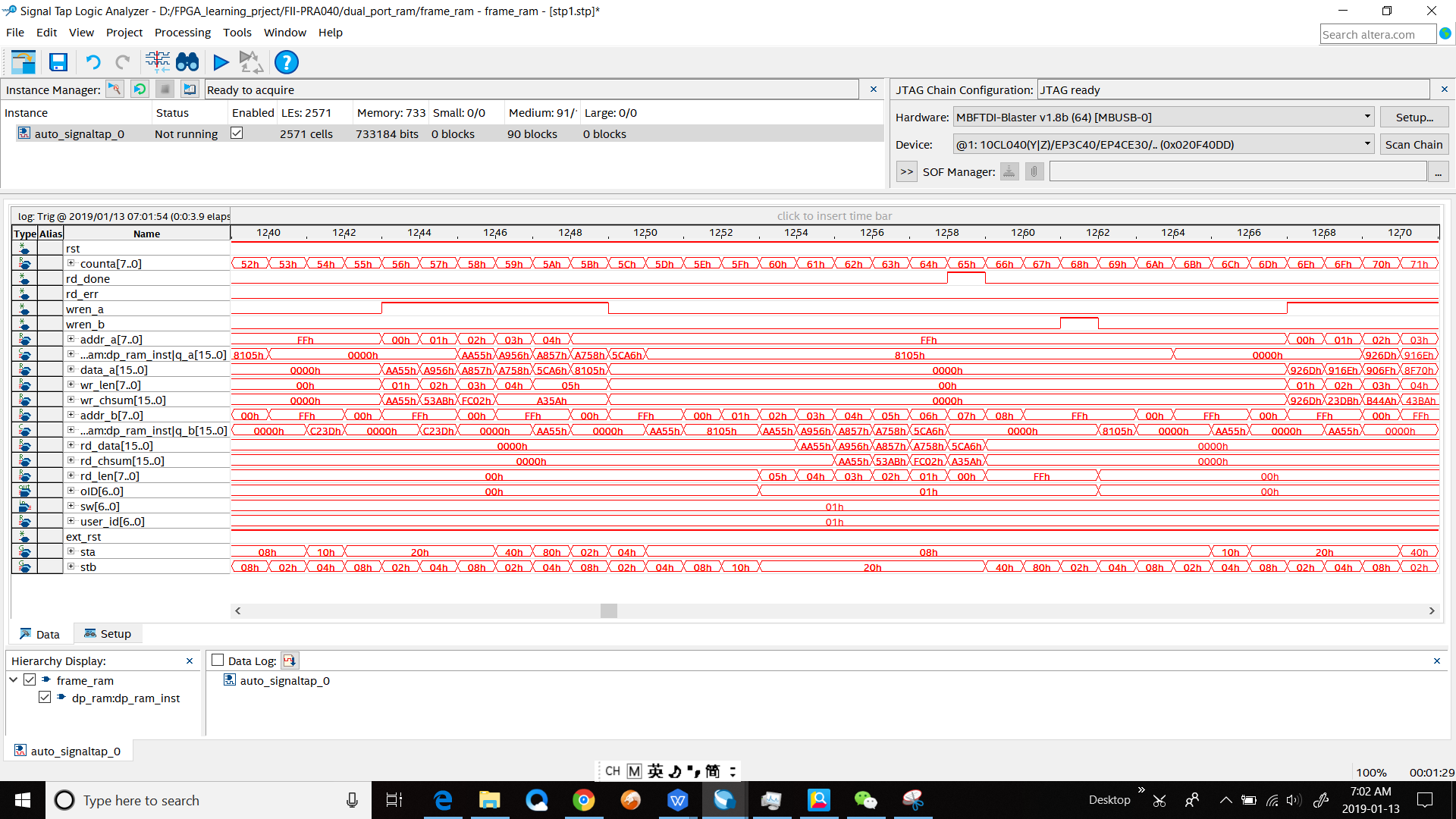
Figure 9.1 SignalTap II simulation
Experiment 10 Asynchronous Serial Port Design and Experiment
10.1 Experiment Objective
Because asynchronous serial ports are very common in industrial control, communication, and software debugging, they are also vital in FPGA development.
- Study the basic principles of asynchronous serial port communication, handshake mechanism and data frame structure
- Master asynchronous sampling techniques
- Review the frame structure of the data packet
- Learn to use FIFO
- Joint debugging with common debugging software of PC (SSCOM, Tera Term, etc.)
10.2 Experiment Implement
- Design and transmit full-duplex asynchronous communication interface Tx, Rx
- Baud rate of 11520 bps, 8-bit data, 1 start bit, 1 or 2 stop bits
- Receive buffer (Rx FIFO), transmit buffer (Tx FIFO)
- Forming a data packet
- Packet parsing
10.3 Experiment
10.3.1 Introduction to the UART Interface
A USB-B interface and a CP2102 chip are onboard for serial data communication.
The CP2102 features a high level of integration with a USB 2.0 full-speed function controller, USB transceiver, oscillator, EEPROM, and asynchronous serial data bus (UART) to support modem full-featured signals without the need for any external USB devices. See Figure 10.1 for the physical picture.
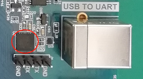
Figure 10.1 USB-B Interface and CP2102 Chip Physical Picture
10.3.2 Hardware Design
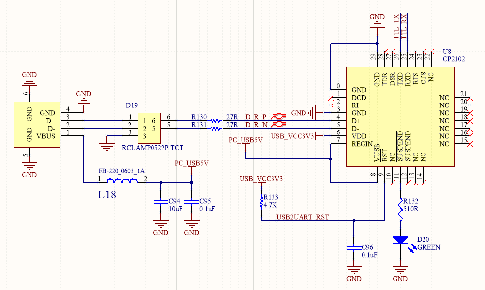
Figure 10.2 Schematics of the serial port
The principle of USB serial port conversion is shown in Figure 10.2. The TTL_TX and TTL_RX of the CP2102 are connected to the FPGA to transmit and receive data. After being processed internally by the chip, the D_R_P and D_R_N are connected to the USB interface through a protection chip, and the data is transmitted with the PC to implement serial communication.
10.3.3 Introduction of the Program
The first step: the main program architecture
|
There are a lot of handshake signals here, with the tx prefix for the transmit part of the signal, and the rx prefix is for the receive part of the signal.
Step 2: create a new baud rate generator file
- Input clock 7.3728MHz (64 times 115200). The actual value is 7.377049MHz, which is because the coefficient of the PLL is an integer division, while the error caused by that is not large, and can be adjusted by the stop bit in asynchronous communication. See Figure 10.3.
Fine solution
- Implemented with a two-stage PLL for a finer frequency
- The stop bit is set to be 2 bits, which can effectively eliminate the error.
This experiment will not deal with the precision. The default input frequency is 7.3728 MHz.
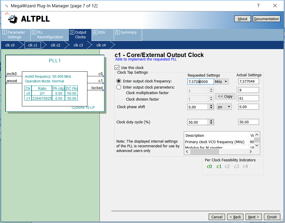
Figure 10.3 PLL setting
- Supported baud rates are 115200,57600,38400,19200
- The default baud rate is 115200
- Source file of designing baud rate
|
Four different gear positions are set to select the baud rate, corresponding to the step 2, (1). The baud rate of the receiving part is similar to that of the transmitting part.
Step 3: Design the send buffer file tx_buf
- 8-bit FIFO, depth is 256, read/write clock separation, write full flag, read empty flag
- Interface and handshake
- rst reset signal
- wr_clk write clock
- tx_clk send clock
- 8-bit write data tx_data
- wr_en write enable
- ctrl writes whether the input is a data or a control word
- rdy buffer ready, can accept the next data frame
Transmit buffer instantiation file
|
- Serial transmission, interface and handshake file design
- Interface design
- tx_rdy, send vacancy, can accept new 8-bit data
- tx_en, send data enable, pass to the sending module 8-bit data enable signal
- tx_data, 8-bit data to be sent
- tx_clk, send clock
- tx_baud, send baud rate
- Instantiation
|
- Write a testbench file to simulate the transmit module. (tb_uart)
- ModelSim simulation waveforms for transmit module. See Figure 10.4.
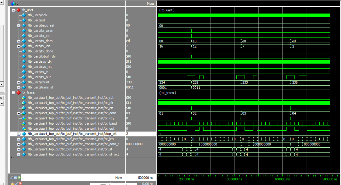
Figure 10.4 Serial port sending ModelSim simulation waveform
- Extended design (extended content is only reserved for users to think and practice)
- Design the transmitter to support 5, 6, 7, 8-bit PHY (Port physical layer)
- Support parity check
- The settings of the above steps involve FIFO, PLL, etc. (Refer to uart_top project file)
The fourth step: UART receiving module design
- Design of rx_phy.v
- Design strategies and steps
- Use 8 times sampling: so rx_baud is different from tx_baud, here sampling is rx_band = 8*tx_band
Adopting judgments to the receiving data
Determine whether the data counter is greater than 4 after the sampling value is counted.
- Steps to receive data:
- Synchronization: refers to how to find the start bit from the received 0101 (sync_dtc)
- Receive start bit (start)
- Cyclically receive 8-bit data
- Receive stop bit (determine whether it is one stop bit or two stop bits)
- Determine if the stop bit is correct
- Correct, jump to step B
- Incorrect, jump to step A, resynchronize
- Do not judge, jump directly to B, this design adopts the scheme of no judgment
- Design of rx_buf
- Design strategies and steps
- Add 256 depth, 8-bit fifo
- Read and write clock separation
- Asynchronous clear (internal synchronization)
- Data appears before the rdreq in the read port
- Steps:
- Initialization: fifo, rx_phy
- Wait: FIFO full signal (wrfull) is 0
- Write: Triggered by rx_phy_byte, rx_phy_rdy of rx_phy:
- End of writing
- Back to step b and continue to wait
- rx_buf.v source program (Reference to project files)
- Receive module simulation
Contents and steps
- tx, rx loopback test (assign rx_in = tx_out)
- Continue to use the testbench file in the tx section
- Write the testbench of rx
- ModelSim simulation. See Figure 10.5.
- Reflection and development
- Modify the program to complete the 5, 6, 7, 8-bit design
- Completing the design of the resynchronization when the start and stop have errors of the receiving end rx_phy
- Complete the analysis and packaging of the receiving data frame of rx_buf
- Using multi-sampling to design 180° alignment data sampling method, compare FPGA resources, timing and data recovery effects
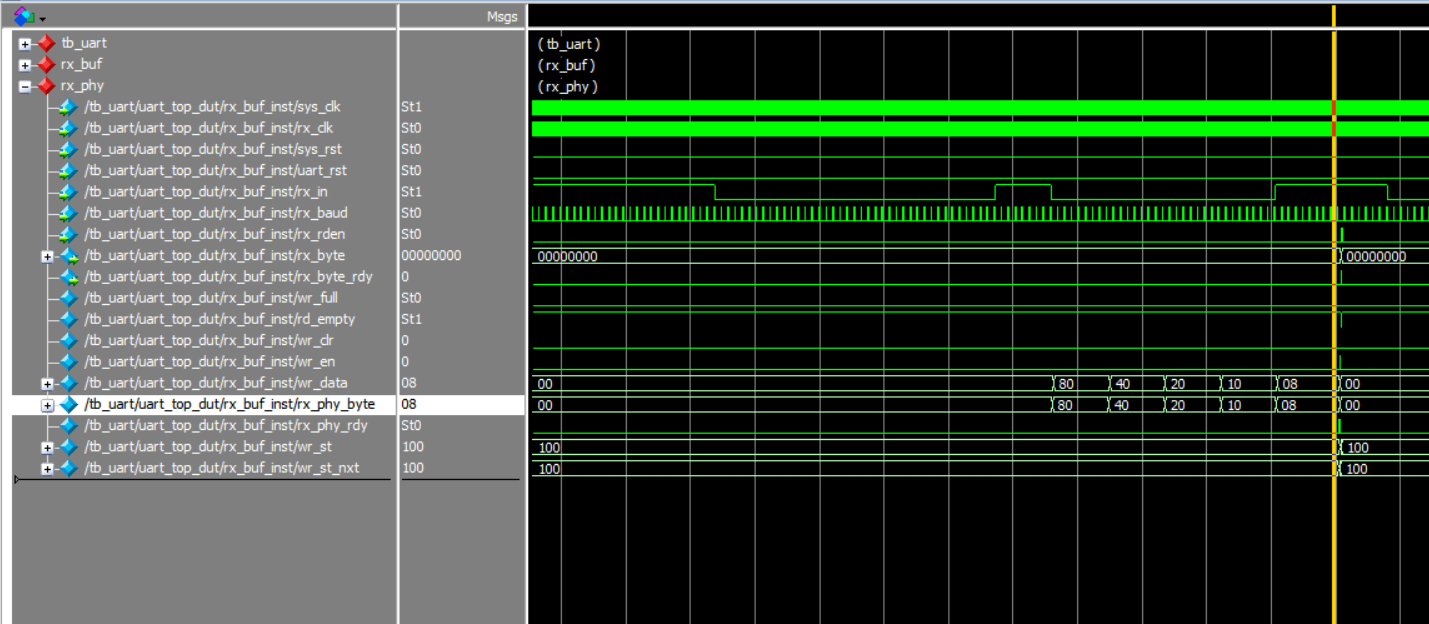
Figure 10.5 rx_phy wave form
10.4 Experiment Verification
- Hardware interface, FII-PRA040 development board has integrated USB to serial port conversion
UART chip
CP2102
RXD
USB
CON8
TXD
- Write a hardware test file
- Test plan: connect development board CON8 to host USB interface
- Using test software such as Tera Term, SSCOM3, etc., you can also write a serial communication program (C#, C++, JAVA, Python…)
- PC sends data in a certain format
- The test end uses a counter to generate data in a certain format.
- Write the test program hw_tb_uart and instantiate uart_top in it.
- Set hw_tb_uart to the top level, instantiate the previous program, and then verify it
- Pin assignments:
Table 10.1 Serial port experiment pin mapping
| Signal Name | Network Label | FPGA Pin | Port Description |
| Inclk | CLK_50M | G21 | Input clock |
| rst | KEY2 | Y6 | Reset signal |
| rx_in | TTL_RX | E16 | Serial data received |
| tx_out | TTL_TX | F15 | Serial data transmitted |
- Observe the experiment result
- Observe the data received by the PC. See in Figure 10.6.
- Observe the data received by the FPGA with SignalTap II
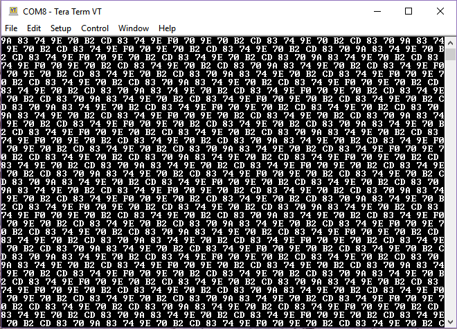
Figure 10.5 Data transmitted by FPGA displayed on the host computer
Experiment 11 IIC Protocol Transmission
11.1 Experiment Objective
- Learning the basic principles of asynchronous IIC bus, and the IIC communication protocol
- Master the method of reading and writing EEPROM
- Joint debugging using logic analyzer
11.2 Experiment Implement
- Correctly write a number to any address in the EEPROM (this experiment writes to the register of 8’h03 address) through the FPGA (here changes the written 8-bit data value by (SW7~SW0)). After writing in successfully, read the data as well. The read data is displayed directly on the segment display.
- Program the FPGA and press the left push button to execute the data write into EEPROM operation. Press the right push button to read the data that was just written.
- Determine whether it is correct or not by reading the displayed number on the segment display. If the segment display has the same value as written value, the experiment is successful.
- Analyze the correctness of the internal data with SignalTap II and verify it with the display of the segment display.
11.3 Experiment
11.3.1 Introduction of EEPROM and IIC Protocol
- Introduction of EEPROM
EEPROM (Electrically Erasable Programmable Read Only Memory) refers to a charged erasable programmable read only register. It is a memory chip that does not lose data after turning off power.
On the experiment board, there is an IIC interface EEPROM chip 24LC02 with a capacity of 256 bytes. Users can store some hardware configuration data or user information due to the characteristics that the data is not lost after power-off.
- The overall timing protocol of IIC is as follows
- Bus idle state: SDA, SCL are high
- Start of IIC protocol: SCL stays high, SDA jumps from high level to low level, generating a start signal
- IIC read and write data stage: including serial input and output of data and response signal issued by data receiver
- IIC transmission end bit: SCL is in high level, SDA jumps from low level to high level, and generates an end flag. See Figure 11.1.
- SDA must remain unchanged when SCL is high. It changes only when SCL is low
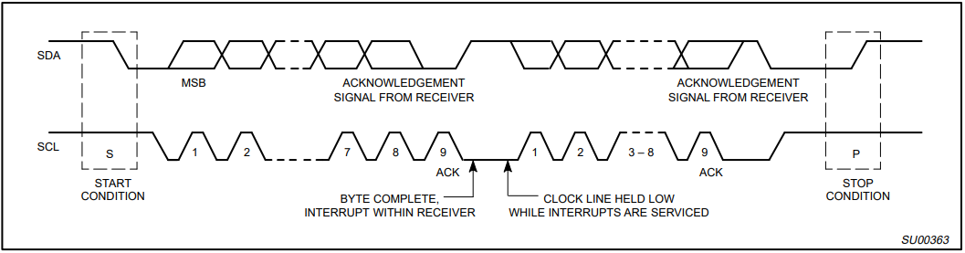
Figure 11.1 Timing protocol of IIC
11.3.2 Hardware Introduction
Each IIC device has a device address. When some device addresses are shipped from the factory, they are fixed by the manufacturer (the specific data can be found in the manufacturer’s data sheet). Some of their higher bits are determined, and the lower bits can be configured by the user according to the requirement. The higher four-bit address of the EEPROM chip 24LC02 used by the develop board has been fixed to 1010 by the component manufacturer. The lower three bits are linked in the develop board as shown below, so the device address is 1010000. See Figure 11.2. EEPROM reads and writes data from the FPGA through the I2C_SCL clock line and the I2C_SDA data line.
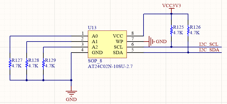
Figure 11.2 EEPROM schematics of IIC device
11.3.3 Introduction to the program
This experiment has two main modules, I2C reading and writing module and LED display module; The first module is mainly introduced here.
The first step: establishment of the main program framework
|
The input 8-bit data is needed to be written into the EEPROM, provided by an 8-bit DIP switch.
|
First, use the system 50 MHz clock to get a 100 kHz clock with a period of 10us by frequency division as the transmission clock of the IIC protocol. Then, the rising edge, the high state, the falling edge and the low state of the clock are defined by the counter, prepared for the subsequent data reading and writing and the beginning of the IIC protocol. The last line of code means to define a data valid signal. Only when the signal is high, that is, when the data is valid, the IIC clock is valid again, otherwise it is in high impedance. This is also set according to the IIC transport protocol.
The third step: specific implementation of I2C transmission
|
The entire process is implemented using a state machine. When reset, it is idle state, while data line sda_r is pulled high, clock and data are both valid, i.e. scl_link, sda_link are high; counter num is cleared and read_data is 0. 5ms delay counter is cleared, IIC transmission end signal Iic_done is low thus invalid.
- IDLE state: When receiving the read enable or write enable signal sw1_r || sw2_r, assign the write control word to the intermediate variable db_r <= `DEVICE_WRITE, and jump to the start state START1;
- START1 state: pull the data line low when the clock signal is high, generating the start signal of IIC transmission, and jump to the device address state ADD1;
- Device address status ADD1: After the write control word (device address plus one ‘0’ bit) is transmitted according to MSB (high order priority), the sda_link is pulled low causing data bus in a high impedance state, and jump to the first response state ACK1, waiting for the response signal from the slave (EEPROM).
- The first response status ACK1: If the data line is pulled low, it proves that the slave receives the data normally, otherwise the data is not written into EEPROM, and then the rewriting or stopping is decided by the user. There is no temporary judgment and processing here, jump directly to the write register address state ADD2, and assign the address BYTE_ADDR written to the intermediate variable (this experiment writes the data into the third register, i.e. BYTE_ADDR = 0000_0011)
- Register address status ADD2: Same as (3), it transfers register address to slave and jump to second response status ACK2
- The second response state ACK2: At this time, it is urgent to judge. If it is the write state sw1, it jumps to the data transfer state DATA, and at the same time assigns the written data to the intermediate variable. If it is the read state sw2, it jumps to the second start state START2 and assign the read control word to the intermediate variable.
- The second start state START2: it produces a start signal identical to (2) and jumps to the read register address state ADD3
- Read register address status ADD3: it jumps to the third response status ACK3S after the transfer of the register address that needs to be read out
- The third response state ACK3: it jumps directly to the data transfer state DATA. In the read state, the data to be read is directly read out immediately following the register address.
- Data transfer status DATA: it needs to be judged here. If it is the read status, the data will be directly output. If it is the write status, the data to be written will be transferred to the data line SDA. Both states need to jump to the fourth response state. ACK4
- The fourth response status ACK4: it direct jumps to stop transmission STOP1
- Stop transmission STOP1: it pulls up data line when the clock line is high, generating a stop signal, and jumps to the transfer completion status STOP2
- Transfer completion status STOP2: it releases all clock lines and data lines, and after a 5ms delay, returns to the IDLE state to wait for the next transfer instruction. This is because EEPROM stipulates that the interval between two consecutives read and write operations must not be less than 5ms.
11.4 Experiment Verification
The first step: pin assignments
Table 11.1 IIC protocol transmission experiment pin mapping
| Signal Name | Network Label | FPGA Pin | Port Description |
| clk | CLK_50M | G21 | System clock 50 MHz |
| rst_n | PB3 | Y6 | Reset |
| sm_db[0] | SEG_PA | B15 | Segment a |
| sm_db [1] | SEG_PB | E14 | Segment b |
| sm_db [2] | SEG_PC | D15 | Segment c |
| sm_db [3] | SEG_PD | C15 | Segment d |
| sm_db [4] | SEG_PE | F13 | Segment e |
| sm_db [5] | SEG_PF | E11 | Segment f |
| sm_db [6] | SEG_PG | B16 | Segment g |
| sm_db [7] | SEG_DP | A16 | Segment h |
| sm_cs1_n | SEG_3V3_D1 | D19 | Segment 1 |
| sm_cs2_n | SEG_3V3_D0 | F14 | Segment 0 |
| data [0] | SW0 | U11 | Switch input |
| data [1] | SW1 | V11 | Switch input |
| data [2] | SW2 | U10 | Switch input |
| data [3] | SW3 | V10 | Switch input |
| data [4] | SW4 | V9 | Switch input |
| data [5] | SW5 | W8 | Switch input |
| data [6] | SW6 | Y8 | Switch input |
| data [7] | SW7 | W6 | Switch input |
| sw1 | PB4 | AB4 | Write EEPROM button |
| sw2 | PB6 | AA4 | Read EEPROM button |
| scl | I2C_SCL | D13 | EEPROM clock line |
| sda | I2C_SDA | C13 | EEPROM data line |
Step 2: board verification
After the pin assignment is completed, the compilation is performed, and the board is verified after passing.
After the board is programmed, press the LEFT key to write the 8-bit value represented by SW7~SW0 to EEPROM. Then press the RIGHT key to read the value from the write position. Observe the consistency between the value displayed on the segment display on the experiment board and the value written in the 8’h03 register of the EEPROM address (SW7~SW0) (this experiment writes 8’h34). The read value is displayed on the segment display. The experimental phenomenon is shown in Figure 11.3.
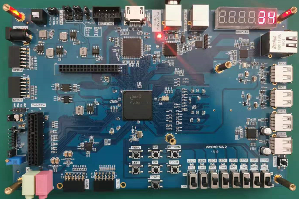
Figure 11.3 Observe experiment result
Experiment 12 AD, DA Experiment
12.1 Experiment Objective
Since in the real world, all naturally occurring signals are analog signals, and all that are read and processed in actual engineering are digital signals. There is a process of mutual conversion between natural and industrial signals (digital-to-analog conversion: DAC, analog-to-digital conversion: ADC). The purpose of this experiment is as follows:
- Learn about the theory of AD conversion
- Review the knowledge of the IIC protocol learned in the previous experiment and write the data into PCF8591 on the development board.
- Read the value of AD acquisition from PCF8591, and convert the value obtained into actual value, display it with segment display
12.2 Experiment Implement
- The ADC port of the chip is used for analog-to-digital conversion. The chip is correctly configured. Three variable (potentiometer, photoresistor, thermistor) voltages on the development board are collected, and the collected voltage value is displayed through the segment display.
- Board downloading verification, compared with resistance characteristics, verify the correctness of the results
12.3 Experiment
Introduction to AD Conversion Chip PCF8591
The PCF8591 is a monolithically integrated, individually powered, low power consuming, 8-bit CMOS data acquisition device. The PCF8591 has four analog inputs, one analog output, and one serial IIC bus interface. The three address pins A0, A1 and A2 of the PCF8591 can be used for hardware address programming. The address, control signals and data signals of the input and output on the PCF8591 device are transmitted serially via the two-wire bidirectional IIC bus. Please refer to the previous experiment 11 for the contents of the IIC bus protocol. After the device address information and the read/write control word are sent, the control word information is sent.
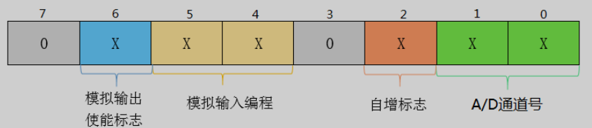
Analog Input Selection
A/D Channel Number
Automatic Gain Flag
Analog Output Enable
Figure 12.1 PCF8591 address
The specific control word information is shown in Figure 12.1. Digit 1 – digit 0 is used for four channel settings, digit 2 is for automatic gain selection, ‘1’ is valid. Digit 5 – digit 4 determines analog input selection. Digit 6 is analog output enable. Digit 7 and digit 3 are reserved to be ‘0’. The second byte sent to PCF8951 is stored in the control register to control the device functionality. The upper nibble of the control register is used to allow the analog output to be programmed as a single-ended or differential input. The lower nibble selects an analog input channel defined by the high nibble. If the auto increment flag is set to 1, the channel number will be automatically incremented after each A/D conversion.
In this experiment, the input channel is selected as the AD acquisition input channel by using the DIP switch (SW1, SW0). The specific channel information is shown in Table 12.1. The control information is configured as 8’h40, which is the analog output, and defaults to “00” channels, which means that the photoresistor voltage value is displayed by default.
Table 12.1 Channel information
| SW1,SW0 | Channel Selection | Acquisition Object |
| 00 | 0 | Voltage of photoresistor |
| 01 | 1 | Voltage of thermistor |
| 10 | 2 | Voltage of potentiometer |
Hardware Design
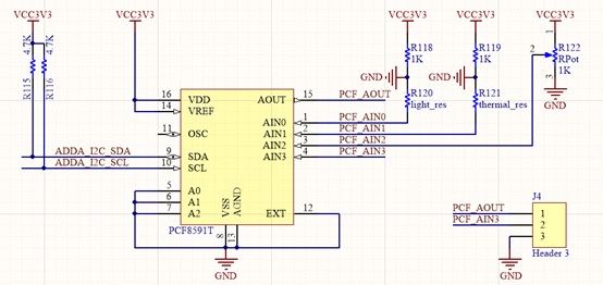
Figure 12.2 Schematics of the AD/DA converter
The schematics of AD/DA conversion using PCF8591 is shown in Figure 12.2. The IIC bus goes through two pull-up resistors and pulls high when not working. A0, A1, A2 are grounded, so the device address is 7’b1010000, the analog input channel AIN0 is connected to the photoresistor, AIN1 is connected to the thermistor, and AIN3 is connected to the potentiometer. When the channel is selected, FPGA will read the value in PCF8591 through the data bus ADDA_I2C_SLC for processing.
Introduction to the Program
This experiment also uses the IIC bus to control the PCF8951 chip, so the program is basically the same as Experiment 11. Only parts difference from Experiment 11 are indicated here.
|
The role of this part is that when the chip continuously collects the voltage value across the resistor, due to a series of unstable factors, the voltage value will be unstable, so the output value will have a large error, so 16 sets of data is collected each time, then gets averaged, and the result is output as the voltage value across the resistor at this time. Then, by the change of the voltage value, it is possible to judge the regular pattern. Such as photoresistor, the greater the light intensity, the smaller the voltage value, the smaller the resistance value, satisfying the photoresistor characteristics; the higher the thermistor temperature, the smaller the voltage value, the smaller the resistance, satisfying the photoresistor characteristics; the potentiometer rotates clockwise, and the voltage increases, the resistance increases; counterclockwise rotating decreases the voltage, and the resistance decreases.
The maximum output of the AD chip is an 8-bit digital quantity, but in fact it is not the required voltage value. It quantifies the voltage value of the range into 256 portions (8-bit binary number can represent 256 decimal numbers), so further calculations and conversions needs to be applied when displaying on the segment display.
|
VCC is 3.3V, so the maximum resistance voltage is 3.3V. The 8-bit data dis_data is multiplied by 3300 and assigned to numt by 1000 times, which is convenient for display and observation. The numt is further reduced by 256 times (left shifting 8 bits) to num1, corresponding to 256 quantitized portions of PCF8951. num1 at this time is 1000 times the voltage value of two ends of the resistor. Display each digit on the segment display, in the order of high to low (data5 to data0) and add the decimal point (data3) to digit of thousands. At this time, the value displayed by the segment display is the voltage across the resistor value and correct to 3 decimal places.
12.4 Experiment Verification
The first step: assign the pin
Table 12.2 AD conversion experiment pin mapping
| Signal Name | Network Label | FPGA Pin | Port Description |
| clk | CLK_50M | G21 | System clock 50 MHz |
| rst_n | PB3 | Y6 | Reset |
| sm_db[0] | SEG_PA | B15 | Segment a |
| sm_db [1] | SEG_PB | E14 | Segment b |
| sm_db [2] | SEG_PC | D15 | Segment c |
| sm_db [3] | SEG_PD | C15 | Segment d |
| sm_db [4] | SEG_PE | F13 | Segment e |
| sm_db [5] | SEG_PF | E11 | Segment f |
| sm_db [6] | SEG_PG | B16 | Segment g |
| sm_db [7] | SEG_DP | A16 | Segment h |
| sel[0] | SEG_3V3_D0 | F14 | Bit selection 0 |
| sel[1] | SEG_3V3_D1 | D19 | Bit selection 1 |
| sel[2] | SEG_3V3_D2 | E15 | Bit selection 2 |
| sel[3] | SEG_3V3_D3 | E13 | Bit selection 3 |
| sel[4] | SEG_3V3_D4 | F11 | Bit selection 4 |
| sel[5] | SEG_3V3_D5 | R12 | Bit selection 5 |
| data[0] | SW0 | U11 | Swicth input |
| data[1] | SW1 | V11 | Swicth input |
| data[2] | SW2 | U10 | Swicth input |
| data[3] | SW3 | V10 | Swicth input |
| data[4] | SW4 | V9 | Swicth input |
| data[5] | SW5 | W8 | Swicth input |
| data[6] | SW6 | Y8 | Swicth input |
| data[7] | SW7 | W6 | Swicth input |
| scl | ADDA_I2C_SCL | C20 | PCF8591 clock line |
| sda | ADDA_I2C_SDA | D20 | PCF8591 data line |
Step 2: board verification
After the pin assignment is completed, the compilation is performed, and board is verified after passing.
Under the default state, that is, the channel selection is “00”, the segment display shows the current ambient brightness state, the voltage value across the photoresistor is 2.010V, as shown in Figure 12.3.
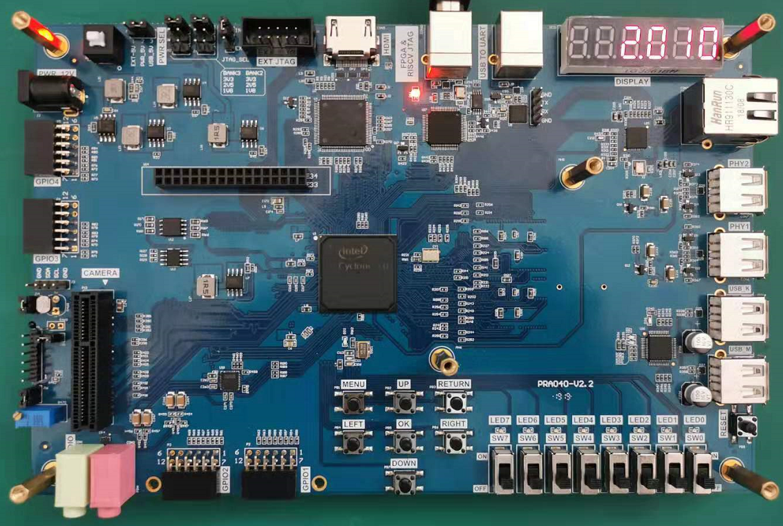
Figure 12.3 Photoresistor test phenomenon
When the channel selection is “01”, the segment display shows the current ambient temperature, the voltage across the thermistor is 2.926V, as shown in Figure 12.4.
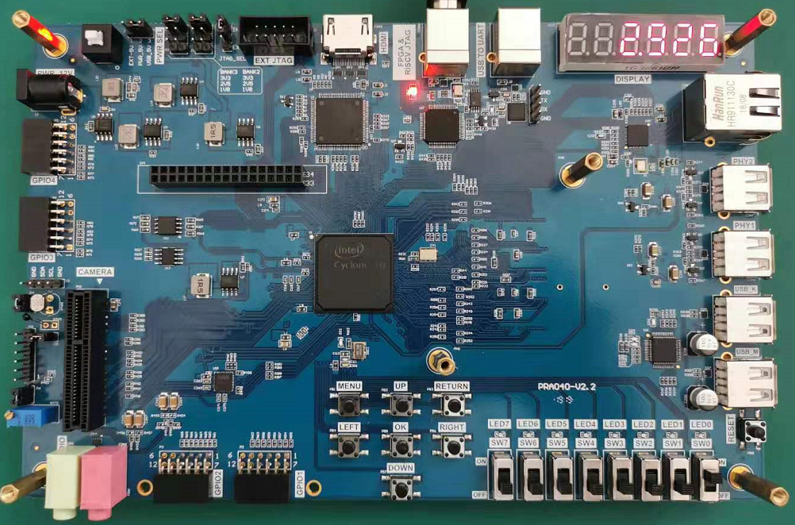
Figure 12.4 Thermistor experiment phenomenon
When the channel is selected as “10”, the segment display shows the current resistance value, and the voltage across the potentiometer is 1.456 V, as shown in Figure 12.5.
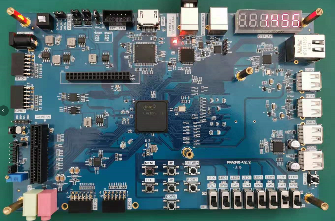
Figure 12.5 Potentiometer experiment phenomenon
Experiment 13 HDMI Display
13.1 Experiment Objective
- Review IIC protocol
- Review EEPROM read and write
- Learn HDMI principle
13.2 Experiment Implement
Display different image content on the screen through the HDMI.
13.3 Experiment
13.3.1 Introduction to HDMI and ADV7511 Chip
Image display processing has always been the focus of FPGA research. At present, the image display mode is also developing. The image display interface is also gradually transitioning from the old VGA interface to the new DVI or HDMI interface. HDMI (High Definition Multimedia Interface) is a digital video/audio interface technology. It is a dedicated digital interface for image transmission. It can transmit audio and video signals at the same time.
The ADV7511 is a chip that converts FPGA digital signal to HDMI signal following VESA standard. For more details, see the related chip manual. Among them, “ADV7511 Programming Guide” and “ADV7511 Hardware Users Guide” are the most important. The registers of the ADV7511 can be configured by referring those documents.
ADV7511 Register Configuration Description: The bus inputs D0-D3, D12-D15, and D24-D27 of the ADV7511 have no input, and each bit of data is in 8-bit mode. Directly set 0x15 [3:0]) 0x0 data, 0x16 [3:2] data does not need to be set for its mode. Set [5:4] of 0X16 to 11for 8-bit data and keep the default values for the other digits. 0x17[1] refers to the ratio of the length to the width of the image. It can be set to 0 or 1. The actual LCD screen will not change according to the data but will automatically stretch the full screen mode according to the LCD’s own settings. 0x18[7] is the way to start the color range stretching. The design is that RGB maps directly to RGB, so it can be disabled directly. 0X18[6:5] is also invalid currently. 0XAF [1] is to set HDMI or DVI mode, the most direct point of HDMI than DVI is that HDMI can send digital audio data and encrypted data content. This experiment only needs to Display the picture, and it can be set directly to DVI mode. Set 0XAF [7] to 0 to turn off HDMI encryption. Due to GCCD, deep color encryption data is not applicable, so the GC option is turned off. 0x4c register does not need to be set as well. Other sound data setting can be ignored here for DVI output mode. After writing these registers, the image can be displayed successfully.
13.3.2 Hardware Design
The onboard HDMI module consists of an HDMI interface and an ADV7511 chip. The physical photo is shown in Figure 13.1. The schematics is shown in Figure 13.2.
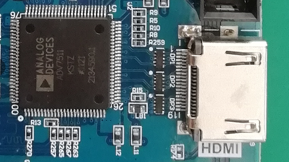
Figure 13.1 HDMI interface and ADV7511 chip physical photo
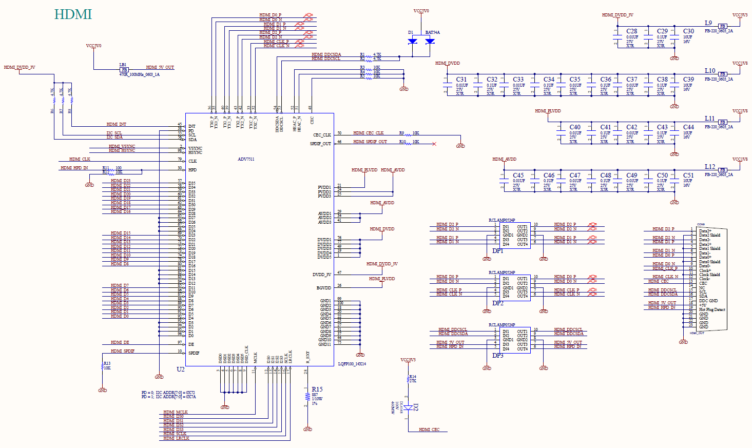
Figure 13.2 Schematics of HDMI
ADV7511 chip is set through the IIC bus and send the picture information to be displayed to the chip through HDMI_D0 to HDMI_D23, and control signals HDMI_HSYNC and HDMI_VSYNC and the clock signal HDMI_CLK, which are transmitted to the PC through the HDMI interface after being processed internally by the chip.
13.3.3 Introduction to the Program
The configuration part of the ADV7511 chip is carried out using the IIC protocol, with reference to Experiment 11 and Experiment 12. A brief introduction to the data processing section is now available.
|
The FPGA configures the ADV7511 chip through the IIC bus (clock line scl, data line sda). After the configuration is completed, the output image information needs to be determined. Taking the 1080P (1920*1080) image format as an example, it outputs data signal rgb_r (red component), rgb_g (green component), rgb_b (blue component), a line sync signal rgb_hs, a field sync signal rgb_vs, and a clock rgb_clk signal. Each pixel is formed by a combination of three color components. Each row of 1920 pixels is filled with color information in a certain order (from left to right) and begin to fill the next line after completing one line, in a certain order (from top to bottom) to finish 1080 lines, so that one frame of image information is completed. The image information of each frame is determined by this horizontal and vertical scanning, and then transmitted to the ADV7511 for processing. The timing diagram of the horizontal and vertical scan is shown in Figure 13.3, Figure 13.4.
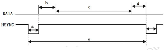
Figure 13.3 Horizontal synchronization
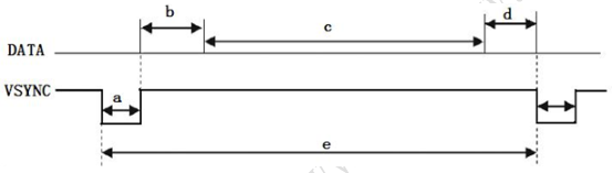
Figure 13.4 Vertical synchronization
The second step: data definition of 1080p image timing generation
|
The third step: Generate display content
|
When the button is pressed, a key1 signal will be input, and the content displayed on the screen will change according to the change of vga_dis_mode, and the corresponding picture content will be displayed.
13.4 Experiment Verification
The first step: pin assignment
Table 13.1 HDMI Experiment Pin Mapping
| Signal Name | Network Label | FPGA Pin | Port Description |
| clk | CLK_50M | G21 | System clock 50 MHz |
| rst_n | PB3 | Y6 | Reset |
| en | HDMI_R_DE | A8 | Enable |
| scl | I2C_SCL | D13 | IIC clock line |
| sda | I2C_SDA | C13 | IIC data line |
| key1 | PB2 | V5 | Switch display content |
| vga_clk | HDMI_R_CLK | E5 | HDMI clock |
| vga_hs | HDMI_R_HS | B9 | Horizontal sync signal |
| vg_vs | HDMI_R_VS | A9 | Vertical sync signal |
| vga_b[0] | HDMI_R_D0 | A7 | Blue output |
| vga_b[1] | HDMI_R_D1 | B8 | |
| vga_b[2] | HDMI_R_D2 | E9 | |
| vga_b[3] | HDMI_R_D3 | B7 | |
| vga_b[4] | HDMI_R_D4 | C8 | |
| vga_b[5] | HDMI_R_D5 | C6 | |
| vga_b[6] | HDMI_R_D6 | F8 | |
| vga_b[7] | HDMI_R_D7 | B6 | |
| vga_g[0] | HDMI_R_D8 | A5 | Green output |
| vga_g[1] | HDMI_R_D9 | C7 | |
| vga_g[2] | HDMI_R_D10 | D7 | |
| vga_g[3] | HDMI_R_D11 | B5 | |
| vga_g[4] | HDMI_R_D12 | C6 | |
| vga_g[5] | HDMI_R_D13 | A4 | |
| vga_g[6] | HDMI_R_D14 | D6 | |
| vga_g[7] | HDMI_R_D15 | B4 | |
| vga_r[0] | HDMI_R_D16 | E7 | Red output |
| vga_r[1] | HDMI_R_D17 | A3 | |
| vga_r[2] | HDMI_R_D18 | C4 | |
| vga_r[3] | HDMI_R_D19 | B3 | |
| vga_r[4] | HDMI_R_D20 | C3 | |
| vga_r[5] | HDMI_R_D21 | F7 | |
| vga_r[6] | HDMI_R_D22 | F9 | |
| vga_r[7] | HDMI_R_D23 | G7 |
The second step: board verification
After the pin assignment is completed, the compilation is performed, and the development board is programmed.
Press the push button and the display content changes accordingly. The experimental phenomenon is shown in the figure below (only a few are listed).

Figure 13.5 HDMI display (all white)

Figure 13.6 HDMI display (square)

Figure 13.7 HDMI display (color strip)
Experiment 14 Ethernet
14.1 Experiment Objective
Understand what Ethernet is and how it works- Familiar with the relationship between different interface types (MII, GMII, RGMII) and their advantages and disadvantages (FII-PRA040 uses RGMII)
- Combine the development board to complete the transmission and reception of data and verify it
14.2 Experiment Implement
- Perform a loopback test to check if the hardware is working properly.
- Perform data receiving verification
- Perform data transmission verification
14.3 Experiment
14.3.1 Introduction to Experiment Principle
Ethernet is a baseband LAN technology. Ethernet communication is a communication method that uses coaxial cable as a network media and uses carrier multi-access and collision detection mechanisms. The data transmission rate reaches 1 Gbit/s, which can satisfy the need for data transfer of non-persistent networks. As an interconnected interface, the Ethernet interface is very widely used. There are many types of Gigabit Ethernet MII interfaces, and GMII and RGMII are commonly used.
MII interface has a total of 16 lines. See Figure 14. 1.
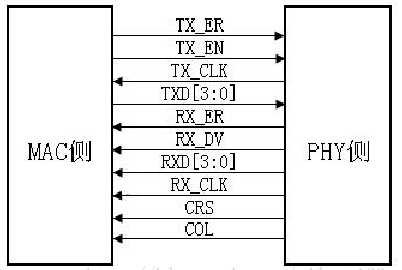
PHY SIDE
MAC SIDE
RXD(Receive Data)[3:0]: data reception signal, a total of 4 signal lines;
TX_ER(Transmit Error): Send data error prompt signal, synchronized to TX_CLK, active high, indicating that the data transmitted during TX_ER validity period is invalid. For 10Mbps rate, TX_ER does not work;
RX_ER(Receive Error): Receive data error prompt signal, synchronized to RX_CLK, active high, indicating that the data transmitted during the valid period of RX_ER is invalid. For 10 Mbps speed, RX_ER does not work;
TX_EN(Transmit Enable): Send enable signal, only the data transmitted during the valid period of TX_EN is valid;
RX_DV(Reveive Data Valid): Receive data valid signal, the action type is TX_EN of the transmission channel;
TX_CLK: Transmit reference clock, the clock frequency is 25 MHz at 100 Mbps, and the clock frequency is 2.5 MHz at 10 Mbps. Note that the direction of TX_CLK clock is from the PHY side to the MAC side, so this clock is provided by the PHY;
RX_CLK: Receive data reference clock, the clock frequency is 25 MHz at 100 Mbps, and the clock frequency is 2.5 MHz at 10 Mbps. RX_CLK is also provided by the PHY side;
CRS: Carrier Sense, carrier detect signal, does not need to synchronize with the reference clock. As long as there is data transmission, CRS is valid. In addition, CRS is effective only if PHY is in half-duplex mode;
COL: Collision detection signal, does not need to be synchronized to the reference clock, is valid only if PHY is in half-duplex mode.
GMII interface is shown in Figure 14. 2.
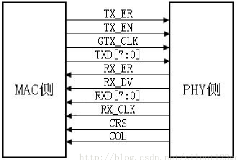
PHY SIDE
MAC SIDE
Figure 14.2 GMI Interface
Compared with the MII interface, the data width of the GMII is changed from 4 bits to 8 bits. The control signals in the GMII interface such as TX_ER, TX_EN, RX_ER, RX_DV, CRS, and COL function the same as those in the MII interface. The frequencies of transmitting reference clock GTX_CLK and the receiving reference clock RX_CLK are both 125 MHz (1000 Mbps / 8 = 125 MHz).
There is one point that needs special explanation here, that is, the transmitting reference clock GTX_CLK is different from the TX_CLK in the MII interface. The TX_CLK in the MII interface is provided by the PHY chip to the MAC chip, and the GTX_CLK in the GMII interface is provided to the PHY chip by the MAC chip. The directions are different.
In practical applications, most GMII interfaces are compatible with MII interfaces. Therefore, the general GMII interface has two transmitting reference clocks: TX_CLK and GTX_CLK (the directions of the two are different, as mentioned above). When used as the MII mode, TX_CLK and 4 of the 8 data lines are used.
See Figure 14.3 for RGMII interface.
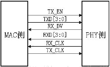
PHY SIDE
MAC SIDE
Figure 14.3 RGMII interface
RGMII, or reduced GMII, is a simplified version of GMII, which reduces the number of interface signal lines from 24 to 14 (COL/CRS port status indication signals, not shown here), the clock frequency is still 125 MHz, and the TX/RX data width is changed from 8 to 4 bits. To keep the transmission rate of 1000 Mbps unchanged, the RGMII interface samples data on both the rising and falling edges of the clock. TXD[3:0]/RXD[3:0] in the GMII interface is transmitted on the rising edge of the reference clock, and TXD[7:4]/RXD[7:4] in the GMII interface is transmitted on the falling edge of the reference clock. RGMI is also compatible with both 100 Mbps and 10 Mbps rates, with reference clock rates of 25 MHz and 2.5 MHz, respectively.
The TX_EN signal line transmits TX_EN and TX_ER information, TX_EN is transmitted on the rising edge of TX_CLK, and TX_ER is transmitted on the falling edge. Similarly, RX_DV and RX_ER are transmitted on the RX_DV signal line, and RX_DV is transmitted on the rising edge of RX_CLK, and RX_ER is transmitted on the falling edge.
14.3.2 Hardware Design
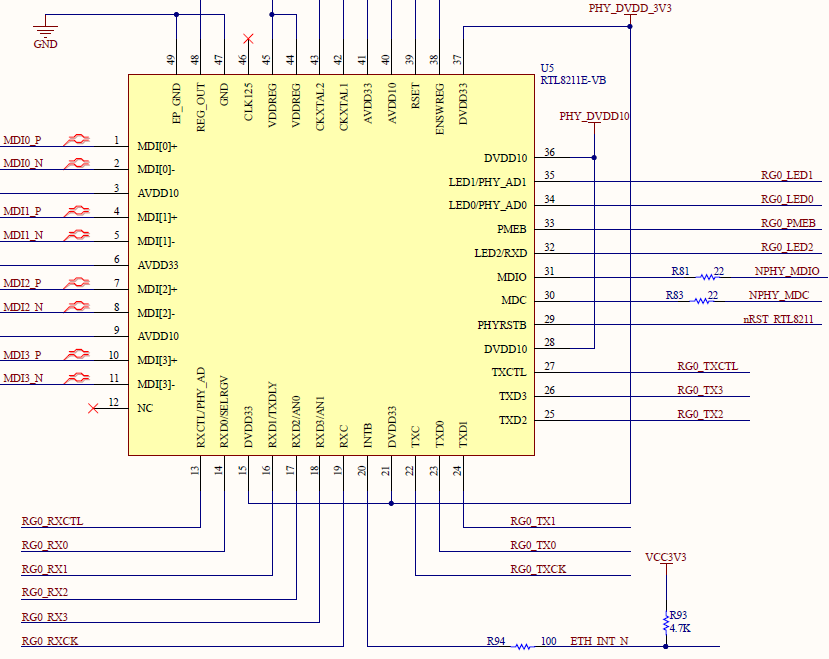
Figure 14.4 Schematics of RTL8211E-VB
The RTL8211E-VB chip is used to form a Gigabit Ethernet module on the experiment board. The schematics is shown in Figure 14.4. The PHY chip is connected to the FPGA by receiving and transmitting two sets of signals. The receiving group signal prefix is RG0_RX, and the transmitting group signal prefix is RG0TX, which is composed of a control signal CTL, a clock signal CK and four data signals 3-0. RG0_LED0 and RG0_LED1 are respectively connected to the network port yellow signal light and green signal light. At the same time, the FPGA can configure the PHY chip through the clock line NPHY_MDC and the data line NPHY_MDIO.
14.3.3 Design of the Program
- Loopback test design (test1)
The first step: introduction to the program
The loopback test is very simple, which just needs to output the input data directly.
|
(Note: Each program in this experiment contains a smi_ctrl module. In the config folder, it is a setting module for the PHY chip, so as to solve the problem that some computers cannot connect to the network port normally, and will not explain in detail)
The second step: pin assignment
Table 14.1 Ethernet Experiment Pin Mapping
| Signal Name | Network Label | FPGA Pin | Port Description |
| rxc | RGMII_RXCK | B12 | Input data clock |
| rxdv | RGMII_RXCTL | A13 | Input data control signal |
| rxd[3] | RGMII_RX3 | A15 | Input data bit 3 |
| rxd[2] | RGMII_RX2 | B14 | Input data bit 2 |
| rxd[1] | RGMII_RX1 | A14 | Input data bit 1 |
| rxd[0] | RGMII_RX0 | B13 | Input data bit 0 |
| txc | RGMII_TXCK | B20 | Output data clock |
| txen | RGMII_TXCTL | A19 | Output data control signal |
| txd[3] | RGMII_TX3 | B18 | Output data bit 3 |
| txd[2] | RGMII_TX2 | A18 | Output data bit 2 |
| txd[1] | RGMII_TX1 | B17 | Output data bit 1 |
| txd[0] | RGMII_TX0 | A17 | Output data bit 0 |
| e_mdc | NPHY_MDC | C17 | Configuration clock |
| e_mdio | NPHY_MDIO | B19 | Configuration data |
Before verification (the default PC NIC is a Gigabit NIC, otherwise it needed to be replaced). PC IP address needs to be confirmed first. In the DOS command window, type ipconfig -all command to check it. Example is shown in Figure 14. 5.
Figure 14.5 PC end IP information
To facilitate subsequent experiments, PC is provided a fixed IP address. Take this experiment as an example, IP configuration is 192.169.0.100(could be revised, but needs to be consistent to the IP address of target sending module, for Internet Protocol reason, IP address 169.XXX.X.X is not suggested). Find Internet Protocol Version 4(TCP/IPv4) in Network and Sharing center. See Figure 14. 6.
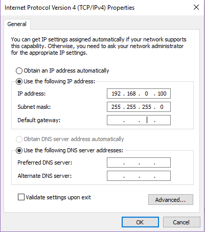
Figure 14.6 Configure PC end IP address
Since there is no ARP protocol content (binding IP address and MAC address of the develop board) in this experiment, it needs to be bound manually through the DOS command window. Here, the IP is set to 192.168.0.2 and the MAC address is set to 00-0A-35-01-FE-C0, (can be replaced by yourself) as shown in Figure 14. 7, the method is as follows: (Note: Run the DOS command window as an administrator)
Run the command: ARP -s 192.168.0.2 00-0A-35-01-FE-C0
View binding results: ARP -a
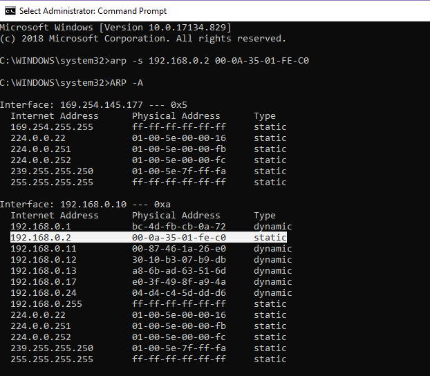
Figure 14.7 Address binding method 1
If a failure occurs while running the ARP command, another way is available, as shown in Figure 14.8:
- Enter the netsh i i show in command to view the number of the local connection, such as the “23” of the computer used this time.
- Enter netsh -c “i i” add neighbors 23 (number) “192.168.0.2” “00-0A-35-01-FE-C0”
- Enter arp -a to view the binding result
Figure 14.8 Address binding method 2
Next, we also use the DOS command window for connectivity detection, as shown in Figure 14. 9. Ping is an executable command that comes with the Windows family. Use it to check if the network can be connected. It can help us analyze and determine network faults. Application format: Ping IP address (not host computer IP).
Start SignalTap II, after sending the command, as shown in Figure 14. 10. The data is ordinary and the hardware is intact seen from the screenshot.
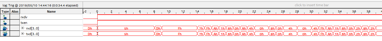
Figure 14.10 SignalTap II data capture
- Special IP core configuration (test2)
Because it is the RGMII interface, the data is bilateral along 4-bit data. Therefore, when data processing is performed inside the FPGA, it needs to be converted into 8-bit data. Go to Installed IP > Library > Basic Functions > I/O to find ALTDDIO_IN and ALTDDIO_OUT. To implement it, IP core (ddio_in) is called, and after internal data processing, IP core is passed (ddio_out) to convert 8-bit data into bilateral edge 4-bit data transfer. It should be noted that, considering the enable signal and data signal synchronization, the enable signal is entered to ddio for conversion at the same time. The specific settings are shown in Figure 14. 11 and Figure 14. 12.
Figure 14.11 ddio_in setting
Figure 14.12 ddio_out setting
Considering that the driving ability of the clock provided by the PHY chip is relatively poor, after the phase-locked loop processing, unlike the prior part, the input clock rxc selects the homologous input, as shown in Figure 14. 13, and outputs C0 clock ddio_clk as the driving clock of two ddio IP cores. As shown in Figure 14. 14, outputs the C1 clock txc as the data transmission clock (note that due to hardware circuit and timing reasons, txc needs to be 90° phase difference). See Figure 14. 15.
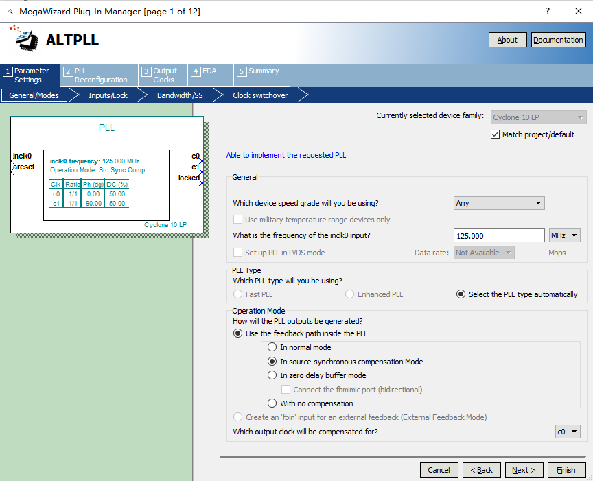
Figure 14.13 PLL input clock setting
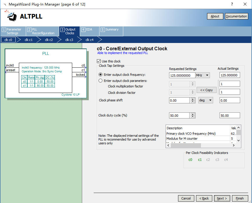
Figure 14.14 PLL output clcok(c0) setting
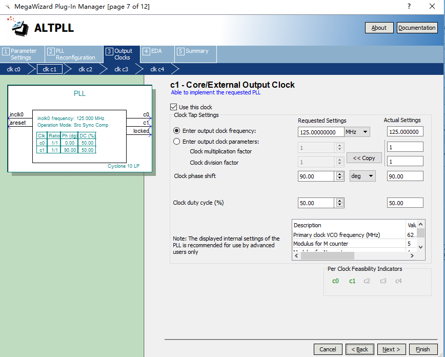
Figure 14.15 PLL output clcok(c1) setting
The three IP cores are instantiated into the previous loopback test, and the data transmission correctness test is performed. (It is necessary to notice the ordered timing. The ddio_out input data needs to be reversed. For details, refer to the project file (test2)). This time a network debugging assistant applet is used as an auxiliary testing tool. Program the board and verify it.
As shown in Figure 14.16, after setting the correct address and data type, we send the detection information (love you!) through the host computer. The data packet is captured by Wireshark, as shown in Figure 14.17. The data is correctly transmitted back to the PC.
Figure 14.16 Host computer sends the test data
Figure 14.17 Correct reception of data on the PC side
- Complete Ethernet data transmission design
For complete Ethernet data transmission, it is necessary to have the receiving part of the data and the transmitting part of the data. For the convenience of experiment, we store the data transmitted by the PC first in the RAM. After reading via the transmitting end, send it to the PC. For a series of data unpacking and packaging, refer to the project file “ethernet”. A brief introduction to each module follows.
- Data receiving module (ip_receive)
The problem to be solved by this module is to detect and identify the data frame, unpack the valid data frame, and store the real data in the ram.
|
The receiving module is to perform step by step analysis on the received data.
Idle state: If ‘55’ is received, it jumps to the six_55 state.
Six_55 state: If it continues to receive six consecutive 55s, it will jump to the spd_d5 state, otherwise it will return the idle state.
Spd_d5 state: If ‘d5’ continues received, it proves that the complete packet preamble “55_55_55_55_55_55_55_d5” has been received, and jumps to rx_mac, otherwise it returns the idle transition.
rx_mac state: This part is the judgment of the target MAC address and the source MAC address. If it matches, it will jump to the rx_IP_Protocol state, otherwise it will return the idle state and resend.
rx_IP_Protocol state: Determine the type and length of the packet and jump to the rx_IP_layer state.
rx_IP_layer state: Receive 20 bytes of UDP virtual header and IP address, jump to rx_UDP_layer state
rx_UDP_layer state: Receive 8-byte UDP port number and UDP packet length, jump to rx_data state
Rx_data state: Receive UDP data, jump to rx_finish state
Rx_finish state: A packet of data is received, and it jumps to the idle state to wait for the arrival of the next packet of data.
- Data sending module (ip_send)
The main content of this module is to read out the data in the RAM, package and transmit the data with the correct packet protocol type (UDP). Before transmitting, the data is also checked by CRC.
|
This part defines the preamble of the data packet, the MAC address of the PC, the MAC address of the development board, and the IP packet type. It should be noted that in the actual experiment, the MAC address of the PC needs to be modified. Keep the MAC address consistent along the project, otherwise the subsequent experiments will not receive data.
|
Idle state: Waiting for delay, sending a packet at regular intervals and jumping to the start state.
Start state: Send the packet header and jump to the make state.
make state: Generates the checksum of the header and jumps to the send55 state.
Send55 status: Send 8 preambles and jump to the sendmac state.
sendmac state: Send the target MAC address, source MAC address and IP packet type, and jump to the sendheader state.
sendheader state: Sends 7 32-bit IP headers and jumps to the senddata state.
senddata state: Send UDP packets and jump to the sendcrc state.
sendcrc state: Sends a 32-bit CRC check and returns the idle state.
Following the above procedure, the entire packet of data is transmitted, and the idle state is returned to wait for the transmission of the next packet of data.
- CRC check module (crc)
The CRC32 check of an IP packet is calculated at the destination MAC Address and until the last data of a packet. The CRC32 verilog algorithm and polynomial of Ethernet can be generated directly at the following website: http://www.easics.com/webtools/crctool
- UDP data test module (UDP)
This module only needs to instantiate the first three sub-modules together. Check the correctness of each connection.
- Top level module settings (ethernet)
The PLL, ddio_in, ddio_out, ram, and UDP modules are instantiated to the top level entity, and specific information is stored in advance in the RAM (Welcome To ZGZNXP World!). When there is no data input, the FPGA always sends this information. With data input, the received data is sent. Refer to the project files for more information.
14.4 Experiment Verification
The pin assignment of this test procedure is identical to that in Test 1.
Before programming the development board, it is necessary to note that the IP address of the PC and the MAC address of the development board must be determined and matched, otherwise the data will not be received.
Download the compiled project to the development board. As shown in Figure 14.18, the FPGA is keeping sending information to the PC. The entire transmitted packet can also be seen in Wireshark, as shown in Figure 14.19.
Figure 14.18 Send specific information
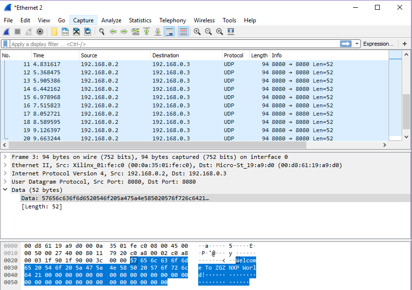
Figure 14.19 Specific information package
When the PC sends data to the FPGA, as shown in Figure 14. 20, the entire packet arrives at the FPGA, and then the FPGA repackages the received data and sends it to the PC. See Figure 14. 21, the network assistant also receives the transmitted data information accurately, as shown in Figure 14. 22. Similarly, through SignalTap we can see the process of writing the received data, as shown in Figure 14. 23.
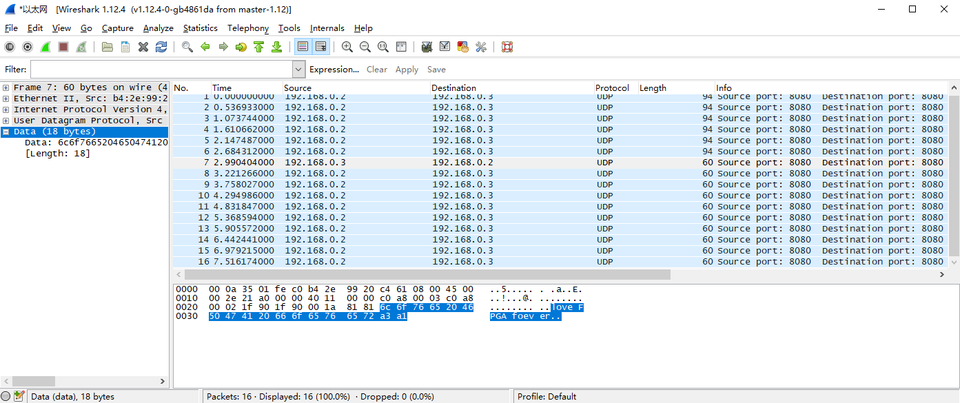
Figure 14. 20 PC send data package

Figure 14.21 The FPGA repackages the received data and sends it to the PC
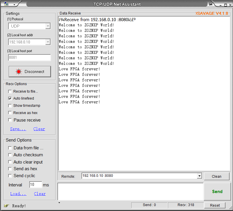
Figure 14.22 Information received by PC from FPGA
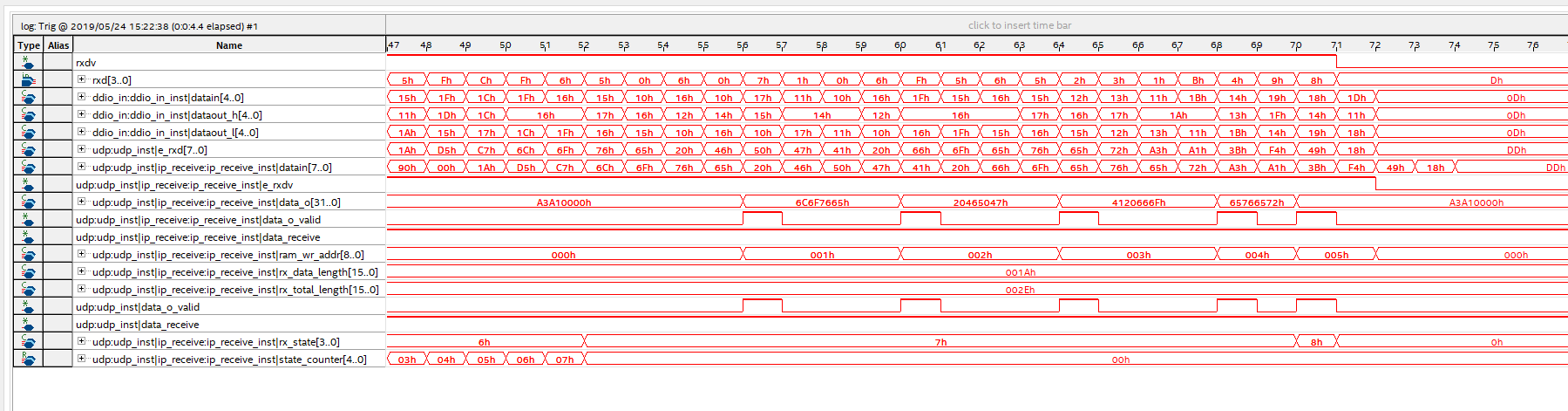
Figure 14.23 FPGA end data and stored in the RAM process
It should be noted that Ethernet II specifies the Ethernet frame data field is a minimum of 46 bytes, that is, the minimum Ethernet frame is 6+6+2+46+4=64. The 4-byte FCS is removed, so the packet capture is 60 bytes. When the length of the data field is less than 46 bytes, the MAC sublayer is padded after the data field to satisfy the data frame length of not less than 64 bytes. When communicating over a UDP LAN, “Hello World” often occurs for testing, but “Hello World” does not meet the minimum valid data (64-46) requirements. It is less than 18 bytes but the other party is still available for receiving, because data is complemented in the MAC sublayer of the link layer, less than 18 bytes are padded with ‘0’s. However, when the server is on the public network and the client is on the internal network, if less than 18 bytes of data is transmitted, the receiving end cannot receive the data. Therefore, if there is no data received, the information to be sent should be increased to more than 18 bytes.
Experiment 15 SRAM Read and Write
15.1 Experiment Objective
- Learn the read and write of SRAM
- Review frequency division, button debounce, and hex conversion experiment content
15.2 Experiment Implement
- Control the read and write function of SRAM by controlling the button
- The data written to the SRAM is read out again and displayed on the segment display
- In the process of reading data, it is required to have a certain time interval for each read operation.
15.3 Experiment
15.3.1 Introduction to SRAM
SRAM (Static Random-Access Memory) is a type of random access memory. The “static” means that as long as the power is on, the data in the SRAM will remain unchanged. However, the data will still be lost after power turned off, which is the characteristics of the RAM.
Two SRAMs (IS61WV25616BLL) are on the development board, each SRAM has 256 * 16 words of storage space. Each word is 16-bit. The maximum read and write speed can reach 100 MHz. The physical picture is shown in Figure 15.1.
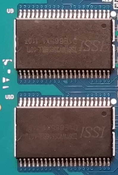
Figure 15.1 SRAM physical picture
15.3.2 Hardware Design
As shown in Figure 15.2, a set of control signals (low signal is valid): chip selection signal CE, read control signal OE, write enable control number WE, and two byte control signals UB and LB, through CE_N_SRAM, OE_N_SRAM, WE_N_SRAM, UB_N_SRAM, LB_N_SRAM, connect to the FPGA, and the read and write status is controlled by the FPGA. The address is sent to the SRAM through the address line A[17:0]. In the write state, the data to be written is sent to the SRAM through the data line D[15:0], and can be written into the register of the corresponding address; In the read state, the data in the corresponding address register can be directly read into the FPGA by the data line.
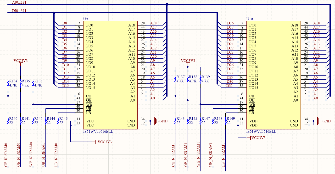
Figure 15.2 Schematics of SRAM
15.3.3 Introduction to the Program
This experiment will use the frequency division, button debounce, hex conversion and segment display module. (Refer to the previous experiment for more information) Here SRAM read and write module is mainly introduced.
The first step: the establishment of the main program framework
|
The inputs are 50 MHz system clock IN_CLK_50M, button module PB[7:1], PB[3] (RETURN) as external hardware reset, PB[2] (UP) as write control, PB[7] (DOWN) as read control. The output has two sets of control signals to control two srams respectively, specifically chip selection signal sram_cs_n, write control signal sram_we_n, read control signal sram_oe_n, and byte control signals sram_ub_n and sram_lb_n, address bus sram_daddr[17:0], data bus Sram_data[31:0], and the segment display bit selection signal tube_sel[5:0] and the segment selection signal tube_seg[7:0].
The second step: SRAM read and write module
In this experiment, two SRAMs are used simultaneously and are expanded into a 32-bit wide data memory.
|
In the write state, the write enable wr_en is pulled high. At this time, sram_data is the data wr_data to be written. In other cases, the write enable is pulled low. In the read state, the data is directly read into the FPGA by sram_data.
At reset, the SRAM control signals are all pulled high, then jumps to the 0 state, and the data is read and written by the state machine.
0 state: an initial address “511” is given, and an initial data “123456”, when the write enable signal PB_flag[2] is valid, the chip selection signal pulls down the selected SRAM. The write control signal is pulled low to prepare for write operation, and the read control signal remains pulled up. Meanwhile, the byte control signal is pulled low, indicating that the high and low two bytes of data are simultaneously written and then jump to the 1 state. When the read enable signal PB_flag[7] is active, in contrast to the write enable, the write control signal is held high, the read control signal is pulled low to prepare for the read operation, and jumps to the 2 state.
1 state: starting from the initial address “511”, writing initial data “123456”, each clock cycle address and data are simultaneously decremented by one, performing 512 data continuous write operations. When the register address bit is ‘0’, end the write operation and jum to the 4 state.
2 state: Starting from the initial address “511”, the address is decremented by 1 every 1 second under the control of the second pulse s_flag, and a continuous read operation of 512 data is performed. When the data is completely read, the address jumps to the 4 state when the address is ‘0’.
4 state: The control signals are all pulled high, deactivate the control of the SRAM, jumping to the ‘0’ state, an waiting for the next operation.
15.4 Experiment Verification
The first step: pin assignment
Table 15.1 SRAM read and write experiment pin mapping
The second step: board verification
After the pin assignment is completed, the compilation is performed, and the board is verified after passing.
After the development board is programmed, the segment display will all light up, but because no data is read, the segment display will display all ‘0’s, as shown in Figure 15.3. Press the PB[2] (UP) button to write the data to the SRAM, and then press the PB[7] (DOWN) button to read the written data. At this time, it displays “123456” and decrement by one every second. See Figure 15.4. From this it is verified that the specified data is written into the SRAM and is read correctly.
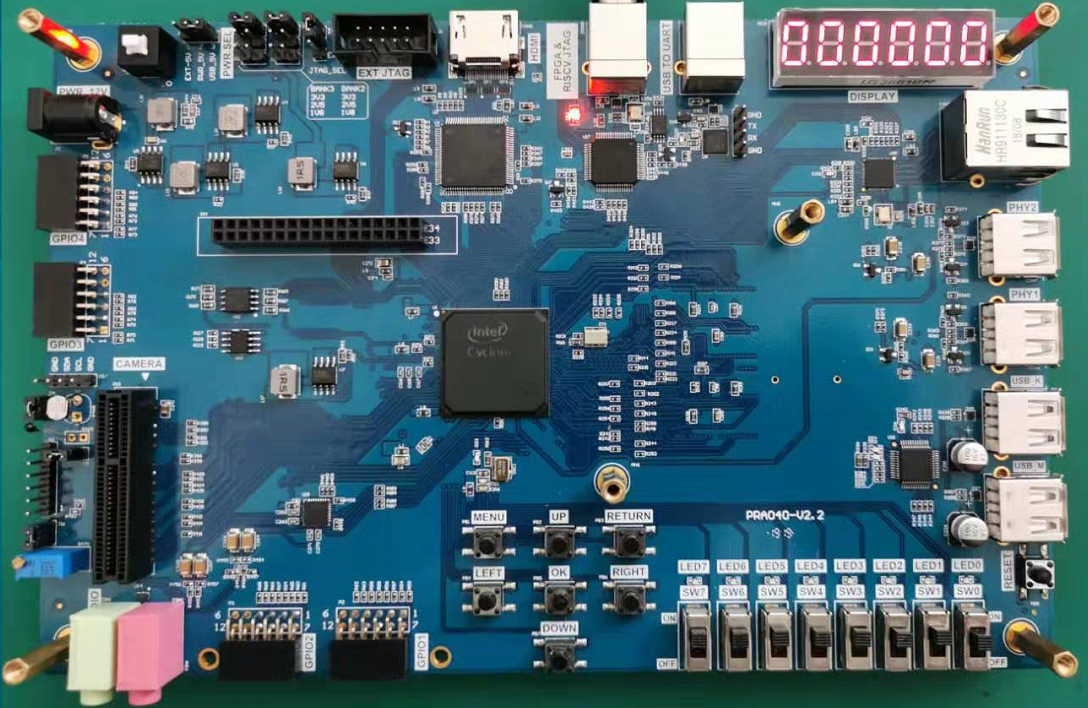
Figure 15.3 SRAM write and read 1
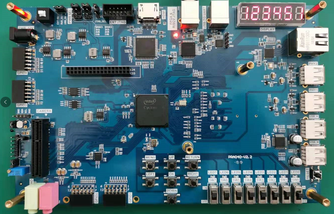
Figure 15.4 SRAM write and read 2
Experiment 16 8978 Audio Loopback Experiment
16.1 Experiment Objective
- Learn about I2S (Inter-IC Sound) bus and how it works
- Familiar with the working mode of WM8978. And by configuring the interface mode and selecting the relevant registers in combination with the development board, complete the data transmission and reception, and verify it
16.2 Experiment Implement
- Perform audio loopback test by configuring the onboard audio chip WM8978 to check if the hardware is working properly
- Adjust the volume output level with the keys.
16.3 Experiment
16.3.1 WM8978 Introduction
WM8978 is a low power, high quality stereo multimedia digital signal CODEC introduced by Wolfson. It is mainly used in portable applications such as digital cameras and camcorders. Advanced on-chip digital signal processing includes a 5-band equaliser, a mixed signal Automatic Level Control for the microphone or line input through the ADC as well as a purely digital limiter function for record or playback. Additional digital filtering options are available in the ADC path, to cater for application filtering, such as “wind noise reduction”.
See Figure 16.1 for the internal structure block diagram of WM8978.
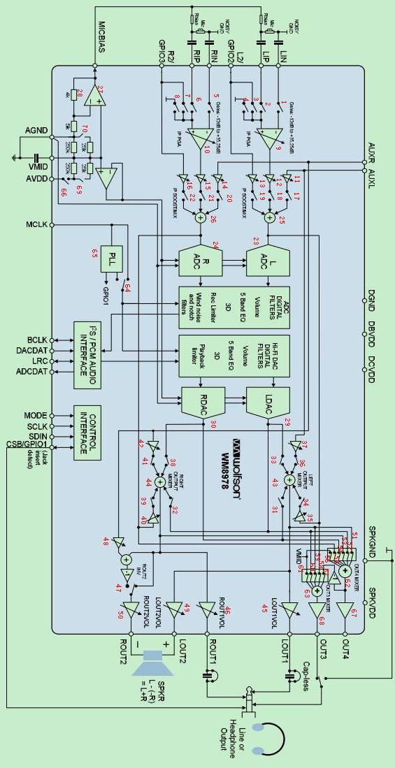
Figure 16.1 WM8978 internal structure block diagram
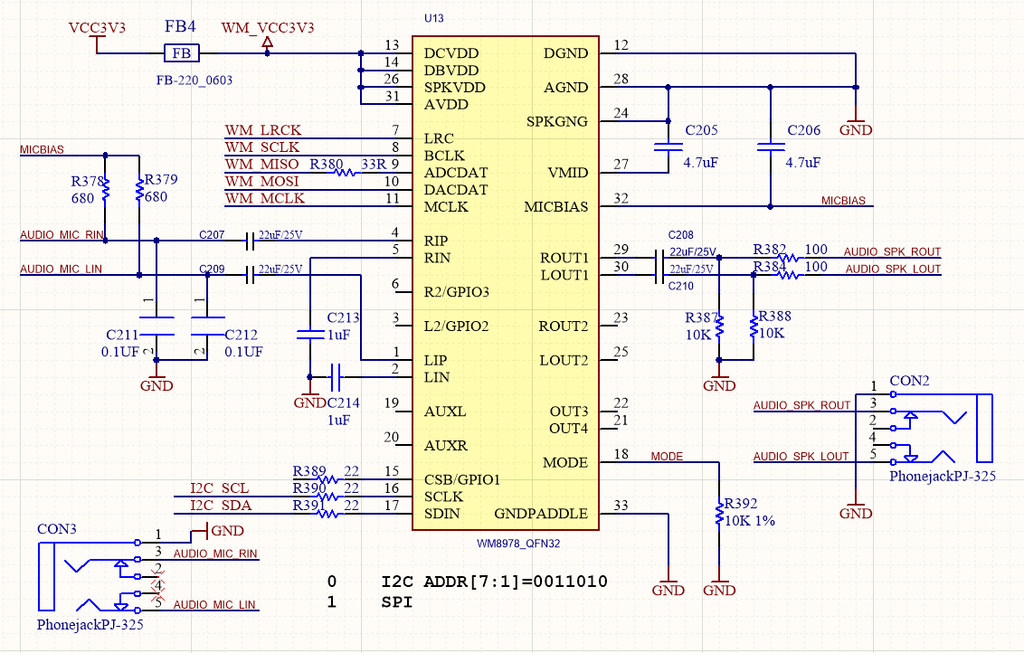
Figure 16.2 Schematics of the audio part of the development board
16.3.2 WM8978 Control Interface Timing
The WM8978 control interface has two-wire mode and three-wire mode. The specific mode is selected by the MODE pin connection of WM8978. When the mode pin is connected to a low voltage level, it is a two-wire mode, and when it is connected to a high voltage level, it is a three-wire mode. The development board mode pin is grounded. When the control interface is in two-wire mode, the timing diagram is shown in Figure 16.3. The timing diagram is the same as the IIC timing. The device address of WM8978 is fixed to 7’b0011010. This chip register only supports writing and does not support reading.
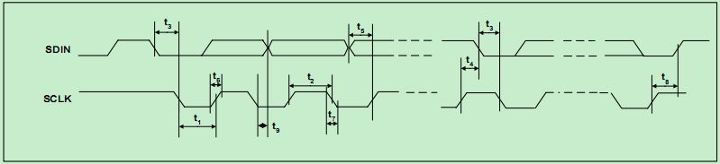
Figure 16.3 Timing diagram of the two-wire mode interface
16.3.3 I2S Audio Bus Protocol
I2S (Inter-IC Sound Bus) is just a branch of PCM, the interface definition is the same, I2S sampling frequency is generally 44.1KHz and 48KHz, PCM sampling frequency is generally 8K, 16K. There are four groups of signals: bit clock signal, synchronization signal, data input, data output.
I2S is a bus standard developed by Philips for audio data transmission between digital audio devices. In the Philips I2S standard, both the hardware interface specification and the format of digital audio data are specified. I2S has three main signals: the serial clock SCLK, also known as the bit clock BCLK, which corresponds to each bit of data of digital audio. The frequency of SCLK = 2 × sampling frequency × sampling number of bits. The frame clock LRCK is used to switch the data of the left and right channels. An LRCK of “0” indicates that data of the left channel is being transmitted, and “1” indicates that data of the right channel is being transmitted. LRCLK == FS, is the sampling frequency serial data SDATA, which is audio data expressed in two’s complement. Sometimes in order to enable better synchronization between systems, another signal MCLK is needed, which is called the master clock, or also called the system Clock (System Clock). It is 256 or 384 times the sampling frequency.
The timing of the I2S protocol is shown in Figure 16.4. However many bits of data the I2S format signal has, the most significant bit of the data always appears at the second BCLK pulse after the LRCK change (that is, the beginning of a frame). This allows the number of significant digits at the receiving end and the transmitting end to be different. If the receiving end can process less significant bits than the transmitting end, the extra low-order data in the data frame can be discarded; if the receiving end can process more significant bits than the transmitting end, it can make up the remaining bits by itself. This synchronization mechanism makes the interconnection of digital audio equipment more convenient without causing data errors.
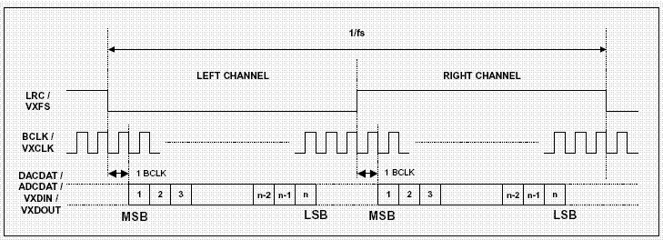
Figure 16.4 I2S timing protocol
16.3.4 Main Program Design
- WM8978 register configuration program
Only the program of register configuration program is given here, please refer to the project file for the complete program
| module wm8978_config
( input clk_50m, output reg cfg_done=0, input rst_n, input rxd, output txd, input key1, input key2, output i2c_sclk, inout i2c_sdat ); wire tr_end; reg [4:0] i; //************************************ reg [23:0] i2c_data_r=0; wire [7:0] data_read ; reg [7:0] read_req ; reg uart_rd =0; reg uart_wr =0; reg [7:0] txd_i2c_data; reg txd_start = 0; wire txd_busy; wire [7:0] rxd_i2c_data; wire rxd_ready; wire rxd_eop; wire test_pin; uart_transceiver uart_transceiver_inst ( .sys_clk (clk_50m), // 50m .uart_rx (rxd), .uart_tx (txd), .divisor (55), // 115200 * 8 .rx_data (rxd_i2c_data), .rx_done (rxd_ready), .rx_eop (rxd_eop), .tx_data (txd_i2c_data), .tx_wr (txd_start), .tx_done (), .tx_busy (txd_busy), .test_pin (), .sys_rst () ); reg rx_end_ack = 0; reg rx_end = 0; always @ (posedge clk_50m) if(rxd_eop) rx_end <= 1; else if(rx_end_ack) rx_end <= 0; reg [7:0] cmd_dir = 0; reg [3:0] uart_st = 0; always @ (posedge clk_50m) if(cfg_done == 0) begin rx_end_ack <= 0; uart_wr <= 0; uart_rd <= 0; uart_st <= 0; end else case(uart_st) 0: begin rx_end_ack <= 0; uart_wr <= 0; uart_rd <= 0; if(rxd_ready) begin cmd_dir <= rxd_i2c_data; uart_st <= 1; end end 1: begin if(rxd_ready) begin i2c_data_r[23:16] <= rxd_i2c_data; uart_st <= 2; end end 2: begin if(rxd_ready) begin i2c_data_r[15:08] <= rxd_i2c_data; if(cmd_dir[0]) uart_st <= 5; else uart_st <= 3; end end 3: // write begin if(rxd_ready) begin i2c_data_r[07:00] <= rxd_i2c_data; uart_wr <= 1; uart_st <= 4; end end 4: begin if(tr_end) begin uart_wr <= 0; uart_st <= 7; end end 5: //read begin uart_rd <= 1; uart_st <= 6; end 6: begin uart_rd <= 0; if(tr_end) begin txd_i2c_data <= data_read; txd_start <= 1; uart_st <= 7; end end 7: begin txd_start <= 0; if(rx_end) begin rx_end_ack <= 1; uart_st <= 0; end else rx_end_ack <= 0; end endcase //*************************************** reg start; //parameter define reg [5:0] PHONE_VOLUME = 6’d32; reg [5:0] SPEAK_VOLUME = 6’d32; reg [31:0] i2c_data=0 ; reg [7:0] start_init_cnt; reg [4:0] init_reg_cnt ; reg [25:0] on_counter; reg [25:0] off_counter; reg key_up, key_down; always @(posedge clk_50m , negedge cfg_done) if (!cfg_done) begin on_counter<=0; off_counter<=0; key_up<=1’b0; key_down<=1’b0; end else begin if (key1==1’b1) on_counter<=0; else if ((key1==1’b0)& (on_counter<=500000)) on_counter<=on_counter+1’b1; if (on_counter==49950) key_up<=1’b1; else key_up<=1’b0; if (key2==1’b1) off_counter<=0; else if ((key2==1’b0)& (off_counter<=500000)) off_counter<=off_counter+1’b1; if (off_counter==49950) key_down<=1’b1; else key_down<=1’b0; end always @(posedge clk_50m , negedge cfg_done) if (!cfg_done) begin PHONE_VOLUME <=6’d32 ; end else begin if (( 2<=PHONE_VOLUME )&( PHONE_VOLUME <=56)&(on_counter==49948)) PHONE_VOLUME <=PHONE_VOLUME+6 ; else if (( 8<=SPEAK_VOLUME )&( SPEAK_VOLUME <=62)& (off_counter==49948)) PHONE_VOLUME <=PHONE_VOLUME-6 ; else PHONE_VOLUME <=PHONE_VOLUME ; end always @ ( posedge clk_50m ) if( rst_n==1’b0 ) begin i <= 5’d0; read_req<=0 ; i2c_data <= 32’h000000; start <= 1’b0; cfg_done <=0; end else begin case( i ) 0: begin if( tr_end ) begin start <= 1’b00; i <= i + 1’b1; end else begin start <= 1’b1; i2c_data <= {7’h1a,1’b0,8’h00,7’d0 ,9’b1}; end end 1: begin if( tr_end ) begin start <= 1’b0; i <= i + 1’b1; end else begin start <= 1’b1; i2c_data <={7’h1a,1’b0, 8’h00,7’d1 ,9’b1_0010_1111}; end end 2: begin if( tr_end ) begin start <= 1’b0; i <= i + 1’b1; end else begin start <= 1’b1; i2c_data <= {7’h1a,1’b0,8’h00,7’d2 ,9’b1_1011_0011}; end end 3: begin if( tr_end ) begin start <= 1’b0; i <= i + 1’b1; end else begin start <= 1’b1; i2c_data <= {7’h1a,1’b0,8’h00,7’d3 ,9’b0_0110_1111}; end end 4: begin if( tr_end ) begin start <= 1’b0; i <= i + 1’b1; end else begin start <= 1’b1; i2c_data <= {7’h1a,1’b0,8’h00,7’d4 ,{2’d0,2’b11,5’b10000}}; end end 5: begin if( tr_end ) begin start <= 1’b0; i <= i + 1’b1; end else begin start <= 1’b1; i2c_data <={7’h1a,1’b0,8’h00,7’d6 ,9’b0_0000_0001}; end end 6: begin if( tr_end ) begin start <= 2’b00; i <= i + 1’b1; end else begin start <= 1’b1; i2c_data<= {7’h1a,1’b0,8’h00,7’d7 ,9’b0_0000_0001}; end end 7: begin if( tr_end ) begin start <= 1’b0; i <= i + 1’b1; end else begin start <= 1’b1; i2c_data <= {7’h1a,1’b0,8’h00,7’d10,9’b0_0000_1000}; end end 8: begin if( tr_end ) begin start <= 1’b0; i <= i + 1’b1; end else begin start <= 1’b1; i2c_data <= {7’h1a,1’b0,8’h00,7’d14,9’b1_0000_1000}; end end 9: begin if( tr_end ) begin start <= 1’b0; i <= i + 1’b1; end else begin start <= 1’b1; i2c_data <= {7’h1a,1’b0,8’h00,7’d43,9’b0_0001_0000}; end end 10: begin if( tr_end ) begin start <= 1’b0; i <= i + 1’b1; end else begin start <= 1’b1; i2c_data <={7’h1a,1’b0,8’h00,7’d47,9’b0_0111_0000}; end end 11: begin if( tr_end ) begin start <= 1’b0; i <= i + 1’b1; end else begin start <= 1’b1; i2c_data <={7’h1a,1’b0,8’h00,7’d48,9’b0_0111_0000}; end end 12: begin if( tr_end ) begin start <= 1’b0; i <= i + 1’b1; end else begin start <= 1’b1; i2c_data <={7’h1a,1’b0,8’h00,7’d49,9’b0_0000_0110}; end end 13: begin if( tr_end ) begin start <= 1’b0; i <= i + 1’b1; end else begin start <= 1’b1; i2c_data <= {7’h1a,1’b0,8’h00,7’d50,9’b1 };end end 14: begin if( tr_end ) begin start <= 1’b0; i <= i + 1’b1; end else begin start <= 1’b1; i2c_data <= {7’h1a,1’b0,8’h00,7’d51,9’b1 };end end 15: begin if( tr_end ) begin start <= 1’b0; i <= i + 1’b1; end else begin start <= 1’b1; i2c_data <={7’h1a,1’b0,8’h00,7’d52,{3’b010,PHONE_VOLUME}};end end 16: begin if( tr_end ) begin start <= 1’b0; i <= i + 1; end else begin start <= 1’b1; i2c_data <= {7’h1a,1’b0,8’h00,7’d53,{3’b110,PHONE_VOLUME}};end end 17: begin cfg_done<=1 ; if (uart_wr) begin start <= 1’b1; i2c_data <={cmd_dir,i2c_data_r} ; i<=i+1 ; end if (uart_rd) begin read_req <= 1’b1; i2c_data <={cmd_dir,i2c_data_r} ; i<=i+2 ; end if (key_up|key_down) i<= 15; end 18: begin if( tr_end ) begin start <= 1’b0; i <=19; end else i<=20; end 19: begin if( tr_end ) begin read_req <= 1’b0; i <= 19; end else begin i<=21;end end default:i<=1 ; endcase end i2c_control i2c_control_inst ( .Clk (clk_50m), .Rst_n(rst_n), .wrreg_req(start) , .rdreg_req (read_req), .addr({i2c_data[15:8],i2c_data[23:16]}) , //16bit .addr_mode(0), .wrdata (i2c_data[7:0]), // .rddata (data_read), //8bit .device_id (i2c_data[31:24]), //8bit .RW_Done(tr_end), .ack (), .i2c_sclk(i2c_sclk), .i2c_sdat(i2c_sdat) ); endmodule |
- Audio signal acquisition program
| module audio_receive (
//system clock 50MHz input rst_n , //wm8978 interface input aud_bclk , input aud_lrc , input aud_adcdat, //user interface output reg rx_done , output reg [31:0] adc_data ); parameter WL = 6’d32 ; reg aud_lrc_d0; reg [ 5:0] rx_cnt; reg [31:0] adc_data_t; wire lrc_edge ; assign lrc_edge = aud_lrc ^ aud_lrc_d0; always @(posedge aud_bclk or negedge rst_n) begin if(!rst_n) aud_lrc_d0 <= 1’b0; else aud_lrc_d0 <= aud_lrc; end always @(posedge aud_bclk or negedge rst_n) begin if(!rst_n) begin rx_cnt <= 6’d0; end else if(lrc_edge == 1’b1) rx_cnt <= 6’d0; else if(rx_cnt < 6’d35) rx_cnt <= rx_cnt + 1’b1; end always @(posedge aud_bclk or negedge rst_n) begin if(!rst_n) begin adc_data_t <= 32’b0; end else if(rx_cnt < WL) adc_data_t[WL – 1’d1 – rx_cnt] <= aud_adcdat; always @(posedge aud_bclk or negedge rst_n) begin if(!rst_n) begin rx_done <= 1’b0; adc_data <= 32’b0; end else if(rx_cnt == 6’d32) begin rx_done <= 1’b1; adc_data<= adc_data_t; end else rx_done <= 1’b0; end endmodule |
- Audio sending module
| module audio_send (
input rst_n , input aud_bclk , input aud_lrc , output reg aud_dacdat, input [31:0] dac_data , output reg tx_done ); parameter WL = 6’d32 ; reg aud_lrc_d0; reg [ 5:0] tx_cnt; reg [31:0] dac_data_t; wire lrc_edge; assign lrc_edge = aud_lrc ^ aud_lrc_d0; always @(posedge aud_bclk or negedge rst_n) begin if(!rst_n) aud_lrc_d0 <= 1’b0; else aud_lrc_d0 <= aud_lrc; end always @(posedge aud_bclk or negedge rst_n) begin if(!rst_n) begin tx_cnt <= 6’d0; dac_data_t <= 32’d0; end else if(lrc_edge == 1’b1) begin tx_cnt <= 6’d0; dac_data_t <= dac_data; end else if(tx_cnt < 6’d35) tx_cnt <= tx_cnt + 1’b1; end always @(posedge aud_bclk or negedge rst_n) begin if(!rst_n) begin tx_done <= 1’b0; end else if(tx_cnt == 6’d32) tx_done <= 1’b1; else tx_done <= 1’b0; end always @(negedge aud_bclk or negedge rst_n) begin if(!rst_n) begin aud_dacdat <= 1’b0; end else if(tx_cnt < WL) aud_dacdat <= dac_data_t[WL – 1’d1 – tx_cnt]; else aud_dacdat <= 1’b0; end endmodule |
- Main program
| module audio_test(
input wire sys_clk_50, input wire rst_n, input rxd, output txd, output [7:0] led , input key1, input key2, inout wm_sdin, output wm_sclk, input wire wm_lrc, input wire wm_bclk, input wire adcdat, output wire dacdat, output wire mclk ); wire cfg_done ; assign led ={7’h7f,~cfg_done} ; pll_50_12 pll_50_12_inst ( // Clock out ports .c0(clk_out_12), // output clk_out_12 // Status and control signals .areset(~rst_n), // input reset .locked(locked), // output locked // Clock in ports .inclk0(sys_clk_50)); // input sys_clk_50 wire clk_out_12 ; assign mclk = clk_out_12 ; wm8978_config wm8978_config_inst ( .key1 (key1), .key2 (key2), .clk_50m (sys_clk_50 ) , .rst_n (rst_n) , .cfg_done (cfg_done) , .i2c_sclk (wm_sclk) , .rxd (rxd), .txd (txd), .i2c_sdat (wm_sdin) ); wire [31:0] adc_data ; audio_receive audio_receive_inst( .rst_n (rst_n), .aud_bclk (wm_bclk), .aud_lrc (wm_lrc), .aud_adcdat (adcdat), .adc_data (adc_data), .rx_done (rx_done) ); audio_send audio_send_inst( .rst_n (rst_n), .aud_bclk (wm_bclk), .aud_lrc (wm_lrc), .aud_dacdat (dacdat), .dac_data (adc_data), .tx_done (tx_done) ); endmodule |
16.4 Experiment Verification
- Pin assignment
Table 16.1 Pin assignment
| Signal Name | Port Description | Network Label | FPGA Pin |
| Sys_clk_50 | System 50M clock | C10_50MCLK | G21 |
| Reset_n | System reset signal | KEY1 | Y4 |
| Wm_sdin | 8978 register configuration data line | I2C_SDA | C13 |
| Wm_sclk | 8978 register configuration clock | I2C_SCL | D13 |
| Wm_lrc | 8978 align clock | WM_LRCK | AB19 |
| Wm_bclk | 8978 bit clock | WM_BCLK | AA19 |
| adcdat | ADC input of 8978 | WM_MISO | AA18 |
| Dacdat | DAC input of 8978 | WM_MOSI | Y17 |
| Mack | PLL provides 8978 working master clock | WM_MCLK | W17 |
| Key1 | Volume up button | Key2 | V5 |
| Key2 | Volume down button | Key7 | AB3 |
| txd | Serial transmit | TTL_RX | E16 |
| rxd | Serial receive | TTL_TX | F15 |
- Board verification
As shown in Figure 16.5 below, after the FPGA development board is programmed, use a dual male audio cable, with one end plugged into the red audio receiver end and the other end plugged into a music player. Plug the headphone into the green audio playback port. The music can be heard from player. The volume is divided into 5 gears. Press the UP key to increase the volume and press the down key to decrease the volume.
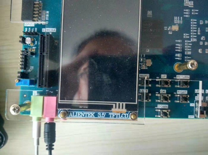
Figure 16.5 wm8978 board verification
Experiment 17 Photo Display Experiment of OV5640 Camera
17.1 Experiment Objective
Understand the power-on sequence of the OV5640 camera and the corresponding register configuration process when outputting images of different resolutions- Review previous knowledge of IIC bus
- Review previous knowledge of HDMI
17.2 Experiment Implement
Read the power-on sequence of the OV5640 datasheet, and correctly write the power-on control program according to the peripheral module schematics.- Correctly write the configuration program of the OV5640 camera with a resolution of 640X480 according to the timing requirements of the SCCB interface
- Based on previous experiments, write a program to store the image data collected by 5640 in the development board SRAM.
- Write a program to display the image stored in the SRAM to the monitor via HDMI.
- The refresh of the image is controlled by the keys, and the screen display image is updated every time pressing it, similar to a camera.
17.3 Experiment
Some main procedures are given below. Refer the project file for the complete program
- Ov5640 power-on initialization program design is based on the power-on timing diagram of 5640 when connected to DVDD. Shown in Figure 17.1.
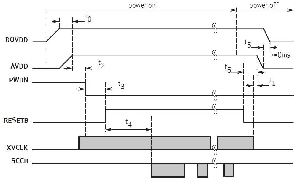
Figure 17.1 5640 power-on sequence
Power-on sequence program is as follows:
| module power_on_delay(clk_50M,reset_n_r,camera_pwup,initial_en,cam_resetb);
input clk_50M; input reset_n_r; output camera_pwup; output initial_en; (*mark_debug=”true”*)output reg cam_resetb =0; (*mark_debug=”true”*)reg [31:0]cnt1=0; reg initial_en=0; reg camera_pwup_reg=0; reg reset_n =0; assign camera_pwup=camera_pwup_reg; always @ (posedge clk_50M) reset_n<=reset_n_r ; //5ms, delay from sensor power up stable to Pwdn pull down always@(posedge clk_50M) begin if(reset_n==1’b0) cnt1<=0; else begin if (cnt1<50000000) cnt1<=cnt1+1 ; else cnt1<=cnt1 ; end end always@(posedge clk_50M) begin if(reset_n==1’b0) begin camera_pwup_reg<=0; end else begin if (cnt1==15000000) camera_pwup_reg<=1; else camera_pwup_reg<=camera_pwup_reg; end end always@(posedge clk_50M) begin if(reset_n==1’b0) begin cam_resetb <=0; end else begin if (cnt1==35000000) cam_resetb <=1; else cam_resetb <=cam_resetb ; end end always@(posedge clk_50M) begin if(reset_n==1’b0) begin initial_en<=0; end else begin if (cnt1==48000000) initial_en<=1; else initial_en<=initial_en; end end endmodule |
- 5640 chip configuration program
After the development board is powered on correctly, the OV5640 related registers will be configured. The configuration of the OV5640 chip’s internal registers is performed through the SCCB (Serial Camera Control Bus) protocol. This protocol is equivalent to a simple I2C bus. The SCCB timing is shown in Figure 17.2. When configuring, use the I2C code from previous experiment directly.
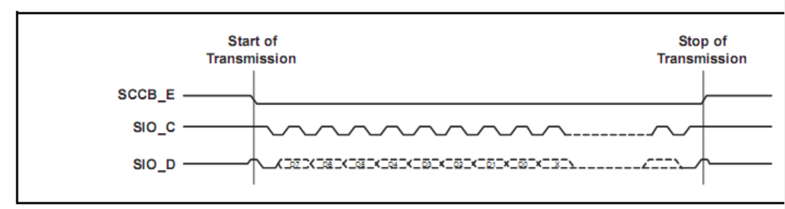
Figure 17.2 SCCB write register timing diagram
The registers required to complete the 5640 camera function are as follows:
| always@(reg_index)
begin case(reg_index) 0:reg_data<=24’h310311; 1:reg_data<=24’h300882; 2:reg_data<=24’h300842; 3:reg_data<=24’h310303; 4:reg_data<=24’h3017ff; 5:reg_data<=24’h3018ff; 6:reg_data<=24’h30341A; 7:reg_data<=24’h303713; 8:reg_data<=24’h310801; 9:reg_data<=24’h363036; 10:reg_data<=24’h36310e; 11:reg_data<=24’h3632e2; 12:reg_data<=24’h363312; 13:reg_data<=24’h3621e0; 14:reg_data<=24’h3704a0; 15:reg_data<=24’h37035a; 16:reg_data<=24’h371578; 17:reg_data<=24’h371701; 18:reg_data<=24’h370b60; 19:reg_data<=24’h37051a; 20:reg_data<=24’h390502; 21:reg_data<=24’h390610; 22:reg_data<=24’h39010a; 23:reg_data<=24’h373112; 24:reg_data<=24’h360008; 25:reg_data<=24’h360133; 26:reg_data<=24’h302d60; 27:reg_data<=24’h362052; 28:reg_data<=24’h371b20; 29:reg_data<=24’h471c50; 30:reg_data<=24’h3a1343; 31:reg_data<=24’h3a1800; 32:reg_data<=24’h3a19f8; 33:reg_data<=24’h363513; 34:reg_data<=24’h363603; 35:reg_data<=24’h363440; 36:reg_data<=24’h362201; 37:reg_data<=24’h3c0134; 38:reg_data<=24’h3c0428; 39:reg_data<=24’h3c0598; 40:reg_data<=24’h3c0600; 41:reg_data<=24’h3c0708; 42:reg_data<=24’h3c0800; 43:reg_data<=24’h3c091c; 44:reg_data<=24’h3c0a9c; 45:reg_data<=24’h3c0b40; 46:reg_data<=24’h381000; 47:reg_data<=24’h381110; 48:reg_data<=24’h381200; 49:reg_data<=24’h370864; 50:reg_data<=24’h400102; 51:reg_data<=24’h40051a; 52:reg_data<=24’h300000; 53:reg_data<=24’h3004ff; 54:reg_data<=24’h300e58; 55:reg_data<=24’h302e00; 56:reg_data<=24’h430061; 57:reg_data<=24’h501f01; 58:reg_data<=24’h440e00; 59:reg_data<=24’h5000a7; 60:reg_data<=24’h3a0f30; 61:reg_data<=24’h3a1028; 62:reg_data<=24’h3a1b30; 63:reg_data<=24’h3a1e26; 64:reg_data<=24’h3a1160; 65:reg_data<=24’h3a1f14; 66:reg_data<=24’h580023; 67:reg_data<=24’h580114; 68:reg_data<=24’h58020f; 69:reg_data<=24’h58030f; 70:reg_data<=24’h580412; 71:reg_data<=24’h580526; 72:reg_data<=24’h58060c; 73:reg_data<=24’h580708; 74:reg_data<=24’h580805; 75:reg_data<=24’h580905; 76:reg_data<=24’h580a08; 77:reg_data<=24’h580b0d; 78:reg_data<=24’h580c08; 79:reg_data<=24’h580d03; 80:reg_data<=24’h580e00; 81:reg_data<=24’h580f00; 82:reg_data<=24’h581003; 83:reg_data<=24’h581109; 84:reg_data<=24’h581207; 85:reg_data<=24’h581303; 86:reg_data<=24’h581400; 87:reg_data<=24’h581501; 88:reg_data<=24’h581603; 89:reg_data<=24’h581708; 90:reg_data<=24’h58180d; 91:reg_data<=24’h581908; 92:reg_data<=24’h581a05; 93:reg_data<=24’h581b06; 94:reg_data<=24’h581c08; 95:reg_data<=24’h581d0e; 96:reg_data<=24’h581e29; 97:reg_data<=24’h581f17; 98:reg_data<=24’h582011; 99:reg_data<=24’h582111; 100:reg_data<=24’h582215; 101:reg_data<=24’h582328; 102:reg_data<=24’h582446; 103:reg_data<=24’h582526; 104:reg_data<=24’h582608; 105:reg_data<=24’h582726; 106:reg_data<=24’h582864; 107:reg_data<=24’h582926; 108:reg_data<=24’h582a24; 109:reg_data<=24’h582b22; 110:reg_data<=24’h582c24; 111:reg_data<=24’h582d24; 112:reg_data<=24’h582e06; 113:reg_data<=24’h582f22; 114:reg_data<=24’h583040; 115:reg_data<=24’h583142; 116:reg_data<=24’h583224; 117:reg_data<=24’h583326; 118:reg_data<=24’h583424; 119:reg_data<=24’h583522; 120:reg_data<=24’h583622; 121:reg_data<=24’h583726; 122:reg_data<=24’h583844; 123:reg_data<=24’h583924; 124:reg_data<=24’h583a26; 125:reg_data<=24’h583b28; 126:reg_data<=24’h583c42; 127:reg_data<=24’h583dce; 128:reg_data<=24’h5180ff; 129:reg_data<=24’h5181f2; 130:reg_data<=24’h518200; 131:reg_data<=24’h518314; 132:reg_data<=24’h518425; 133:reg_data<=24’h518524; 134:reg_data<=24’h518609; 135:reg_data<=24’h518709; 136:reg_data<=24’h518809; 137:reg_data<=24’h518975; 138:reg_data<=24’h518a54; 139:reg_data<=24’h518be0; 140:reg_data<=24’h518cb2; 141:reg_data<=24’h518d42; 142:reg_data<=24’h518e3d; 143:reg_data<=24’h518f56; 144:reg_data<=24’h519046; 145:reg_data<=24’h5191f8; 146:reg_data<=24’h519204; 147:reg_data<=24’h519370; 148:reg_data<=24’h5194f0; 149:reg_data<=24’h5195f0; 150:reg_data<=24’h519603; 151:reg_data<=24’h519701; 152:reg_data<=24’h519804; 153:reg_data<=24’h519912; 154:reg_data<=24’h519a04; 155:reg_data<=24’h519b00; 156:reg_data<=24’h519c06; 157:reg_data<=24’h519d82; 158:reg_data<=24’h519e38; 159:reg_data<=24’h548001; 160:reg_data<=24’h548108; 161:reg_data<=24’h548214; 162:reg_data<=24’h548328; 163:reg_data<=24’h548451; 164:reg_data<=24’h548565; 165:reg_data<=24’h548671; 166:reg_data<=24’h54877d; 167:reg_data<=24’h548887; 168:reg_data<=24’h548991; 169:reg_data<=24’h548a9a; 170:reg_data<=24’h548baa; 171:reg_data<=24’h548cb8; 172:reg_data<=24’h548dcd; 173:reg_data<=24’h548edd; 174:reg_data<=24’h548fea; 175:reg_data<=24’h54901d; 176:reg_data<=24’h53811e; 177:reg_data<=24’h53825b; 178:reg_data<=24’h538308; 179:reg_data<=24’h53840a; 180:reg_data<=24’h53857e; 181:reg_data<=24’h538688; 182:reg_data<=24’h53877c; 183:reg_data<=24’h53886c; 184:reg_data<=24’h538910; 185:reg_data<=24’h538a01; 186:reg_data<=24’h538b98; 187:reg_data<=24’h558006; 188:reg_data<=24’h558340; 189:reg_data<=24’h558410; 190:reg_data<=24’h558910; 191:reg_data<=24’h558a00; 192:reg_data<=24’h558bf8; 193:reg_data<=24’h501d40; 194:reg_data<=24’h530008; 195:reg_data<=24’h530130; 196:reg_data<=24’h530210; 197:reg_data<=24’h530300; 198:reg_data<=24’h530408; 199:reg_data<=24’h530530; 200:reg_data<=24’h530608; 201:reg_data<=24’h530716; 202:reg_data<=24’h530908; 203:reg_data<=24’h530a30; 204:reg_data<=24’h530b04; 205:reg_data<=24’h530c06; 206:reg_data<=24’h502500; 207:reg_data<=24’h300802; //680×480 30帧/秒, night mode 5fps, input clock =24Mhz, PCLK =56Mhz 208:reg_data<=24’h303511; 209:reg_data<=24’h303646; 210:reg_data<=24’h3c0708; 211:reg_data<=24’h382047; 212:reg_data<=24’h382101; 213:reg_data<=24’h381431; 214:reg_data<=24’h381531; 215:reg_data<=24’h380000; 216:reg_data<=24’h380100; 217:reg_data<=24’h380200; 218:reg_data<=24’h380304; 219:reg_data<=24’h38040a; 220:reg_data<=24’h38053f; 221:reg_data<=24’h380607; 222:reg_data<=24’h38079b; 223:reg_data<=24’h380802; 224:reg_data<=24’h380980; 225:reg_data<=24’h380a01; 226:reg_data<=24’h380be0; 227:reg_data<=24’h380c07; 228:reg_data<=24’h380d68; 229:reg_data<=24’h380e03; 230:reg_data<=24’h380fd8; 231:reg_data<=24’h381306; 232:reg_data<=24’h361800; 233:reg_data<=24’h361229; 234:reg_data<=24’h370952; 235:reg_data<=24’h370c03; 236:reg_data<=24’h3a0217; 237:reg_data<=24’h3a0310; 238:reg_data<=24’h3a1417; 239:reg_data<=24’h3a1510; 240:reg_data<=24’h400402; 241:reg_data<=24’h30021c; 242:reg_data<=24’h3006c3; 243:reg_data<=24’h471303; 244:reg_data<=24’h440704; 245:reg_data<=24’h460b35; 246:reg_data<=24’h460c22; 247:reg_data<=24’h483722; 248:reg_data<=24’h382402; 249:reg_data<=24’h500183; 250:reg_data<=24’h350300; 251:reg_data<=24’h301602; 252:reg_data<=24’h3b070a; 253:reg_data<=24’h3b0083 ; 254:reg_data<=24’h3b0000 ; default:reg_data<=24’h000000; endcase end |
- The control codes for the LED control and camera functions are as follows:
| always @(posedge clk_50 , negedge initial_en)
if (!initial_en) begin on_counter<=0; off_counter<=0; key_on<=1’b0; key_off<=1’b0; end else begin if (key1==1’b1) on_counter<=0; else if ((key1==1’b0)& (on_counter<=500000)) on_counter<=on_counter+1’b1; if (on_counter==500000) key_on<=1’b1; else key_on<=1’b0; if (key1==1’b0) off_counter<=0; else if ((key1==1’b1)& (off_counter<=500000)) off_counter<=off_counter+1’b1; if (off_counter==500000) key_off<=1’b1; else key_off<=1’b0; end reg [1:0] st_Strobe =0 ; always @(posedge clk_50 , negedge initial_en) if (!initial_en) begin sign_Strobe <= 2’b00 ; st_Strobe <= 2’b00 ; end else begin case ( st_Strobe ) 0: st_Strobe <= 2’b01 ; 1:begin if (key_on) begin if (sign_Strobe == 2’b00) st_Strobe <= 2’b10 ; else if (sign_Strobe == 2’b11) st_Strobe <= 2’b11 ; end else begin st_Strobe <= st_Strobe ; sign_Strobe <=sign_Strobe ; end end 2: begin sign_Strobe <=sign_Strobe+1 ; if (sign_Strobe == 2’b10) st_Strobe <= 2’b01 ; end 3: begin sign_Strobe <=sign_Strobe-1 ; if (sign_Strobe == 2’b01) st_Strobe <= 2’b01 ; end endcase end |
- Some key codes to implement the camera function:
| module pic(
input wire key3 , output reg hdmi_valid , output reg [15:0] fifo_hdmi_dout , input wire hdmi_rd_en , input wire hdmi_end , input wire hdmi_req , output wire [10:0] hdmi_fifo_rd_data_count , output sram1_cs_n , output sram1_we_n , output sram1_oe_n , output sram1_ub_n , output sram1_lb_n , output sram0_cs_n , output sram0_we_n , output sram0_oe_n , output sram0_ub_n , output sram0_lb_n , output [17:0] sram_addr , inout [31:0] sram_data , input wire clk_50m , input wire rst_n_50m , input wire hdmi_reg_done , input wire reg_conf_done , input wire pic_clk , input wire vga_clk , input wire camera_href , input wire camera_vsync, input wire [7:0] camera_data , output led ); reg camera_on = 0 ; reg lock_r = 0 ; reg wr_en = 0 ; reg [7:0] din = 0 ; reg rec_sign = 0 ; reg sign_we = 0 ; reg write_ack = 0 ; reg [1:0] camera_vsync_rr =2’b00; reg [11:0]camera_h_count; reg [10:0]camera_v_count; assign led=!{camera_h_count,camera_v_count} ; always @ (posedge pic_clk) camera_vsync_rr <= {camera_vsync_rr[0],camera_vsync }; always @ (posedge pic_clk) if (hdmi_reg_done&(camera_vsync_rr==2’b10)&rst_n_50m&rec_sign) sign_we <=1 ; else if (camera_vsync_rr==2’b01) sign_we <=0 ; else sign_we <=sign_we ; always @(posedge pic_clk) begin if (!reg_conf_done) camera_h_count<=1; else if((camera_href==1’b1) & (camera_vsync==1’b0)) camera_h_count<=camera_h_count+1’b1; else camera_h_count<=1; end always @(posedge pic_clk) begin if (!reg_conf_done) camera_v_count<=0; else if (camera_vsync==1’b0) begin if(camera_h_count==1280) camera_v_count<=camera_v_count+1’b1; else camera_v_count<=camera_v_count; end else camera_v_count<=0 ; end always @ (posedge pic_clk) if (reg_conf_done==0) begin wr_en <=0 ; din <=0 ; end else begin if(camera_href&sign_we) begin wr_en <=1 ; din <=camera_data ; end else begin wr_en <=0 ; din <=0 ; end end wire valid ; wire [31: 0] dout ; reg rd_en =0 ; wire [9 : 0] rd_data_count ; wire [11 : 0] wr_data_count ; fifo_8_to_32 fifo_8_to_32_inst ( .data ( din ), .rdclk ( clk_50m ), .rdreq ( rd_en ), .wrclk ( pic_clk ), .wrreq ( wr_en ), .q ( dout ), .rdempty ( ), .rdusedw ( rd_data_count ), .wrfull ( ), .wrusedw ( wr_data_count ) ); reg [31:0] din_sram_fifo = 32’d0 ; reg sram_fifo_wen = 0 ; wire[15:0] fifo_hdmi_dout_r ; wire hdmi_valid_r ; wire [9:0] hdmi_fifo_wr_data_count ; wire full ; wire empty ; always @ (posedge vga_clk) begin fifo_hdmi_dout <= fifo_hdmi_dout_r ; hdmi_valid <= hdmi_rd_en ; // hdmi_valid <= hdmi_valid_r ; end fifo_32_to_16 fifo_32_to_16_inst ( .data ( din_sram_fifo ), .rdclk ( vga_clk ), .rdreq ( hdmi_rd_en ), .wrclk ( clk_50m), .wrreq ( sram_fifo_wen ), .q ( fifo_hdmi_dout_r ), .rdempty ( ), .rdusedw ( ), .wrfull ( ), .wrusedw ( ) ); reg [25:0] on_counter =26’d0 ; always @(posedge clk_50m , negedge reg_conf_done) if (!reg_conf_done) begin on_counter<=0; camera_on<=1’b0; end else begin if (key3==1’b1) on_counter<=0; else if ((key3==1’b0)& (on_counter<=500000)) on_counter<=on_counter+1’b1; if (on_counter==500000) camera_on<=1’b1; else if (write_ack ) camera_on<=1’b0; else camera_on<=camera_on; end wire [31:0] data_rd ; wire data_valid ; reg [4:0] sram_wr_st = 0 ; reg w_cnt = 0 ; reg [17:0] sram_addr_wr_rd = 18’d0 ; reg [31:0] data_we = 32’d0 ; reg [31:0] rd_data = 32’d0 ; reg wr_en_req = 0 ; reg rd_en_req = 0 ; (* keep *) reg [8:0] hdmi_req_cnt = 0 ; always @ (posedge clk_50m , negedge reg_conf_done ,negedge rst_n_50m ) begin if ( ~rst_n_50m|~reg_conf_done) begin rec_sign <= 0 ; sram_addr_wr_rd <= 18’d0 ; sram_wr_st <= 0 ; data_we <= 32’d0 ; rd_data <= 32’d0 ; wr_en_req <= 0 ; rd_en_req <= 0 ; hdmi_req_cnt <= 0 ; end else begin case ( sram_wr_st) 0 : begin rec_sign <= 0 ; sram_addr_wr_rd <= 18’d0 ; data_we <= 32’d0 ; rd_data <= 32’d0 ; wr_en_req <= 0 ; rd_en_req <= 0 ; sram_wr_st <= 1 ; write_ack <= 0 ; end 1 : begin if (camera_on) begin sram_wr_st <= 2 ; rec_sign <= 1 ; write_ack <= 1 ; end else sram_wr_st <= 7 ; end 2 : begin write_ack <= 0 ; if (sign_we) begin data_we <= 0 ; sram_addr_wr_rd <= 0 ; wr_en_req <= 0 ; rec_sign <= 0 ; sram_wr_st <= 3 ; end else begin rec_sign <= 1 ; sram_wr_st <= 2 ; end end 3 : begin if ( sign_we ) begin if ( rd_data_count ) begin rd_en <= 1 ; sram_wr_st <= 4 ; end else begin rd_en <= 0 ; sram_wr_st <= 3 ; end end else begin rd_en <= 0 ; sram_wr_st <= 0 ; end end 4 :begin rd_en <= 0 ; data_we <= {dout[7:0] ,dout[15:8],dout[23:16],dout[31:24]}; sram_addr_wr_rd <= sram_addr_wr_rd ; wr_en_req <= rd_en ; sram_wr_st <= 5 ; end 5: begin data_we <= dout ; sram_addr_wr_rd <= sram_addr_wr_rd ; wr_en_req <= rd_en; sram_wr_st <= 6 ; end 6 : begin data_we <= dout ; sram_addr_wr_rd <= sram_addr_wr_rd +1 ; wr_en_req <= rd_en; sram_wr_st <= 3 ; end 7: begin din_sram_fifo <= {data_rd[15:0],data_rd[31:16] }; sram_fifo_wen <= data_valid ; if (hdmi_end) sram_wr_st <= 0 ; else begin if (hdmi_req) begin rd_en_req <=1 ; sram_addr_wr_rd<=sram_addr_wr_rd; sram_wr_st <= 8 ; hdmi_req_cnt <= 0 ; end else begin hdmi_req_cnt <= 0 ; sram_wr_st <= 7 ; end end end 8: begin sram_addr_wr_rd<=sram_addr_wr_rd+1; sram_wr_st <= 9 ; end 9 :begin sram_addr_wr_rd <= sram_addr_wr_rd + 1 ; sram_wr_st <= 10 ; hdmi_req_cnt <= hdmi_req_cnt+1 ; end 10 : begin hdmi_req_cnt <= hdmi_req_cnt+1 ; din_sram_fifo <= {data_rd[15:0],data_rd[31:16] } ; sram_fifo_wen <= data_valid ; sram_addr_wr_rd<= sram_addr_wr_rd+1 ; if (hdmi_req_cnt==318) begin rd_en_req <= 0 ; sram_wr_st <= 7 ; end end default : sram_wr_st <= 0 ; endcase end end sram_ctr sram_ctr_inst0 ( .clk_50 (clk_50m ) , .rst_n (rst_n_50m ) , .wr_en (wr_en_req) , .rd_en (rd_en_req) , .sram_addr_wr_rd (sram_addr_wr_rd) , .data_we (data_we ) , .data_rd (data_rd ) , .data_valid (data_valid ) , .sram_addr (sram_addr) , .sram_data (sram_data) , .sram1_ce (sram1_cs_n) , .sram1_oe (sram1_oe_n) , .sram1_we (sram1_we_n) , .sram1_lb (sram1_lb_n) , .sram1_ub (sram1_ub_n) , .sram0_ce (sram0_cs_n) , .sram0_oe (sram0_oe_n) , .sram0_we (sram0_we_n) , .sram0_lb (sram0_lb_n) , .sram0_ub (sram0_ub_n) ) ; endmodule |
(4) For the HDMI part, refer to the relevant HDMI content in previous experiments.
17.4 Experiment Verification
- Pin assignment table
| Signal Name | Port Description | Network Name | FPGA Pin |
| Clk_50m | System 50M clock | C10_50MCLK | G21 |
| Reset_n | System reset signal | KEY1 | Y4 |
| Clk_24 | PLL 5640 clock | IO30 | Y13 |
| Camera_data[0] | 5640 image data bus | IO31 | AA13 |
| Camera_data[1] | 5640 image data bus | IO27 | V12 |
| Camera_data[2] | 5640 image data bus | IO3 | AA15 |
| Camera_data[3] | 5640 image data bus | IO2 | V16 |
| Camera_data[4] | 5640 image data bus | IO7 | U16 |
| Camera_data[5] | 5640 image data bus | IO1 | R16 |
| Camera_data[6] | 5640 image data bus | IO5 | U17 |
| Camera_data[7] | 5640 image data bus | IO4 | AB20 |
| Camera_pclk | 5640 image clock | IO1 | T16 |
| Camera_href | 5640 input horizontal signal | IO28 | R14 |
| Camera_vsync | 5640 input vertical signal | IO24 | AA14 |
| Camera_pwup | 5640 power-up control | IO0 | AA20 |
| Key1 | Camera on | KEY3 | L8 |
| Key2 | LED | KEY6 | P1 |
| vga_hs | Horizontal synchronization | HDMI_HSYNC | C24 |
| vga_vs | Vertical synchronization | HDMI_VSYNC | A25 |
| en | Data valid | HDMI_DE | A24 |
| vga_clk | Display clock | HDMI_CLK | B19 |
| key1 | Display switch | KEY2 | L4 |
| scl | adv7511 configured clock | I2C_SCL | R20 |
| sda | adv7511 configured data line | I2C_SDA | R21 |
| HDMI_D[23] | Red output | HDMI_D23 | G7 |
| HDMI_D[22] | Red output | HDMI_D22 | F9 |
| HDMI_D[21] | Red output | HDMI_D21 | F7 |
| HDMI_D[20] | Red output | HDMI_D20 | C3 |
| HDMI_D[19] | Red output | HDMI_D19 | B3 |
| HDMI_D[18] | Red output | HDMI_D18 | C4 |
| HDMI_D[17] | Red output | HDMI_D17 | A3 |
| HDMI_D[16] | Red output | HDMI_D16 | E7 |
| HDMI_D[15] | Green output | HDMI_D15 | B4 |
| HDMI_D[14] | Green output | HDMI_D14 | D6 |
| HDMI_D[13] | Green output | HDMI_D13 | A4 |
| HDMI_D[12] | Green output | HDMI_D12 | C6 |
| HDMI_D[11] | Green output | HDMI_D11 | B5 |
| HDMI_D[10] | Green output | HDMI_D10 | D7 |
| HDMI_D[9] | Green output | HDMI_D9 | C7 |
| HDMI_D[8] | Green output | HDMI_D8 | A5 |
| HDMI_D[7] | Blue output | HDMI_D7 | B6 |
| HDMI_D[6] | Blue output | HDMI_D6 | F8 |
| HDMI_D[5] | Blue output | HDMI_D5 | A6 |
| HDMI_D[4] | Blue output | HDMI_D4 | C8 |
| HDMI_D[3] | Blue output | HDMI_D3 | B7 |
| HDMI_D[2] | Blue output | HDMI_D2 | E9 |
| HDMI_D[1] | Blue output | HDMI_D1 | B8 |
| HDMI_D [0] | Blue output | HDMI_D0 | A7 |
| Uart_rx | Serial receive | TTL_TX | L17 |
| Uart_tx | Serial transmit | TTL_RX | L18 |
| Sram_data[0] | SRAM data bus | D0 | F22 |
| Sram_data[1] | SRAM data bus | D1 | E21 |
| Sram_data[2] | SRAM data bus | D2 | D21 |
| Sram_data[3] | SRAM data bus | D3 | E22 |
| Sram_data[4] | SRAM data bus | D4 | D22 |
| Sram_data[5] | SRAM data bus | D5 | C21 |
| Sram_data[6] | SRAM data bus | D6 | B21 |
| Sram_data[7] | SRAM data bus | D7 | C22 |
| Sram_data[8] | SRAM data bus | D8 | M16 |
| Sram_data[9] | SRAM data bus | D9 | K19 |
| Sram_data[10] | SRAM data bus | D10 | M20 |
| Sram_data[11] | SRAM data bus | D11 | M19 |
| Sram_data[12] | SRAM data bus | D12 | L22 |
| Sram_data[13] | SRAM data bus | D13 | L21 |
| Sram_data[14] | SRAM data bus | D14 | J22 |
| Sram_data[15] | SRAM data bus | D15 | J18 |
| Sram_data[16] | SRAM data bus | D16 | M21 |
| Sram_data[17] | SRAM data bus | D17 | K18 |
| Sram_data[18] | SRAM data bus | D18 | N21 |
| Sram_data[19] | SRAM data bus | D19 | M22 |
| Sram_data[20] | SRAM data bus | D20 | P22 |
| Sram_data[21] | SRAM data bus | D21 | P20 |
| Sram_data[22] | SRAM data bus | D22 | R20 |
| Sram_data[23] | SRAM data bus | D23 | P21 |
| Sram_data[24] | SRAM data bus | D24 | W19 |
| Sram_data[25] | SRAM data bus | D25 | W20 |
| Sram_data[26] | SRAM data bus | D26 | R17 |
| Sram_data[27] | SRAM data bus | D27 | T17 |
| Sram_data[28] | SRAM data bus | D28 | U19 |
| Sram_data[29] | SRAM data bus | D29 | AA21 |
| Sram_data[30] | SRAM data bus | D30 | AA22 |
| Sram_data[31] | SRAM data bus | D31 | R18 |
| Sram_addr[0] | SRAM address bus | A0 | J21 |
| Sram_addr[1] | SRAM address bus | A 1 | H22 |
| Sram_addr[2] | SRAM address bus | A 2 | H19 |
| Sram_addr[3] | SRAM address bus | A 3 | G18 |
| Sram_addr[4] | SRAM address bus | A 4 | H17 |
| Sram_addr[5] | SRAM address bus | A 5 | H21 |
| Sram_addr[6] | SRAM address bus | A 6 | H20 |
| Sram_addr[7] | SRAM address bus | A 7 | F19 |
| Sram_addr[8] | SRAM address bus | A 8 | H18 |
| Sram_addr[9] | SRAM address bus | A 9 | F20 |
| Sram_addr[10] | SRAM address bus | A 10 | W21 |
| Sram_addr[11] | SRAM address bus | A 11 | W22 |
| Sram_addr[12] | SRAM address bus | A 12 | V21 |
| Sram_addr[13] | SRAM address bus | A 13 | U20 |
| Sram_addr[14] | SRAM address bus | A 14 | V22 |
| Sram_addr[15] | SRAM address bus | A 15 | R21 |
| Sram_addr[16] | SRAM address bus | A 16 | U21 |
| Sram_addr[17] | SRAM address bus | A 17 | R22 |
| Sram_addr[18] | SRAM address bus | A18(invalid pin) | U22 |
| Sram0_cs_n | 0th SRAM enable | CE_N_SRAM0 | F21 |
| Sram0_we_n | 0th SRAM write enable | OE_N_SRAM0 | B22 |
| Sram0_oe_n | 0th SRAM read enable | WE_N_SRAM0 | F17 |
| Sram0_ub_n | 0th SRAM high byte enable | UE_N_SRAM0 | K22 |
| Sram0_lb_n | 0th SRAM low byte enable | LE_N_SRAM0 | K21 |
| Sram0_cs_n | 1st SRAM enable | CE_N_SRAM1 | N22 |
| Sram0_we_n | 1st SRAM write enable | OE_N_SRAM1 | R19 |
| Sram0_oe_n | 1st SRAM read enable | WE_N_SRAM1 | Y21 |
| Sram0_ub_n | 1st SRAM high byte enable | UE_N_SRAM1 | Y22 |
| Sram0_lb_n | 1st SRAM low byte enable | LE_N_SRAM1 | T18 |
| Led0 | OV5640 register configuration indicator | LED0 | J5 |
| Led1 | ADV7511 register configuration indicator | LED1 | J6 |
| i2c_sclk | 5640 configured clock | IO26 | AB13 |
| i2c_sdat | 5640 configured data cable | IO29 | AB14 |
- Board verification
After the board is programmed, led0 and led1 light up, indicating that the OV5640 and ADV7511 configurations are complete.
Push button RIGHT has the function of turning on and off the LED fill light.
Press the RETURN button once, the camera will take a picture and display it on the display screen of the HDMI interface. Actual board test results are shown in Figure 17.3.
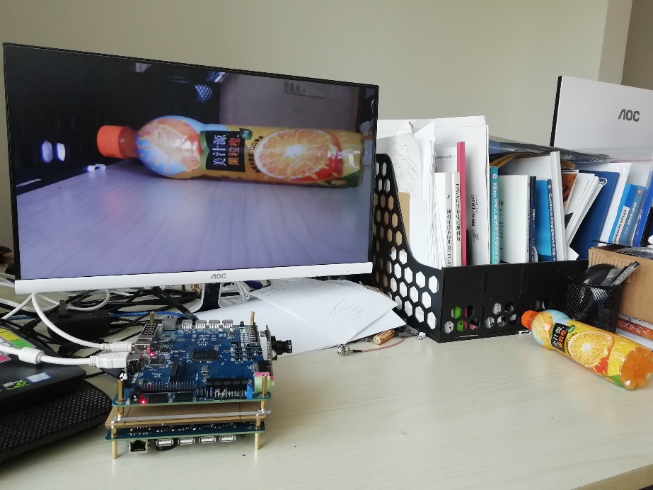
Figure 17.3 Monitor display pictures taken by 5640
Experiment 18 High-speed ADC9226 Acquisition Experiment
18.1 Experiment Objective
Learn about parallel ADC collectors and master the use of ADC9226.
18.2 Experiment Implement
Insert the ADC9226 module face up into the FPGA development board to the GPIO2 and GPIO1 ports which are next to the red-green audio module. Write programs to use this module to test
18.3 Experiment
18.3.1 ADC9226 Module Introduction
ADC9226 module adopts AD9226 chip design of ADI Company. This chip is a monolithic, 12-bit, 65 MSPS analog-to-digital converter (ADC). It uses a single power supply and has an on-chip high-performance sample-and-hold amplifier and voltage reference. It uses a multistage differential pipelined architecture with a data rate of 65 MSPS and guarantees no missing codes over the full operating temperature range.
See Figure 18.1 for ADC9226 timing diagram.
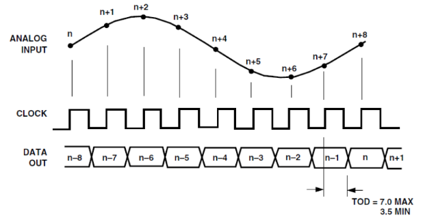
Figure18.1 ADC9226 timing diagram
From this timing diagram, we know that there is no need to configure the AD9226 chip, as long as the appropriate CLOCK is provided, the chip can perform data acquisition.
18.3.2 Program Design
-
-
-
- AD acquisition sub-module
-
-
As can be seen from Figure 18.1, the high bit of AD9226 is bit[0] and the low bit is bit [11], so the data bit order needs to be reversed in the program.
| module ad_9226(
input ad_clk, input [11:0] ad1_in, output reg [11:0] ad_ch ); always @(posedge ad_clk) begin ad_ch[11] <= ad1_in[0] ; ad_ch[10] <= ad1_in[1] ; ad_ch[9 ] <= ad1_in[2] ; ad_ch[8 ] <= ad1_in[3] ; ad_ch[7 ] <= ad1_in[4] ; ad_ch[6 ] <= ad1_in[5] ; ad_ch[5 ] <= ad1_in[6] ; ad_ch[4 ] <= ad1_in[7] ; ad_ch[3 ] <= ad1_in[8] ; ad_ch[2 ] <= ad1_in[9] ; ad_ch[1 ] <= ad1_in[10] ; ad_ch[0 ] <= ad1_in[11] ; end endmodule |
-
-
-
- Data conversion program
-
-
The AD9226 module design uses an internal reference source. VREF is the output port of the reference source, which can be used for 1V and 2V reference voltages. It can be selected through SENCE. When SENCE is grounded, a 2V reference is provided, and when SENCE is connected to VREF, a 1V reference is provided. The module uses a 2V reference power supply. VINA input range is 1.0 ~ 3.0V.
The 22 (12) pin of AD9226 has the function of collecting data selection. There are two input and output data formats of AD9226. For the specific format, refer to the 9226 datasheet. The 22 (12) pin of the AD9226 module in this experiment is connected to high level, so it uses Binary Output Mode. The BCD conversion submodule has been introduced in Experiment 8 and is not repeated here.
-
-
-
- 9226 module AD acquisition range selection
-
-
The attenuation range of the AD acquisition module is divided into gears. Press the UP key on the development board to switch the range.
Table 18.1 Gear shift indication table
Gear comparison table (input voltage percentage) |
Corresponding indicator |
| 4% | led0 lit |
| 8% | led0, led1 lit |
| 20% | led0, led1, led2 lit |
| 40% | led0, led1, led2, led2 lit |
| module range (
input wire clk , input wire rst_n , input wire key , output wire [3:0] led , output wire [1:0] scope ); wire flag_switch ; key_process key_process_inst( .clk (clk) , .rst_n (rst_n) , .key_switch (key) , .flag_switch (flag_switch) ); reg [1:0] scope_st =00 ; reg [3:0] led_temp =4’he ; always @ (posedge clk ,negedge rst_n) begin if (~rst_n) begin scope_st <= 0 ; led_temp <= 4’he ; end else begin case (scope_st) 0: begin led_temp <= 4’he ; if (flag_switch ) scope_st <= 1 ; end 1: begin led_temp <= 4’hc ; if (flag_switch ) scope_st <= 2 ; end 2: begin led_temp <= 4’h8 ; if (flag_switch ) scope_st <= 3 ; end 3: begin led_temp <= 4’h0 ; if (flag_switch ) scope_st <= 0 ; end endcase end end assign led = led_temp ; assign scope = scope_st ; endmodule |
-
-
-
- Main program design
-
-
The main program is divided into three sub-programs, which are AD_9226 acquisition module, data conversion calculation module volt_cal, and voltage value segment display module. The segment display part has been introduced in the previous experiment and will not be introduced here.
| module high_speed_ad_test(
input wire sys_clk, input wire otr , input wire key_switch , input wire sys_rst_n , input wire [11:0] ad1_in, output wire ad1_clk, output wire [5:0] sel, output wire [3:0] led , output wire cain_a, output wire cain_b, output wire [7:0] sm_db ); assign ad1_clk = sys_clk ; assign sm_db={point1, ~sm_db_r }; wire [19:0] ch1_dec; wire [11:0] ad_ch1 ; wire ch1_sig ; wire point1 ; wire [6:0] sm_db_r ; ad_9226 u1 ( .ad_clk (sys_clk), .ad1_in (ad1_in ), .ad_ch (ad_ch1 ) ); volt_cal u2( .ad_clk (sys_clk), .ad_ch1 (ad_ch1), .ch1_dec (ch1_dec), .ch1_sig (ch1_sig) ); led_seg7 u3( .clk (sys_clk), .rst_n (sys_rst_n ), .otr (otr) , .ch1_sig (ch1_sig ), .ch1_dec (ch1_dec), .sel (sel), .point1 (point1), .sm_db (sm_db_r) ); range u4( .clk (sys_clk), .rst_n (sys_rst_n ), .key (key_switch) , .led (led), .scope ({cain_b,cain_a}) ); endmodule |
18.4 Experiment Verification
- Pin assignment
| Signal Name | Port Description | Network Name | FPGA Pin |
| sys_clk | System clock | C10_50MCLK | G21 |
| sys_rst_n | System reset | KEY1 | Y4 |
| lg_en | ADG612 input | IO25 | AB20 |
| hg_en | ADG612 input | IO24 | AA20 |
| ad1_clk | Ad acquisition clock | IO28 | R16 |
| otr | Input voltage overrange flag | IO1 | AA13 |
| sm_db[0] | Segment selection | SEG_PA | B15 |
| sm_db[1] | Segment selection | SEG_PB | E14 |
| sm_db[2] | Segment selection | SEG_PC | D15 |
| sm_db[3] | Segment selection | SEG_PD | C15 |
| sm_db[4] | Segment selection | SEG_PE | F13 |
| sm_db[5] | Segment selection | SEG_PF | E11 |
| sm_db[6] | Segment selection | SEG_PG | B16 |
| sm_db[7] | Segment selection | SEG_DP | A16 |
| sel[0] | Bit selection | SEG_3V3_D0 | E12 |
| sel[1] | Bit selection | SEG_3V3_D1 | F11 |
| sel[2] | Bit selection | SEG_3V3_D2 | E13 |
| sel[3] | Bit selection | SEG_3V3_D3 | E15 |
| sel[4] | Bit selection | SEG_3V3_D4 | D19 |
| sel[5] | Bit selection | SEG_3V3_D5 | F14 |
| ad1_in[0] | AD9226 acquisition data bus | IO0 | V12 |
| ad1_in[1] | AD9226 acquisition data bus | IO5 | Y13 |
| ad1_in[2] | AD9226 acquisition data bus | IO4 | AB13 |
| ad1_in[3] | AD9226 acquisition data bus | IO3 | AB14 |
| ad1_in[4] | AD9226 acquisition data bus | IO6 | W13 |
| ad1_in[5] | AD9226 acquisition data bus | IO2 | R14 |
| ad1_in[6] | AD9226 acquisition data bus | IO7 | AA14 |
| ad1_in[7] | AD9226 acquisition data bus | IO29 | U16 |
| ad1_in[8] | AD9226 acquisition data bus | IO30 | AA15 |
| ad1_in[9] | AD9226 acquisition data bus | IO31 | T16 |
| ad1_in[10] | AD9226 acquisition data bus | IO27 | V16 |
| ad1_in[11] | AD9226 acquisition data bus | IO26 | U17 |
| led0 | Input signal attenuation indicator | LED0 | J5 |
| led1 | Input signal attenuation indicator | LED1 | J6 |
| led2 | Input signal attenuation indicator | LED2 | H5 |
| led3 | Input signal attenuation indicator | LED3 | H6 |
| key_switch | Attenuation switch | PB2 | V5 |
- Board verification
Use this experimental development board to connect the DA9667 module to generate a 1M sine wave as a signal source. Use the AD9226 module to connect to GPIO1 and GPIO2 of the PRA040 development board and apply a logic analyzer to capture the signal as shown in Figure 18.2. The following waveform can be observed. From the left to the right of the segment display, the first segment display is selected and lit to indicate that the input measurement voltage exceeds the AD9226 measurement range (the absolute value of VINA-VINB is less than or equal to the reference voltage, and the reference voltage of this module is 2V). The second segment display shows the sign of the input voltage (VINA-VINB). The last four digits are the input voltage value. When the input signal value is a slowly changing signal, the segment display can display the signal voltage amplitude.
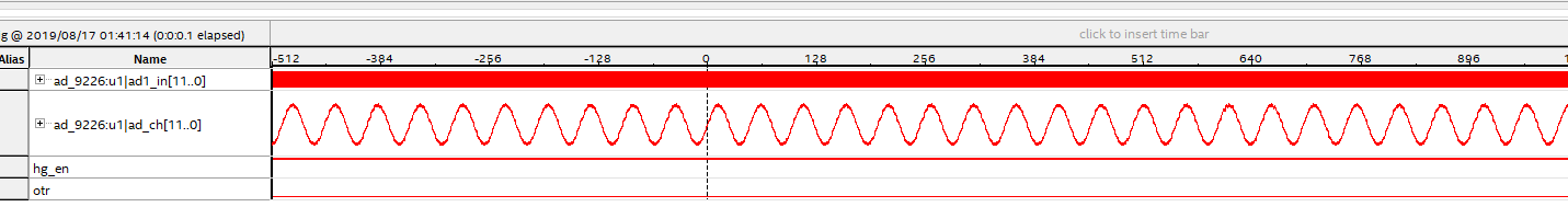
Figure 18.2 Measured signal waveform of AD9226 captured by logic analyzer
Experiment 19 DAC9767 DDS Signal Source Experiment
19.1 Experiment Objective
- Learn about DDS (Direct Digital Synthesizer) related theoretical knowledge.
- Read the AD9767 datasheet and use the AD9767 to design a signal source that can generate sine, square, triangle, and sawtooth waves.
19.2 Experiment Implement
- Learn about DDS theoretical knowledge.
- On the basis of understanding the principle of DDS, combined with the theoretical knowledge, use AD9767 module and development board to build a signal source whose waveform, amplitude and frequency can be adjusted. (There are no specific requirements for the adjustment of waveform, amplitude, and frequency here, as long as the conversion can be adjusted by pressing a button).
19.3 Experiment
19.3.1 DDS Introduction
The DDS technology is based on the Nyquist sampling theorem. Starting from the phase of the continuous signal, the sine signal is sampled, encoded, and quantized to form a sine function table, which is stored in the ROM. During synthesis, phase increment is changed by changing the frequency word of the phase accumulator. Phase increment is what is called step size. The difference in phase increment results in different sampling points in a cycle. When the clock frequency, or the sampling frequency does not change, the frequency is changed by changing the phase. The block diagram is shown in Figure 19.1.
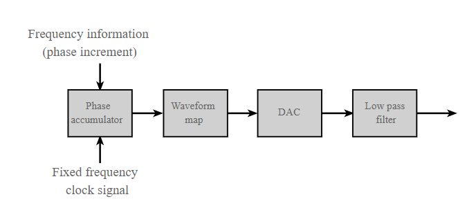
Figure 19.1 DDS block diagram
19.3.2 AD9767 Configuration Introduction
The AD9767 module uses ADI’s AD9767 DAC chip, which is a 14-bit, 125MSPS conversion rate high-performance DAC device. It supports the IQ output mode and can be used in the communications.
AD9767 interface timing requirements. As shown in Figure 19.2 below, when the rising edge of the clock comes, the data must remain stable for ts time. After the rising edge of the clock, the data must remain stable for th to be correct.
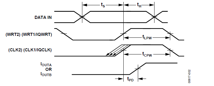
Figure 19.2 9767 interface timing diagram
19.3.3 Waveform Memory File Configuration
The waveform storage area file is dds_4096x10b_wave_init.coe. For the specific making process, refer to the use of the *.coe file in the experiment 9. The file containing the waveform information is stored in the ROM. After the project file is programmed into the FPGA, the FPGA directly reads the waveform information from the ROM and sends it to the AD9767 interface, and then outputs the corresponding waveform on the AD9767 module. The waveform storage is as shown in Figure 19.3.
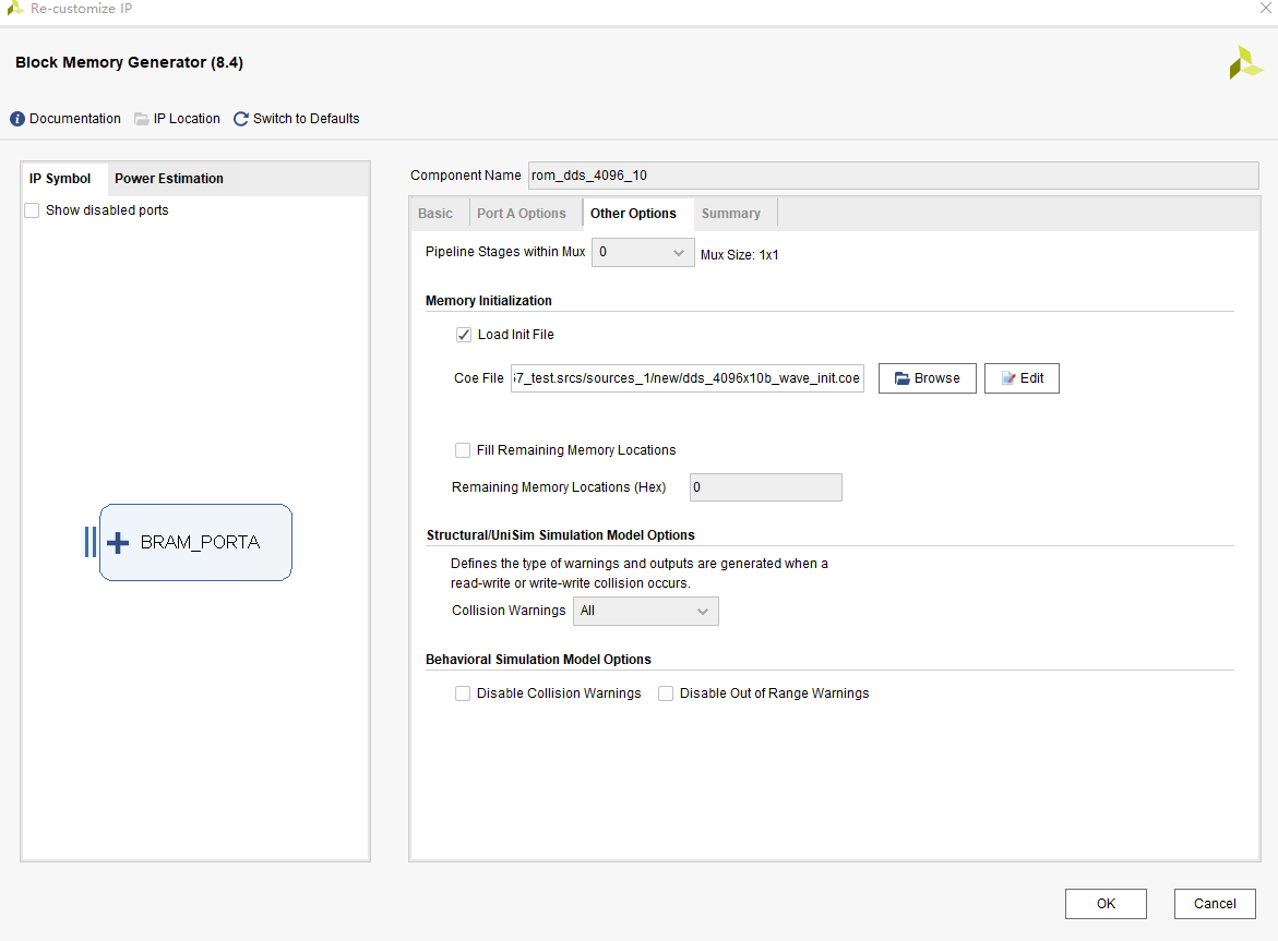
Figure 19.3 Wave file storage
19.3.4 Program Design
1.The main program includes waveform selection, mode selection, frequency adjustment, and amplitude adjustment. The specific code is as follows:
| module dac_9767_test(
input wire sys_clk_50m, input wire rst_n, (*mark_debug=”true”*) output mode, output wire dac_clk, output wire led , input wire mode_adjust, input wire a_adjust, input wire f_adjust, input wire wave_adjust, output reg [13:0] data_out ); wire [9:0] douta ; wire clk_50m ; BUFG BUFG_inst ( .O(clk_50m), .I(sys_clk_50m) ); wire locked ; wire clk_100m ; pll_50_100 pll_50_100_inst ( .clk_out1(clk_100m), .clk_out2(dac_clk), //nclk_100m .reset(0), .locked(locked), .clk_in1(clk_50m)); reg rst_n_g = 0 ; always @ (posedge clk_100m) rst_n_g<=locked &rst_n ; wire A_ctrl ; wire F_ctrl ; wire wave_switch ; wire mode_ctrl ; reg [1:0] base_addr =0 ; reg [3:0] base_A =0 ; reg [1:0] a_st =0 ; always @ (posedge clk_100m , negedge rst_n_g ) begin if (~rst_n_g) base_addr <=0; else if (wave_switch) base_addr <= base_addr +1 ; else base_addr <= base_addr ; end always @ (posedge clk_100m , negedge rst_n_g ) begin if (~rst_n_g) begin base_A <=1; a_st <=0; end else begin case (a_st) 0: begin base_A <=8; a_st <=1; end 1: begin if (A_ctrl) begin a_st<=2 ; base_A <=11; end else begin a_st<=1 ; base_A <=8; end end 2: begin if (A_ctrl) begin a_st<=3; base_A <=15; end else begin a_st<=2; base_A <=11; end end 3: begin if (A_ctrl) begin a_st<= 1; base_A <=8; end else begin a_st<=3 ; base_A <=15; end end default :begin base_A <=1; a_st <=0; end endcase end end always @ (posedge clk_100m , negedge rst_n_g ) begin if (~rst_n_g) data_out <=0 ; else data_out<= douta * base_A ; end reg [9:0] addr_r =0; reg [9:0] addr_temp_F =1 ; reg [3:0] f_st =0 ; always @ (posedge clk_100m , negedge rst_n_g ) begin if (~rst_n_g) begin addr_temp_F <= 0; f_st <=0 ; end else begin case (f_st) 0 : begin addr_temp_F <= 0 ; f_st <= 1 ; end 1 : begin addr_temp_F <= 1 ; if (F_ctrl) f_st <= 2 ; end 2 : begin addr_temp_F <= 2 ; if (F_ctrl) f_st <= 3 ; end 3 : begin addr_temp_F <= 3 ; if (F_ctrl) f_st <= 4 ; end 4 : begin addr_temp_F <= 4 ; if (F_ctrl) f_st <= 5 ; end 5 : begin addr_temp_F <= 5 ; if (F_ctrl) f_st <= 6 ; end 6 : begin addr_temp_F <= 6 ; if (F_ctrl) f_st <= 7 ; end 7 : begin addr_temp_F <= 8 ; if (F_ctrl) f_st <= 1 ; end default : f_st <= 1 ; endcase end end always @ (posedge clk_100m , negedge rst_n_g ) begin if (~rst_n_g) addr_r <=0; else addr_r <=addr_r+1+addr_temp_F ; end (*mark_debug=”true”*)reg [11:0] addra=0 ; always @ (posedge clk_100m , negedge rst_n_g ) begin if (~rst_n_g) addra <=0 ; else addra<={base_addr, addr_r }; end reg mode_r=0; always @ (posedge clk_100m , negedge rst_n_g ) begin if (~rst_n_g) mode_r <=0 ; else if (mode_ctrl) mode_r <=~mode_r; else mode_r <= mode_r ; end assign mode=mode_r ; assign led= ~mode_r ; key_process ( .clk (clk_100m ) , .rst_n (rst_n_g ) , .key_switch (wave_adjust) , .key_adjust (a_adjust ) , .key_add (f_adjust ) , .key_sub (mode_adjust) , .flag_switch (wave_switch) , .flag_adjust (A_ctrl ) , .flag_add (F_ctrl ) , .flag_sub (mode_ctrl ) ); rom_dds_4096_10 rom_dds_4096_10_inst ( .clka(clk_100m), // input wire clka .addra(addra), // input wire [11 : 0] addra .douta(douta) // output wire [9 : 0] douta ); endmodule |
19.4 Experiment Verification
1. Pin assignment
| Signal Name | Port Description | Network Name | FPGA Pin |
| sys_clk_50m | System clock | C10_50MCLK | G21 |
| mode | 9767 mode control | IO24 | AA14 |
| wave_adjust | Waveform selection | key2 | V5 |
| a_adjust | Amplitude selection | key3 | Y6 |
| f_adjust | Frequency selection | key4 | AB4 |
| mode_adjust | Mode selection | key6 | AA4 |
| led | Mode indicator light | LED0 | J5 |
| dac_clk | 9767 driving clock | IO28 | W13 |
| rst_n | System reset | key1 | Y4 |
| data_out[0] | AD9767 data bus | IO1 | U16 |
| data_out[1] | AD9767 data bus | IO0 | AA15 |
| data_out[2] | AD9767 data bus | IO5 | T16 |
| data_out[3] | AD9767 data bus | IO4 | V16 |
| data_out[4] | AD9767 data bus | IO3 | U17 |
| data_out[5] | AD9767 data bus | IO6 | R16 |
| data_out[6] | AD9767 data bus | IO2 | AB20 |
| data_Out[7] | AD9767 data bus | IO7 | AA20 |
| data_out[8] | AD9767 data bus | IO29 | AA13 |
| data_out[9] | AD9767 data bus | IO30 | Y12 |
| data_out[10] | AD9767 data bus | IO31 | Y13 |
| data_out[11] | AD9767 data bus | IO27 | AB13 |
| data_out[12] | AD9767 data bus | IO26 | AB14 |
| data_out[13] | AD9767 data bus | IO25 | R14 |
2.Board verification
After the FPGA development board is programmed, press the right key (mode), and the mode indicator led0 lights up.
Then waveform can be chosen according to UP key (waveform selection), RETURN key (amplitude selection), LEFT key (frequency selection). (This experiment is only to introduce the theoretical knowledge of DDS and verify its correctness. Therefore, only four types of waveforms are set, which are sine wave, square wave, triangle wave, and sawtooth wave. The frequency and amplitude are also randomly set.) Figure 19.4 below shows four waveforms of the oscilloscope measuring the output of the 9767 module.
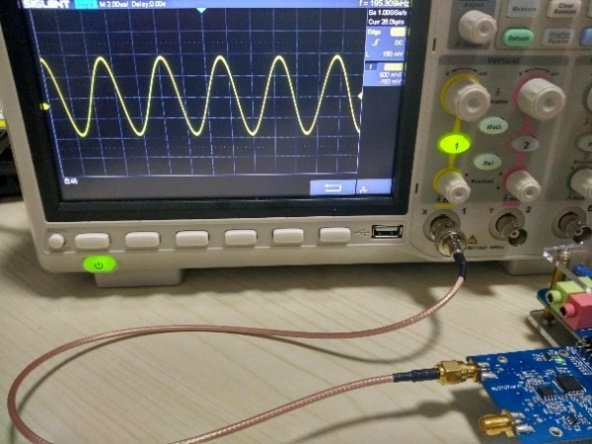
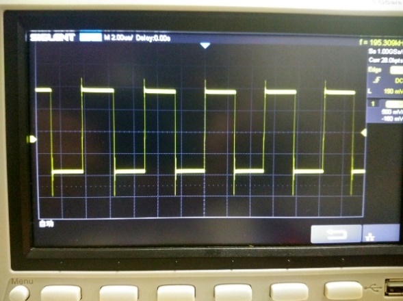
Figure 19-4a Sine wave Figure 19-4b Square wave
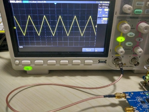
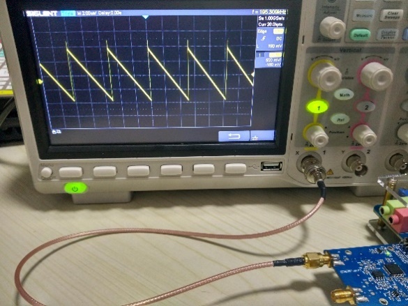
Figure 19-4c Triangle wave Figure 19-4d Sawtooth wave
References:
- https://www.intel.com/content/dam/www/programmable/us/en/pdfs/literature/ug/ug_usb_blstr_ii_cable.pdf
- https://www.nxp.com/docs/en/data-sheet/PCF8591.pdf
- https://www.analog.com/media/en/technical-documentation/user-guides/ADV7511_Hardware_Users_Guide.pdf
- https://www.mouser.com/ds/2/268/atmel_doc0180-1065439.pdf
- https://www.verical.com/datasheet/realtek-semiconductor-phy-rtl8211e-vb-cg-2635459.pdf’
- https://www.mouser.com/ds/2/76/WM8978_v4.5-1141768.pdf
- https://www.mouser.com/datasheet/2/76/WM8978_v4.5-1141768.pdf