FII-PRX100T User Experiment Manuals (newly updated 2020-09-28)

PRX100 USER experimental manual
PRX100 EXPERIMENTAL INSTRUCTIONS

FRASER INNOVATION INC
December 11, 2019
Version Control
|
Contents:
Part 1 FII-PRX100 Development System Introduction 6
3. Human-computer Interaction Interface 6
4. Software Development System 7
Part 2 FII-PRX100 Main Hardware Resources Usage and FPGA Development Experiment 7
2. Create A New Project Under Vivado 7
Experiment 2 Switches and display 26
Experiment 3 Basic Digital Clock Experiment and Programming of FPGA Configuration Files 32
4.Configure the Serial Flash Programming 38
Experiment 4 Block/SCH Digital Clock Design 44
Experiment 5 Button Debounce Design and Experimental Experiment 53
Experiment 6 Digital Clock Comprehensive Design Experiment 60
3.Create an XDC File to Constrain the Clock 71
Experiment 7 Multiplier Use and ISIM Simulation 73
3.The Top-level Entity Is as Follows: 75
4.ISIM Simulation Library Compilation and Call 75
Experiment 8 Hexadecimal Number to BCD Code Conversion and Application 80
2.Application of Hexadecimal Number to BCD Number Conversion 84
Experiment 10 Use Dual_port RAM to Read and Write Frame Data 100
4.Lock the Pins, Compile, and Download to The Board to Test 108
5.Use ILA to Observe Dual_port RAM Read and Write 110
6.Experiment Summary and Reflection 111
Experiment 11 Asynchronous Serial Port Design and Experiment 112
Experiment 12 IIC Protocol Transmission 144
3.Introduction to the IIC Agreement 144
5.Downloading to The Board 154
Experiment 13 AD, DA Experiment 156
4.Downloading to The Board 169
Experiment 14 HDMI Graphic Display Experiment 171
15.4 Experiment Verification 203
Experiment 16 8978 Audio Loopback Experiment 207
16.4 Experiment Verification 223
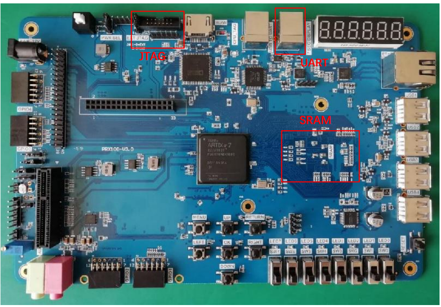
Experiment 17 Reading Experiment of Serial Port Partition of Static Memory SRAM 225
Experiment 18 Photo Display Experiment of OV5640 Camera 236
18.4 Experiment Board Verification 254
Experiment 19 High-speed ADC9226 Acquisition Experiment 259
19.4 Experiment Verification 264
Experiment 20 DAC9767 DDS Signal Source Experiment 266
20.4 Experiment Varification 273
Part 1 FII-PRX100 Development System Introduction
The main purpose of this system design is to complete FPGA learning, development and experiment with Xilin-Vivado. The main device uses the Xilinx-XC7A100T-2FGG676I and is currently the latest generation of FPGA devices from Xilinx. The main learning and development projects can be completed as follows:
- Basic FPGA design training
- Construction and training of the SOPC (Microblaze) system
- IC design and verification, the system provides hardware design, simulation and verification of RISC-V CPU
- Development and application based on RISC-V
- The system is specifically optimized for hardware design for RISC-V system applications
- System Resource
- Extended memory
- Use two Super SRAMs in parallel to form a 32-bit data interface with a maximum access space of 1M bytes.
- IS61WV25616 (2 pieces) 256K x 16bit
- Serial flash
- Spi interface serial flash (128M bytes)
- Serial EEPROM
- Gigabit Ethernet: 100/1000 Mbps
- USB to serial interface: USB-UART bridge
- Human-computer Interaction Interface
- 8 toggle switches
- 8 push buttons
- Definition of 7 push buttons: up, down, left, right, ok, menu, return
- 1 for reset: Reset button
- 8 LEDs
- 6 7-segment decoders
- I2C bus interface
- UART external interface
- Two JTAG programming interfaces: One is for downloading the FPGA debug interface, and the other one is the JTAG debug interface for the RISC-V CPU
- Built-in RISC-V CPU software debugger, no external RISC-V JTAG emulator required
- 4 12-pin GPIO connectors, in line with PMOD interface standards
- Software Development System
- Vivado 18.1 and later version for FPGA development, Microblaze SOPC
- Freedom Studio-Win_x86_64 Software development for RISC-V CPU
- Supporting Resources
RISC-V JTAG Debugger
Xilinx JTAG Download Debugger
FII-PRX100 Development Guide
Part 2 FII-PRX100 Main Hardware Resources Usage and FPGA Development Experiment
This part mainly guides the user to learn the development of FPGA program and the use of onboard hardware through the development example of FPGA. At the same time, the application system software Xilinx is introduced from the elementary to the profound. The development exercises covered in this section are as follows:
Experiment 1 LED Shifting
- Practice how to use the development system software Vivado to establish a new project, call the system resource PLL to establish the clock.
- Write Verilog HDL program to achieve frequency division
- Write Verilog HDL program to implement LED shifting
- Combine hardware resources for FPGA pin configuration
- Compile
- Download the program to the develop board
- Observe the experimental result and debug the project
2. Create A New Project Under Vivado
- Start Vivado in the start Menu. See Figure 1.1
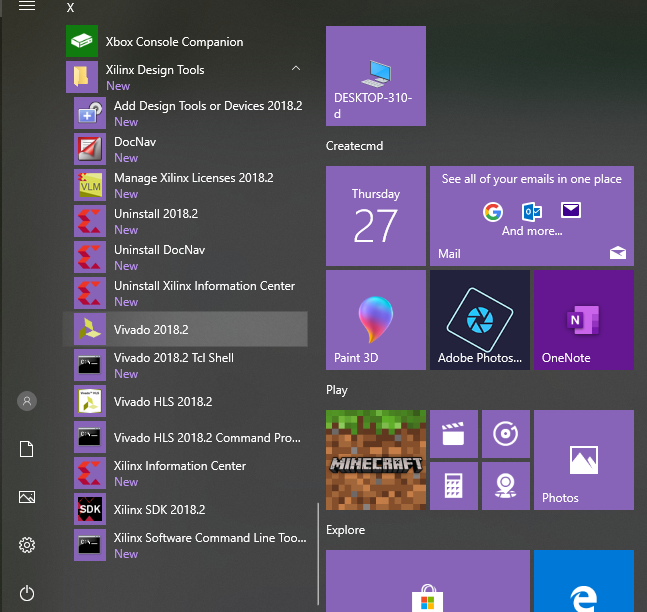
Figure 1.1 Start Menu
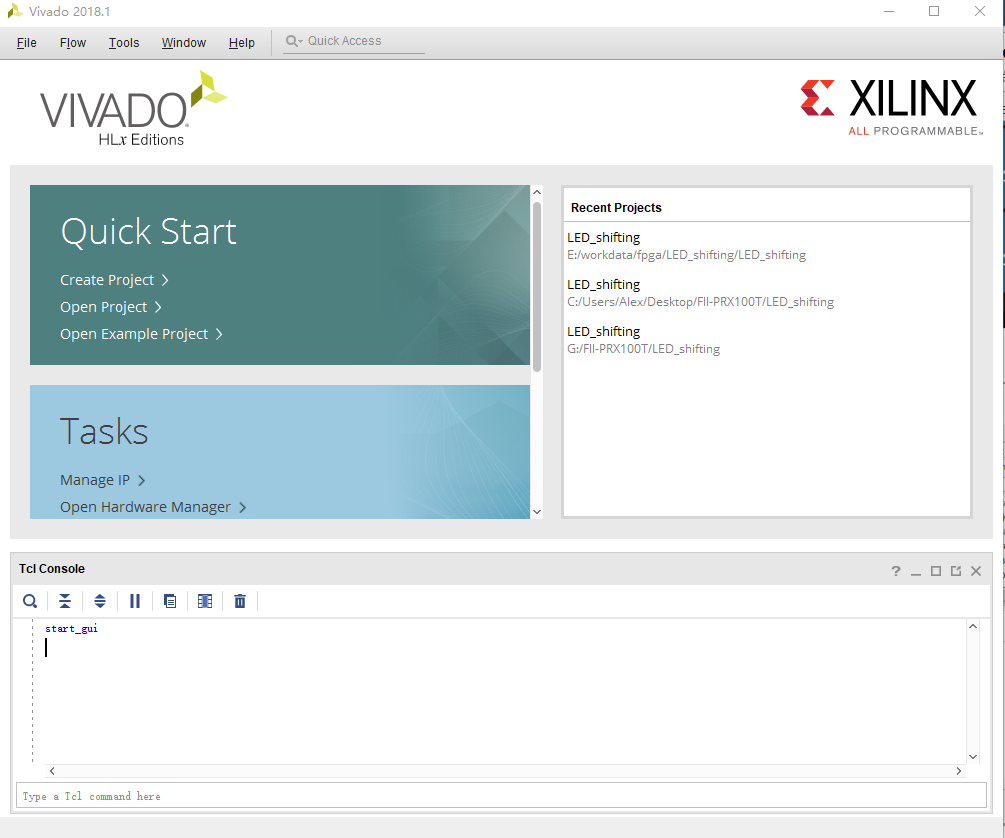
Figure 1.2 Initial interface of Vivado
- File -> Project -> NEW
- Click the Next option button in the pop-up dialog box. Then pop up the setup project interface of Figure 1.3 and Figure 1.4
Figure 1.3 Create a new project
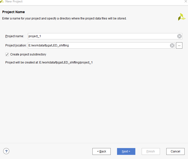
Figure 1.4 Set the project path
Set the project name, project path. Note that the top-level file name must be consistent with the file name of the subsequent top-level file of Verilog. The top-level file name is case-sensitive.
-
- Choose RTL Project to be the project type. See Figure 1.5.
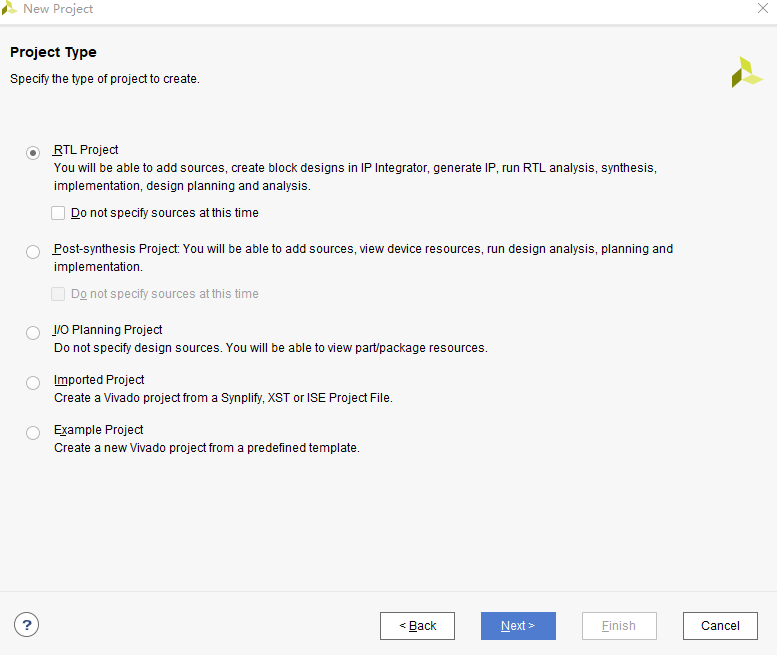
Figure 1.5 Project type selecting
-
- Click Next as shown in Figure 1.6 (there is no source file that can be added since it is new)
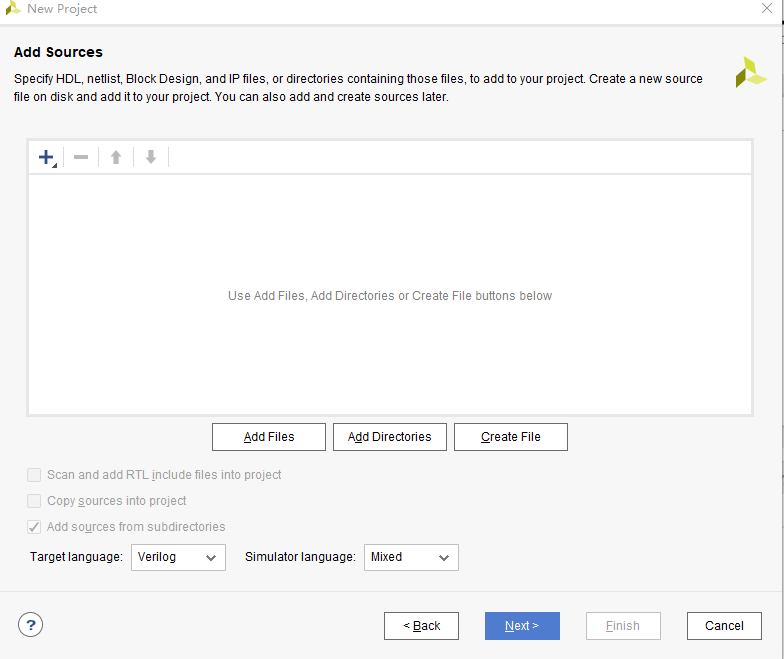
Figure 1.6 Add source file
-
- Click Next as shown in Figure 1.7 (there are no files that can be added to constrain due to it is a new project)
Figure 1.7 Add constrains
-
- Select XC7A100TFGG676-2 in the selection dialog box. See Figure 1.8, click NEXT, then Finish to complete the project building.
Figure 1.8 Choose the default Xilinx part or board
- Create a Verilog HDL file, LED_shifting.v
- Select File -> Add Sources or add the RTL file as shown in Figure 1.9 or Figure 1.10 below.
Figure 1.9 Add source file
Figure 1.10 Add source file
-
- See Figure 1.11, select Add or create design sources and then click Next.
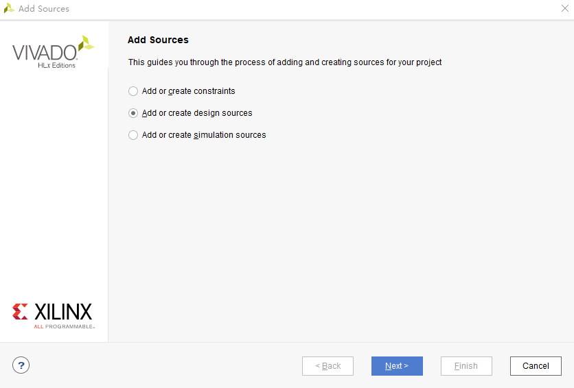
Figure 1.11 Add source file 1
-
- Click Create File. In the popup window, select the Verilog HDL for the file type. Fill in the file name and location -> OK -> Finish. See Figure 1.12.
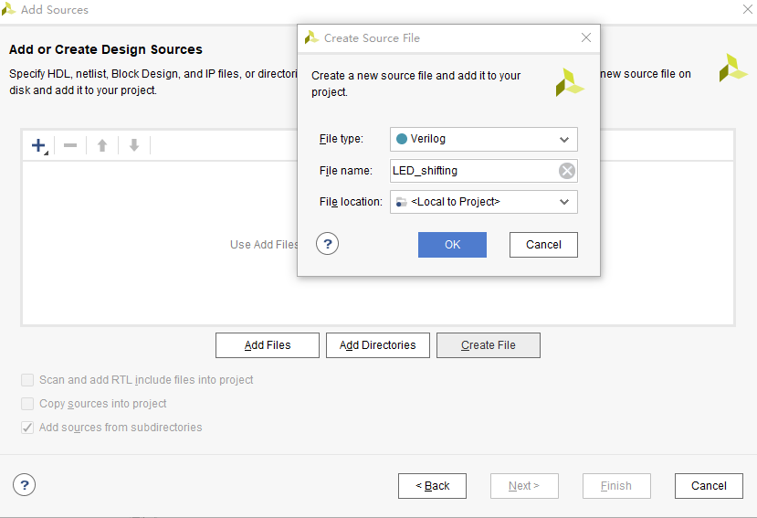
Figure 1.12 Add source file 2
-
- As shown in Figure 1.13, if filling the module name wrongly in the previous step, the name can be modified here. Input and output pin configuration can also be directly set here through the I/O port definitions. (You can also write the generated pin information in the Verilog code later.) Then click OK.
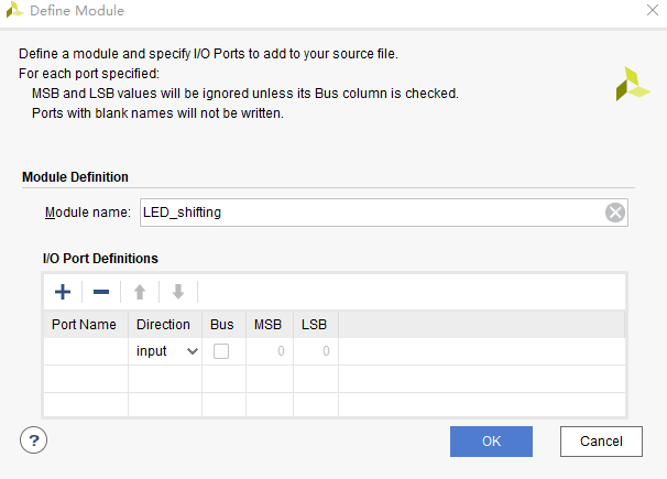
Figure 1.13 Confirmation
-
- Vivado’s sources window generates an LED_shifting RTL file. Click on the file to edit the code. See Figure 1.14.
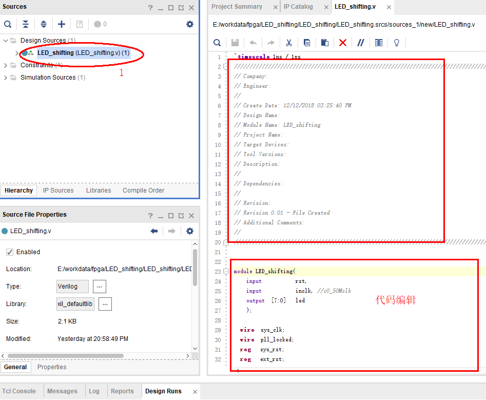
Code here
Figure 1.14 Source file editing
-
- Edit interface file
module Led_shifting(
input rst,
input inclk, //c0_50Mclk
output [7:0] led
);
endmodule
- Add clock module
See Figure 1.15, click the IP Catalog option on the left side of the main interface to pop up the corresponding core supported by the engineering chip. Find the needed IP core by functions or names, or by fast searching. Entering clocking in step 1, then click Clocking Wizard shown in step 2. The clock IP configuration interface will appear after that.
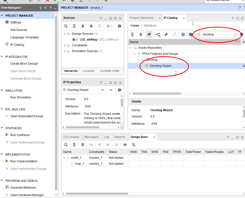
Figure 1.15 PLL IP core setting
-
-
- Enter the clock setting as shown below
- Select either MMCM or PLL here. Here is an example of selecting a PLL core.
- The path filled in Figure 1.16 is the setting of the clock file path. Figure 1.17 shows the name setting.
- See Figure 1.18, clk_in1 (which is the input clock of the PLL, where there is only one input clock) is set to be 50 MHz, which is consistent with the clock provided by the hardware board.
- Other PLL settings can be selected by default. If the required functions involve advanced features, use the official reference for more.
- Click the Output Clocks tab to set the PLL compensation output clock to clk_out1.
- For PLL asynchronous reset control and capture lock status settings, use the default mode shown in the figure.
- Enter the clock setting as shown below
-
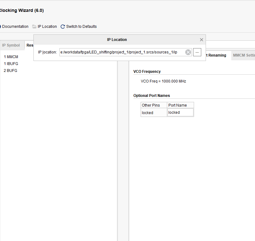
Figure 1.16 IP location setting window
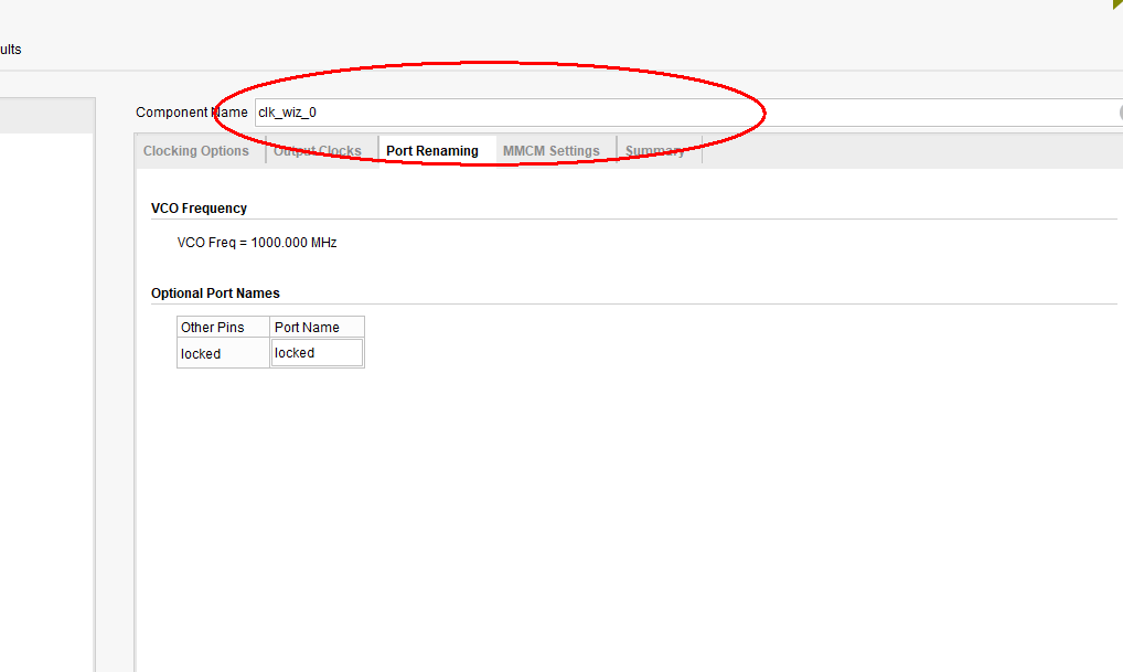
Figure 1.17 IP core name setting
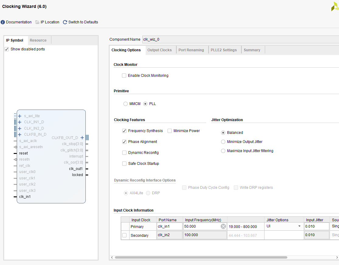
Figure 1.18 PLL input clock setting
-
-
-
- See Figure 1.19, set the output frequency to 100 MHz, the phase offset to 0, and the duty cycle to 50%. Click OK.
-
-
Figure 1.19 Output frequency and duty cycle setting
-
-
-
- Click Generate to finish the IP core setting. See Figure 1.20.
-
-
Figure 1.20 Generate IP core
-
-
-
- After the clock module is generated, select the IP Sources sub-tab in the Labels box of the Sources of the project interface, that is, the IP core file can be found just after the generation. See Figure 1.21.
- Instantiate the module to the top-level entity
-
-
Figure 1.21 Instantiate to the top-level entity
The code is as follows:
-
-
-
- Top-level entity instance
- Key signal description
-
-
sys_rst, the value before the PLL lock is ‘1’ as a reset signal for the entire system. After the system is locked (pll_locked == 1’b1), the value of sys_rst becomes ‘0’. At the same time, it is driven by the rising edge of sys_clk, so it is a synchronous reset signal.
|
Note that the user is already familiar with the Verilog syntax by default, so the Verilog syntax is not exhaustive here.
- Frequency division design
-
- The system clock is 100 MHz, while the speed of the LED blinking is set to be 1 second, so frequency division is needed.
- Microsecond frequency division
-
The Verilog HDL code is as follows:
|
-
-
- Millisecond frequency division
-
|
-
-
- Second frequency division
-
|
-
-
- LED shifting design
-
|
Because the schematics design uses FPGA I/O sink current mode, it must be inverted bitwise before output. Otherwise, it will show that each time 7 LEDs are lit, only one LED is left in the non-lighting state.
Assign led=~led_r; //Bitwise inverse
The pin assignment table of the program is as follows:
| Signal Name | Port Description | Network Label | FPGA Pin |
| inclk | System clock 50 MHz | C10_50MCLK | U22 |
| rst | Reset, high by default | KEY1 | M4 |
| led0 | LED 0 | LED0 | N17 |
| led1 | LED 1 | LED1 | M19 |
| led2 | LED 2 | LED2 | P16 |
| led3 | LED 3 | LED3 | N16 |
| led4 | LED 4 | LED4 | N19 |
| led5 | LED 5 | LED5 | P19 |
| led6 | LED 6 | LED6 | N24 |
| led7 | LED 7 | LED7 | N23 |
Figure 1.22 Schematics for LED
Figure 1.23 FPGA input clock
- After the code is integrated, there are two ways to add the constraint file. One is to use the I/O planning function in Vivado, and the other is to directly create a constraint file for the XDC and manually enter the constraint command. Here the first method is adopted for now, I/O planning function. The procedure is as follows
-
- Go to Flow Navigator -> Synthesis -> Run Synthesis, integrate the project first. See Figure 1.24. The purpose is:
- Check the syntax error
- Form the tree hierarchy of the project
- Go to Flow Navigator -> Synthesis -> Run Synthesis, integrate the project first. See Figure 1.24. The purpose is:
-
Figure 1.24 Check the syntax, compilation synthesis
After the integration is complete, select Open Synthesized Design, open the comprehensive results, select I/O Planning under layout, and assign the pins in the I/O port section in the figure below.
Figure 1.25 Pin assignment
-
- After the pin assignment is completed, click Run Implementation as shown in Figure 1.26. After the completion of the Generate Bitstream, generate a downloadable bit file. Click Open Hardware Manager to link to the device. See Figure 1.27.
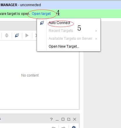
Figure 1.26 Generate bit files Figure 1.27 Connect with the experiment board
-
- As shown in Figure 1.28 below, select the correct bit file and download the bit file settings.
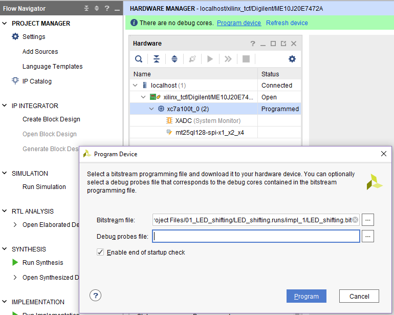
Figure 1.28 Download the bit file configuration
-
- Click Program to download the program to the board to test
-
- The hardware connection is shown as follows, the 8 LEDs blink one by one.
-
- Click Program to download the program to the board to test
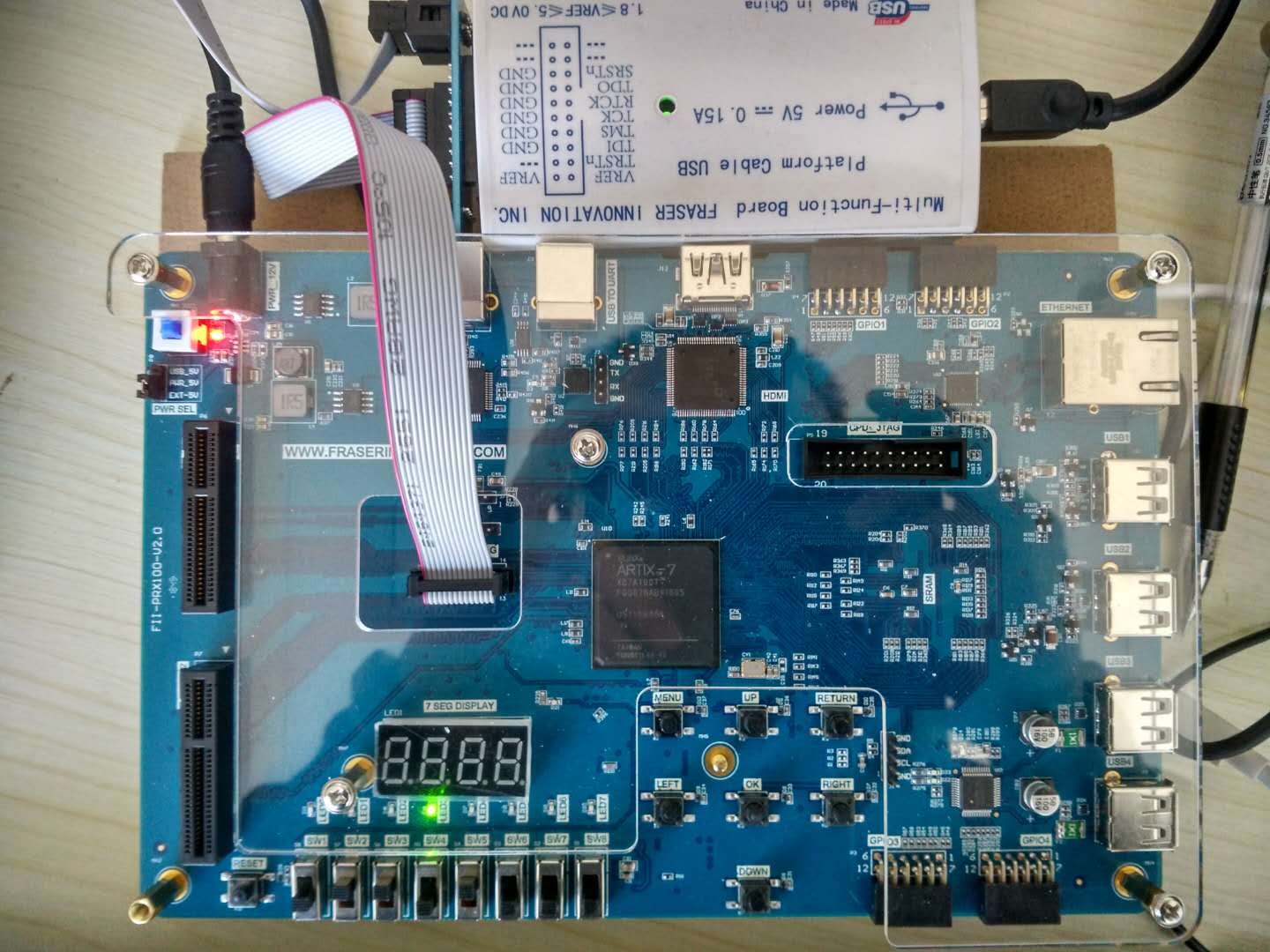
Figure 1.29 Develop board
-
-
-
- Review the above steps to be proficient in each process
-
-
Experiment 2 Switches and display
1.Experiment Objective
-
- Continue to practice using develop board
- Learn to use ILA (Integrated Logic Analyzer) in Vivado
- Learn to use the FPGA configuration memory for programming
2.Start New Project
-
- Refer to Experiment 1
- Select the same chip in Experiment 1
- Add PLL1 (Here PLL1 is optional, external input clock can be used directly)
3.Verilog HDL Code
|
Schematics of develop board
-
- See Figure 2.1. the diodes D19-D26 are mainly used to eliminate the damage of the FPGA pin caused by human body contact static electricity.
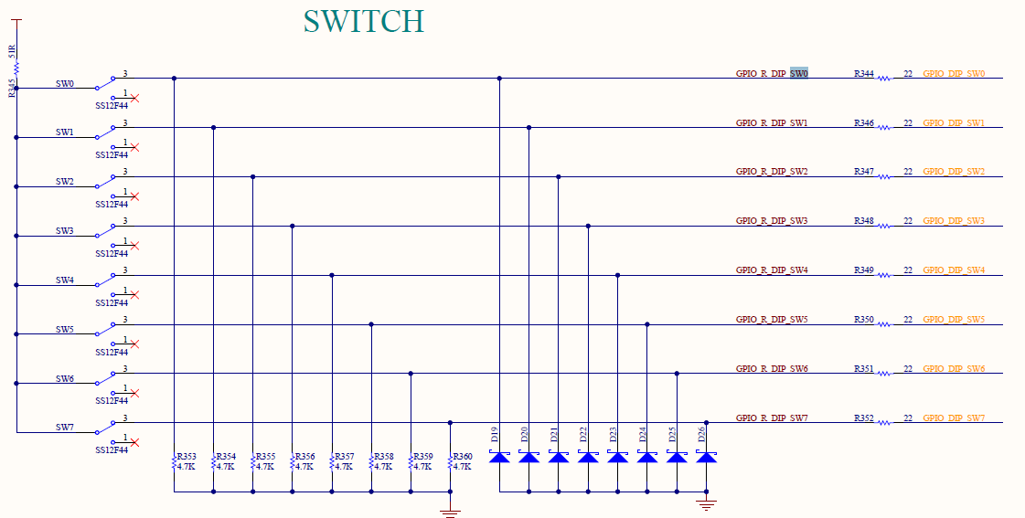
Figure 2.1 Switches drive the circuit
4.FPGA Pin Assignment
| Signal Name | Port Description | Network Label | FPGA Pin |
| inclk | System Clock 50 MHz | C10_50MCLK | U22 |
| rst | Reset, high by default | KEY1 | M4 |
| led0 | LED 0 | LED0 | N17 |
| led1 | LED 1 | LED1 | M19 |
| led2 | LED 2 | LED2 | P16 |
| led3 | LED 3 | LED3 | N16 |
| led4 | LED 4 | LED4 | N19 |
| led5 | LED 5 | LED5 | P19 |
| led6 | LED 6 | LED6 | N24 |
| led7 | LED 7 | LED7 | N23 |
| SW0 | SW 0 | GPIO_DIP_SW0 | N8 |
| SW1 | SW 1 | GPIO_DIP_SW1 | M5 |
| SW2 | SW 2 | GPIO_DIP_SW2 | P4 |
| SW3 | SW 3 | GPIO_DIP_SW3 | N4 |
| SW4 | SW 4 | GPIO_DIP_SW4 | U6 |
| SW5 | SW 5 | GPIO_DIP_SW5 | U5 |
| SW6 | SW 6 | GPIO_DIP_SW6 | R8 |
| SW7 | SW 7 | GPIO_DIP_SW7 | P8 |
5.Program in Vivado
6.Download to the develop board to test and dial the DIP switch to see the corresponding LED light on and off. See Figure 2.2.
Figure 2.2 Experiment result
7.Use of ILA
- Choose top-level entity SW_LED.v file to Run Synthesis
- After the integration is complete, under the Netlist window, all network nodes present in the current design are listed. Debug the network nodes. See Figure 2.3.
Figure 2.3 Mark debugged network nodes
-
- In the Vivado main interface menu, execute the menu command Tool -> Set up Debug. In the popup window, there is clock domain of the selected debug signal. The clock domain of sw_IBUF is red. See Figure 2.4.
Figure 2.4 Debugged network node clock domain setting
-
- In the red circle shown in Figure 2.4, right click to set the clock domain.
Figure 2.5 Modify the debugged network node clock domain
-
- After the setting is completed, click Next. The popup window is shown in Figure 2.6. Set the data collection depth and select the check box in front of Capture control and Advance trigger. Then keep clicking Next until the end.
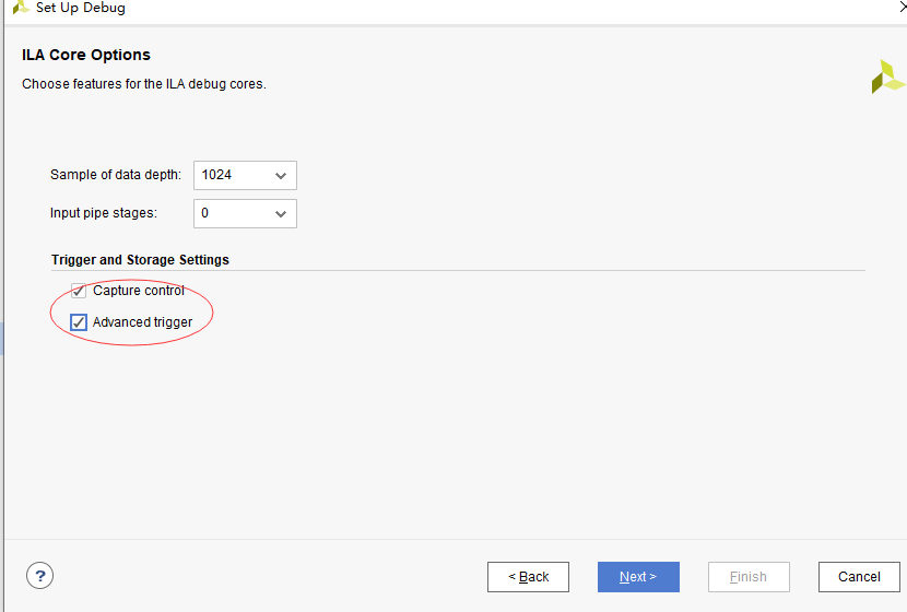
Figure 2.6 Set the data collection depth
-
- Add I/O pin constraint information for implementation. Then generate a bit file and download it to FPGA. The debugging interface is automatically popped up. Click the icon button to see the following results. The test results in the debug diagram below Figure 2.7 indicate that the design results are correct.
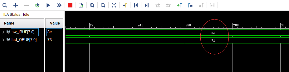
Figure 2.7 Debug
When the input of switch is high, the input LED pin is controlled to be low, and the LED is lit. The figure for the experiment result on board from above shows that the input sw is 10001100 and the LED light is 01110011. The hexadecimal is 8c and 73 respectively. It is consistent with the ILA test results in the figure above.
- Modify the trigger condition to test the output under different trigger conditions
Experiment 3 Basic Digital Clock Experiment and Programming of FPGA Configuration Files
1.Experiment Objective
-
- Review the contents of experiment 1 and experiment 2, master the configuration of PLL, the design of frequency divider, the principle of schematics and the pin assignment of FPGA.
- Study BCD decoder
- Display design of 4-digit hexadecimal to 7 segment display decoders
- Generate a programmable configuration file and program it to the serial FLASH of the development board through the JTAG interface.
2.Design of The Experiment
-
- Refer experiment 1 for building new projects, chip selection
|
-
- Add PLL, the input clock is 50 MHz, and the output clock is 100 MHz. Refer experiment 1 for more information
|
-
- Add microsecond, millisecond, and second frequency dividers. Refer to experiment 1.
|
-
- Minute and second frequency divider
|
-
- Learn the schematics of the common anode segement decoder and the connection between the scanning circuit and the FPGA.
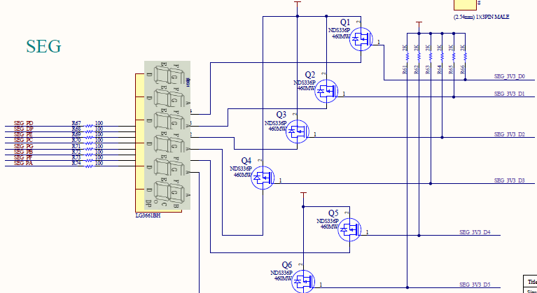
Figure 3.1 Common anode segment decoder schematics
-
-
- The pins of segment display decoder are shown in Figure 3.1. This is a schematic diagram of the six decoders combined. The pin names A, B, C, D, E, F, and G (corresponding connections are SEG_PA, SEG_PB, SEG_PC, SEG_PD, SEG_PE, SEG_PF, SEG_PG) correspond to the 7 segments of the decoder, and the DP (corresponding connection is SEG_PD)corresponds to the 8th segment, which is commonly used as a decimal point display.
-
A, B, C, D, E, F, G, D, P select which segment of the decoder will lit. The segment to be lit corresponds to the low point.
Illumination of segment decoders is controlled by the bit selection lines SEG_3V3_D0, SEG_3V3_D1, SEG_3V3_D2, SEG_3V3_D3, SEG_3V3_D4, SEG_3V3_D5.
-
-
- Code for the segment display decoder
-
|
-
-
- Dynamic canning
-
The dynamic scanning of the segment display decoder utilizes the visual persistence characteristic of the human eye, and in addition to the speed of change that the human eye can distinguish, the segment corresponding to each decoder is quickly and time-divisionally illuminated. Because the time taken to illuminate all the decoders is less than the visual persistence of the human eye, in the eyes of the people, these decoders are continuously lit at the same time, and there is no feeling of flickering.
|
3.FPGA Pin Assignment
| Signal Name | Port Description | Network Label | FPGA Pin |
| inclk | System clock 50 MHz | C10_50MCLK | U22 |
| rst | Reset, high by default | KEY1 | M4 |
| seven_seg[0] | Segment a | SEG_PA | K26 |
| seven_seg[1] | Segment b | SEG_PB | M20 |
| seven_seg[2] | Segment c | SEG_PC | L20 |
| seven_seg[3] | Segment d | SEG_PD | N21 |
| seven_seg[4] | Segment e | SEG_PE | N22 |
| seven_seg[5] | Segment f | SEG_PF | P21 |
| seven_seg[6] | Segment g | SEG_PG | P23 |
| seven_seg[7] | Segment h | SEG_DP | P24 |
| scan[0] | Segment 1 | SEG_3V3_D0 | R16 |
| scan[1] | Segment 2 | SEG_3V3_D1 | R17 |
| scan[2] | Segment 3 | SEG_3V3_D2 | N18 |
| scan[3] | Segment 4 | SEG_3V3_D3 | K25 |
-
- Lock the pin, compile, and download the program to the develop board
- Observe the test result

Figure 3.2 Segment decoder illuminates
4.Configure the Serial Flash Programming
-
- The schematics of configuring serial Flash is as follows:
Figure 3.3 Schematics of Serial Flash interface
-
- Configure FLASH and FPGA pin mapping
| FLASH | *SPI_CS_N | SPI_SO | *SPI_WP_N | SPI_IO | SPI_SCLK | *SPI_HOLD |
| FPGA PINS | P18 | R15 | P14 | R14 | M22 | N14 |
* SPI_CS_N, SPI_WP_N, SPI_HOLD must be connected to pull-up resistors
-
- FPGA configuration mode
-
- Configure the circuit, the resistor with the * mark in it is not soldered when the device is assembled, so the configuration circuit is selected as MSEL=0010, as shown in Table above.
Figure 3.4 Configuration option
-
- Generate a readable configuration file
- See Figure 3.5, right click on PROGRAM AND DEBUG to pop up the bitstream setting option.
- Generate a readable configuration file
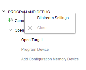
Figure 3.5 Bit file generation setting
-
-
- Click Bitstream setting, tick bin_file*, click OK. See Figure 3.6.
-
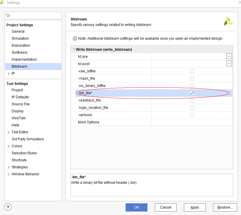
Figure 3.6 Bin file generation setting
-
-
- See Figure 3.7, click Generate Bitstream to generate the bit file and bin file. Click Open Hardware Manager to connect the board
-
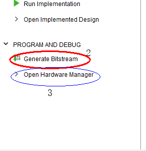
Figure 3.7 Bit file generation
-
-
- Click Open target to connect with the board. See Figure 3.8.
-
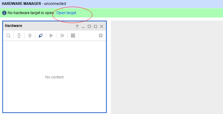
Figure 3.8 Connect to the develop board
- Select the chip in step 1, right click to choose Add Configuration Memory Device in step 2. See Figure 3.9.
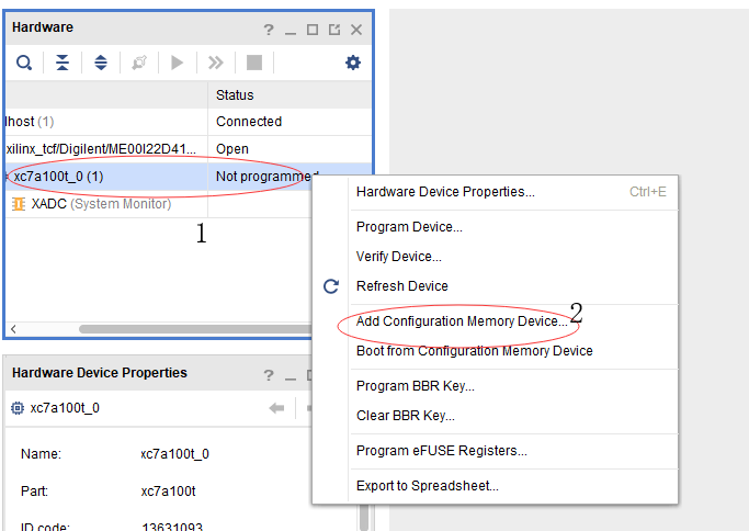
Figure 3.9 Adding memory device
- Choose the Flash chip to be mt25ql128, then click OK. See Figure 3.10.
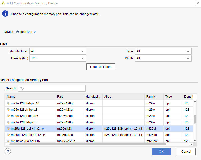
Figure 3.10 Select Flash part
- Add bin file to be the Configuration file.
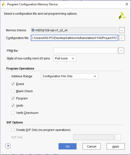
Figure 3.11 Add the bin file
- The test result is shown in Figure 3.12.
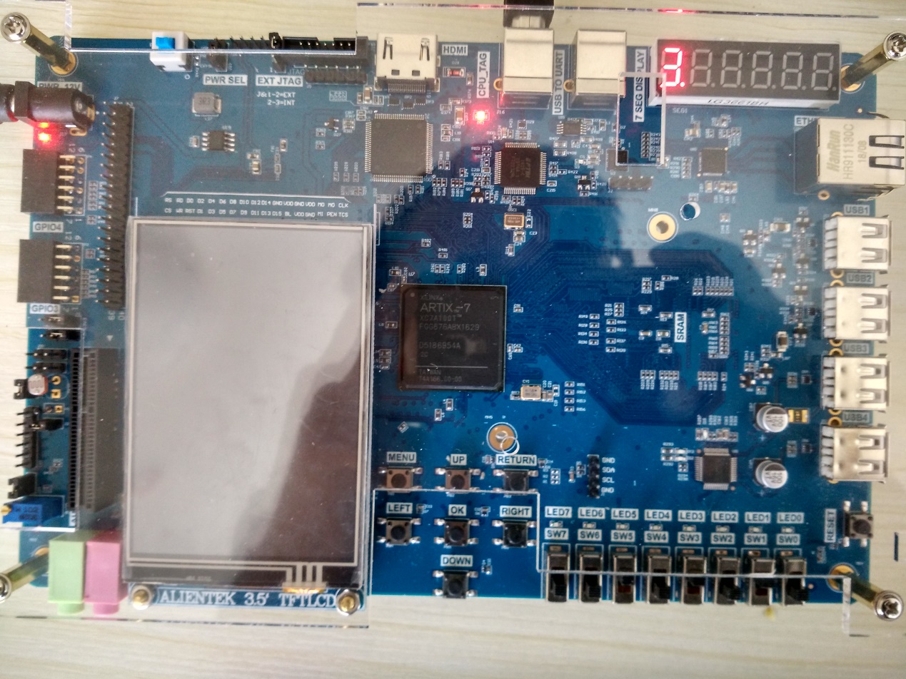
Figure 3.12 Test result
Experiment 4 Block/SCH Digital Clock Design
1.Experiment Objective
-
- Review the new FPGA project building in Vivado, device selection, PLL creation, PLL frequency setting, Verilog tree hierarchy design, and the use of ILA
- Master the design method of graphics from top to bottom
- Combine the BCD_counter project to realize the movement of the decimal point (DP) of the decoder
- Observe the test result
2.Experiment Procedure
- File -> Project -> New
Select Device: XC7A100T-2FGG676I
- See Figure 4.1, add source file, new top-level entity: block_counter.v
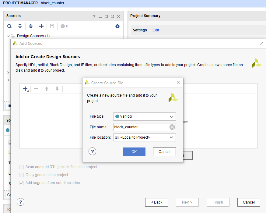
Figure 4.1 Build source file
- As shown in Figure 4.2, add the PLL as in the experiment 1, set the input clock to 50 MHz, and the output clock to 100 MHz.
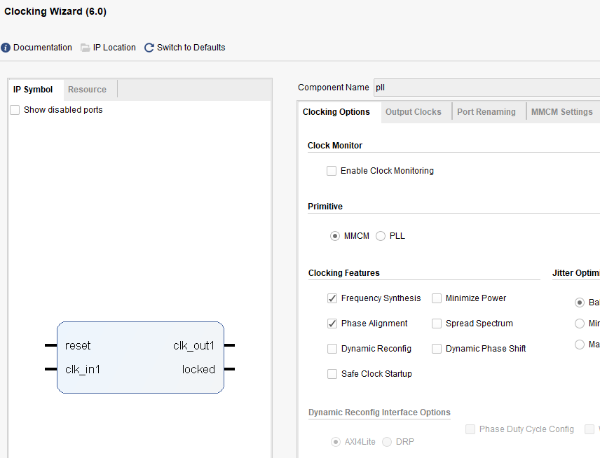
Figure 4.2 Set the PLL IP core
- Create a new Verilog HDL file for the frequency divider
- Divide the 100 MHz clock into a 1 MHz clock
|
-
- Create a new 1000 division verilog HDL file again, div_1000f.v
|
- Use the 1000 frequency division program div_1000f.v to divide the 1 MHZ clock into 1000 HZ, 1 HZ clock.
|
- Create a new Verilog file bcd_counter.v, design hour counter and minute counter
| module bcd_counter(
input rst, input sys_rst, input sys_clk, input ms_f, input s_f, output reg [7:0] seven_seg, output reg [3:0] scan ); reg ext_rst; reg min_f; reg [3:0] counta,countb; reg [3:0] countc,countd; reg [3:0] count_sel; reg [6:0]seven_seg_r; always@(posedge sys_clk) begin ext_rst<=sys_rst; end always@(posedge sys_clk) if(ext_rst)begin counta<=0; countb<=0; min_f <=1’b0; end else begin min_f <=1’b0; if(s_f) begin if(counta==4’d9) begin counta<=4’d0; if(countb==5)begin countb<=0; min_f<=1’b1; end else countb<=countb+1’b1; end else begin counta<=counta+1’b1; end end end always@(posedge sys_clk) if(ext_rst)begin countc<=4’d0; countd<=4’d0; end else begin if(min_f) begin if(countc==4’d9) begin countc<=4’d0; if(countd==5)begin countd<=0; end else countd<=countd+1’b1; end else begin countc<=countc+1’b1; end end end reg [1:0] scan_st; always@(posedge sys_clk) if(ext_rst) begin scan <=4’b1111; count_sel <=4’d0; scan_st<=0; end else case(scan_st) 0:begin scan <=4’b1110; count_sel <=counta; if(ms_f) scan_st <=1; end 1:begin scan <=4’b1101; count_sel <=countb; if(ms_f) scan_st <=2; end 2:begin scan<=4’b1011; count_sel <=countc; if(ms_f) scan_st<=3; end 3:begin scan<=4’b0111; count_sel <=countd; if(ms_f) scan_st<=0; end default:scan_st<=0; endcase always@(*) case(count_sel) 0:seven_seg_r<=7’b100_0000; 1:seven_seg_r<=7’b111_1001; 2:seven_seg_r<=7’b010_0100; 3:seven_seg_r<=7’b011_0000; 4:seven_seg_r<=7’b001_1001; 5:seven_seg_r<=7’b001_0010; 6:seven_seg_r<=7’b000_0011; 7:seven_seg_r<=7’b111_1000; 8:seven_seg_r<=7’b000_0000; 9:seven_seg_r<=7’b001_0000; default:seven_seg_r<=7’b100_0000; endcase always@(posedge sys_clk) seven_seg<={1’b1,seven_seg_r}; endmodule |
- Instantiate each function module subroutine into the top-level entity for comprehensive compilation.
|
- Lock the Pin
| Signal Name | Port Description | Network Label | FPGA Pin |
| inclk_in | Sytem clock 50 MHz | C10_50MCLK | U22 |
| rst | Reset, high by default | KEY1 | M4 |
| seven_seg[0] | Segment a | SEG_PA | K26 |
| seven_seg[1] | Segment b | SEG_PB | M20 |
| seven_seg[2] | Segment c | SEG_PC | L20 |
| seven_seg[3] | Segment d | SEG_PD | N21 |
| seven_seg[4] | Segment e | SEG_PE | N22 |
| seven_seg[5] | Segment f | SEG_PF | P21 |
| seven_seg[6] | Segment g | SEG_PG | P23 |
| seven_seg[7] | Segment h | SEG_DP | P24 |
| scan[0] | Segment 6 | SEG_3V3_D5 | T24 |
| scan[1] | Segment 5 | SEG_3V3_D4 | R25 |
| scan[2] | Segment 4 | SEG_3V3_D3 | K25 |
| scan[3] | Segment 3 | SEG_3V3_D2 | N18 |
- Compile, download to the board and test the program. The test result is shown in Figure 4.3.
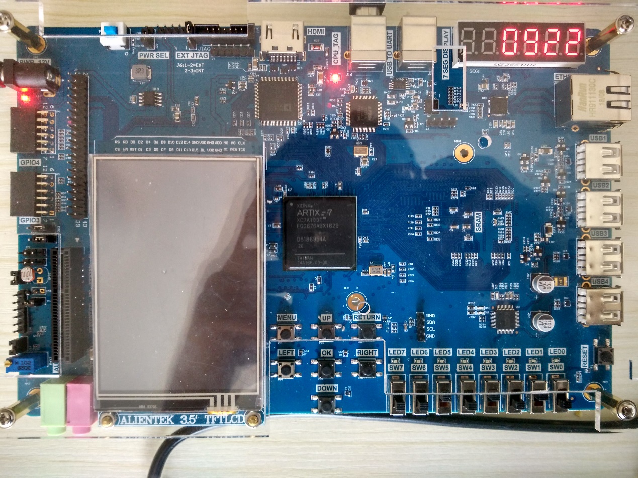
Figure 4.3 Test result
3.More to Practice
-
-
- Practice the design of high-level digital clocks, month (positional system by base 30), day (positional system by base 24), hour (sexagesimal), and minute (sexagesimal).
- The content of this lab exercise is to use the design with a top-down design approach.
-
Experiment 5 Button Debounce Design and Experimental Experiment
1.Experiment Objective
-
- Review the design of blinking LED
- Learn the principle of button debounce, and adaptive programming
- Learn the connection and use of the FII-PRX100T button schematics
- Integrated application of button debounce and another compatible program design
2.Experiment
- Button debounce principle
Usually, the switches used for the buttons are mechanical elastic switches. When the mechanical contacts are opened and closed, due to the elastic action of the mechanical contacts, a push button switch does not immediately turn on when closed, nor is it off when disconnected. Instead, there is some bouncing when connecting and disconnecting. See Figure 5.1
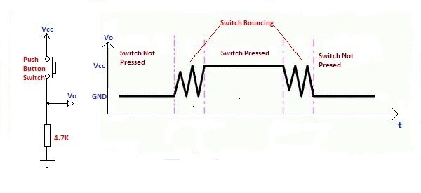
Figure 5.1 Button bounce principle
The length of the button’s stable closing time is determined by the operator. It usually takes more than 100ms. If you press it quickly, it will reach 40-50ms. It is difficult to make it even shorter. The bouncing time is determined by the mechanical characteristics of the button. It is usually between a few milliseconds and tens of milliseconds. To ensure that the program responds to the button’s every on and off, it must be debounced. When the change of the button state is detected, it should not be immediately responding to the action, but waiting for the closure or the disconnection to be stabilized before processing. Button debounce can be divided into hardware debounce and software debounce.
In most of cases, we use software or programs to achieve debounce. The simplest debounce principle is to wait for a delay time of about 10ms after detecting the change of the button state, and then perform the button state detection again after the bounce disappears. If the state is the same as the previous state just detected, the button can be confirmed. The action has been stabilized. This type of detection is widely used in traditional software design. However, as the number of button usage increases, or the buttons of different qualities will react differently. If the delay is too short, the bounce cannot be filtered out. When the delay is too long, it affects the sensitivity of the button.
This chapter introduces an adaptive button debounce method: starts timing when a change in the state of the button is detected. If the state changes within 10ms, the button bouncing exists. It returns to the initial state, clears the delay counter, and re-detects the button state until the delay counter counts to 10ms. The same debounce method is used for pressing and releasing the button. The flow chart is shown in Figure 5.2.
- Code for button debouncing
Verilog code is as follows:
|
Case 0 and 1 debounce the button press state. Case 2 and 3 debounce the button release state. After finishing the whole debounce procedure, the program outputs a synchronized clock pulse.
- Button debounce flow chart
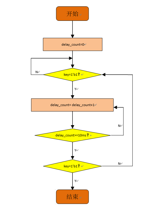
End
Start
Figure 5.2 Button debounce flow chart
- Combine running LED design and modify the button debounce.
- Build new project
- Create a PLL symbol
- Create a button debounce symbol (See the Verilog HDL code in this experiment)
- Create a top-level file key_filter
|
3.Hardware Design
- Button schematics
Figure 5.4 Button schematics
- FPGA pin mapping
| Signal Name | Port Description | Network Label | FPGA Pin |
| inclk_in | System clock 50 MHz | C10_50MCLK | U22 |
| rst | Reset, high by default | KEY1 | M4 |
| led0 | LED 0 | LED0 | N17 |
| led1 | LED 1 | LED1 | M19 |
| led2 | LED 2 | LED2 | P16 |
| led3 | LED 3 | LED3 | N16 |
| led4 | LED 4 | LED4 | N19 |
| led5 | LED 5 | LED5 | P19 |
| led6 | LED 6 | LED6 | N24 |
| led7 | LED 7 | LED7 | N23 |
| left | Press left | KEY4 | K5 |
| right | Press right | KEY6 | P1 |
-
- Compile and debug
- Download the program to the board and observe the test result. See Figure 5.5
Figure 5.5 Test Result
- Observe the test results. By default, 8 LEDs are off. Press the left button to switch the flow mode on the left side of the LED. Press the right button on the right side of the LED to switch between the flow mode. While holding down the left and right buttons, the LED remains in its original state.
Experiment 6 Digital Clock Comprehensive Design Experiment
1.Experiment Objective
-
- Design month, day, hour, minute, and second digital clock experiments, using 6 segment decoders
-
-
- 60 seconds carried to the minute
- 60 minutes carried to the hour
- 24 hours carried to the day
- 30 days carried to the month, and reset all
-
-
- Set four keys: menu, left, up, down
- The menu key controls the calibration function to switch between clock, date, and alarm.
- The left key selects which value is currently calibrated
- The Up and down keys add 1 and subtract 1 calibration to the data to be calibrated requires that the corresponding segment decoder is flashed.
- Modulate the design so that it can be reused
- Learn to use the module parameters
- Learn to use the timing analysis function of Vivado and correctly constrain the clock signal
- Design month, day, hour, minute, and second digital clock experiments, using 6 segment decoders
2.Design Procedure
- Build new project
-
- Project name is calendar_counter
- Select the device XC7A100TFGG676-2
- The top-level entity is calendar_counter.bdf or calendar_counter.v (Here the Verilog file is used)
-
- Design and integrate of submodule
-
- PLL module
- Frequency divider
- Button debounce module
- Counting module dual_num_count.v
-
Design a universal 2-bit counter that uses the parameter to specify the specified count setting.
|
- Button debounce
|
- Top-level entity design
|
- Lock the Pins
| Signal Name | Port Description | Network Label | FPGA Pin |
| inclk | System clock, 50 MHz | C10_50MCLK | U22 |
| rst | Reset, high by default | KEY1 | M4 |
| seven_seg[0] | Segment a | SEG_PA | K26 |
| seven_seg[1] | Segment b | SEG_PB | M20 |
| seven_seg[2] | Segment c | SEG_PC | L20 |
| seven_seg[3] | Segment d | SEG_PD | N21 |
| seven_seg[4] | Segment e | SEG_PE | N22 |
| seven_seg[5] | Segment f | SEG_PF | P21 |
| seven_seg[6] | Segment g | SEG_PG | P23 |
| seven_seg[7] | Segment h | SEG_DP | P24 |
| scan[0] | Segment 6 | SEG_3V3_D5 | T24 |
| scan[1] | Segment 5 | SEG_3V3_D4 | R25 |
| scan[2] | Segment 4 | SEG_3V3_D3 | K25 |
| scan[3] | Segment 3 | SEG_3V3_D2 | N18 |
| scan[4] | Segment 2 | SEG_3V3_D1 | R17 |
| scan[5] | Segment 1 | SEG_3V3_D0 | R16 |
| left | Left button | KEY4 | K5 |
| right | Right button | KEY6 | P1 |
| up | Up button | KEY2 | L4 |
| down | Bottom button | KEY2 | R7 |
- Compile
- Download the program to the develop board for verification
-
- Observe the test result
- Use the left, right keys to move the decimal point of the segment decoder
- Use up, down keys to calibrate time
-
The test result is shown in Figure 6.1, displaying time 10:27:05
Figure 6.1 Test result
3.Create an XDC File to Constrain the Clock
- Create constrain file
Figure 6.2 Craete SDC file
XDC file is as follows:
# Create Clock
create_clock -period 20 -name inclk -waveform {0.000 10.000} [get_ports inclk]
- Improve the precision when using up, down to calibrate
-
- The maximum value is automatic recognized, such as in the sexagesimal decimal digit calibration time, if the value reaches 5, the next Up will make the value become 0. When the timing of Down is reduced to 0, the next Down pulse will automatically change to 5.
- Compile, and download the program to the develop board
- Program to the flash memory
-
Experiment 7 Multiplier Use and ISIM Simulation
1.Experiment Objective
-
- Learn to use multiplier
- Use ISIM to simulate design output
2.Experiment Design
-
- Build new project mult_sim
-
-
- Select device XC7A100TFGG676-2
-
-
- Design implement
- 8×8 multiplier, the first input value is an 8-bit switch, and the second input value is the output of an 8-bit counter.
- Observe the result on Modelsim
- Observe the result on 6 segment decoders
- Design procedure
- Create new file mult_sim.v
- Add PLL,set the input clock to be 50 MHz, and the output clock to be 100 MHz
- Add LPM_MULT IP
- Build new project mult_sim
IP Catalog -> input Mult in the search box. Invoke the multipliers. See Figure 7.1.
Figure 7.1 Build IP core for multiplier
-
-
- Choose input data type to be unsigned and width to be 8. See Figure 7.2.
-
Figure 7.2 Set the input data type and data width
-
-
- Choose Pipelining and Control Signals. See Figure 7.3. Add a delay of 1 stage. The default optimum stage is 3 stages.
-
Figure 7.3 Pipelining setting
-
- Choose default for other settings
- Instantiate in the top-level entity
3.The Top-level Entity Is as Follows:
|
4.ISIM Simulation Library Compilation and Call
Under the Vivado platform, you can choose to use built-in simulation tool ISIM or third-party simulation tools for functional simulation of the project. Simulating with the Modelsim simulation tool requires a separate compilation of the simulation library. This routine uses the built-in ISIM tool emulation and briefly introduce Modelsim’s Xilinx simulation library file compilation for simulation using Modelsim.
- Build simulation project files.
Add the testbench file under Simulation Sources. See Figure 7.4.
Figure 7.4 Add the testbench file
Simulation testbench code is as follows:
|
- As shown in Figure 7.5, after the simulation stimulus file is added, ISIM can be started in Simulation->Run Simulation –> Run Behavioral Simulation on the left side of the project management.
Figure 7.5 Simulation library compiled
- Simulation result is shown in Figure 7.6.
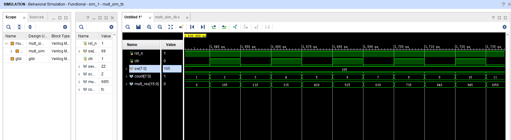
Figure 7.6 Simulation result
- Compile ModelSim library
After installing ModelSim, compile the Xilinx simulation library file first. The specific process is as follows:
-
-
- Tools -> Compile Simulation Libraries. See Figure 7.7 for the popup window.
-
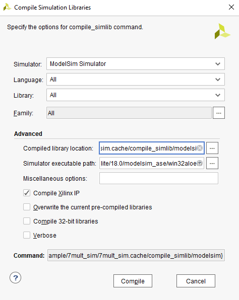
Figure 7.7 Compilation library address setting
-
-
- As shown in Figure 7.8, the compilation is completed. Note that the process is very time consuming.
-
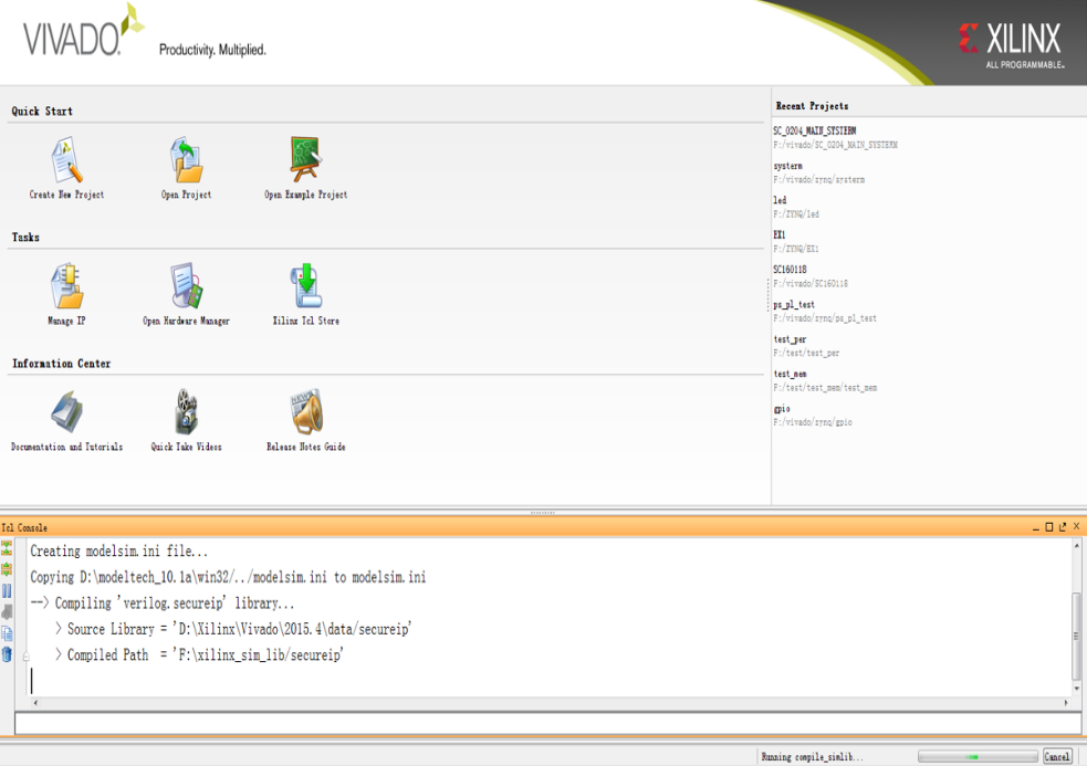
Figure 7.8 Simulation library compiled
Approachable advanced information for ModelSim can be referred online. Here would not go into more details.
- More to practice
- Design an 8-bit trigger, simulate with Modelsim
- Learn to write testbenches for simulation
Experiment 8 Hexadecimal Number to BCD Code Conversion and Application
1.Experiment Objective
-
- Since the hexadecimal display is not intuitive, decimal display is more widely used in real life.
- Human eye recognition is relatively slow, so the display from hexadecimal to decimal does not need to be too fast. Generally, there are two methods
- Countdown method: Under the control of the synchronous clock, the hexadecimal number is decremented by 1 until it is reduced to 0. At the same time, the appropriate BCD code decimal counter is designed to increment. When the hexadecimal number is reduced to 0, the BCD counter just gets with the same value to display.
- Bitwise operations (specifically, shift bits and plus 3 here). The implementation is as follows:
- Set the maximum decimal value of the expression. Suppose you want to convert the 16-digit binary value (4-digit hexadecimal) to decimal. The maximum value can be expressed as 65535. First define five four-digit binary units: ten thousand, thousand, hundred, ten, and one to accommodate calculation results
- Shift the hexadecimal number by one to the left, and put the removed part into the defined variable, and judge whether the units of ten thousand, thousand, hundred, ten, and one are greater than or equal to 5, and if so, add the corresponding bit to 3 until the 16-bit shift is completed, and the corresponding result is obtained.
Note: Do not add 3 when moving to the last digit, put the operation result directly
-
-
-
- The Principle of hexadecimal number to BCD number conversion
-
-
Suppose ABCD is a 4-digit binary number (possibly ones, 10 or 100 bits, etc.), adjusts it to BCD code. Since the entire calculation is implemented in successive shifts, ABCDE is obtained after shifting one bit (E is from low displacement and its value is either 0 or 1). At this time, it should be judged whether the value is greater than or equal to 10. If so, the value is increased by 6 to adjust it to within 10, and the carry is shifted to the upper 4-bit BCD code. Here, the pre-movement adjustment is used to first determine whether ABCD is greater than or equal to 5 (half of 10), and if it is greater than 5, add 3 (half of 6) and then shift.
For example, ABCD = 0110 (decimal 6)
- After shifting it becomes 1100 (12), greater than 1001 (decimal 9)
- By plus 0110 (decimal 6), ABCD = 0010, carry position is 1, the result is expressed as decimal
- Use pre-shift processing, ABCD = 0110 (6), greater than 5, plus 3
- ABCD=1001(9), shift left by one
- ABCD=0010, the shifted shift is the lowest bit of the high four-bit BCD.
- Since the shifted bit is 1, ABCD = 0010(2), the result is also 12 in decimal
- The two results are the same
- Firstly, make a judgement, and then add 3 and shift. If there are multiple BCD codes at the same time, then multiple BCD numbers all must first determine whether need to add 2 and then shift.
- The first way is relatively easy. Here, the second method is mainly introduced.
Example 1:
Figure 8.1 Binary to decimal
Example 2:
Figure 8.2 Hex to BCD
-
- Write a Verilog HDL to convert 16-bit binary to BCD. (You can find reference in the project folder, HEX_BCD.v
|
-
- Modelsim simulation
- Refer to last experiment for setting Modelsim
- Simulation result shown in Figure 8.3.
- Modelsim simulation
Figure 8.3 Simulation result for Hex to BCD
-
- Remark
The assignment marks for the examples above are “=” instead of “<=”. Why?
Since the whole program is designed to be combinational logic, when invoking the modules, the other modules should be synchronized the timing.
2.Application of Hexadecimal Number to BCD Number Conversion
- Continue to complete the multiplier of experiment 7 and display the result in segment decoders in decimal. The code is as follows:
| module mult_sim(
input rst, input inclk, input [7:0] sw, output reg[6:0] seven_sega, output reg[5:0] scan ); wire [15:0] mult_res; wire sys_clk; wire sys_rst; wire us_f; wire ms_f; wire s_f; reg [7:0] count; reg [3:0] counta; reg [6:0] seven_seg_ra; wire [3:0] ones; wire [3:0] tens; wire [3:0] hundreds; wire [3:0] thousands; wire [3:0] ten_thousands; reg [3:0] ones_r; reg [3:0] tens_r; reg [3:0] hundreds_r; reg [3:0] thousands_r; reg [3:0] ten_thousands_r; always@(posedge sys_clk) if(sys_rst) begin count <=0; ones_r <=0; tens_r <=0; hundreds_r<=0; thousands_r<=0; ten_thousands_r<=0; end else if(s_f) begin count<=count+1; ones_r <=ones; tens_r <=tens; hundreds_r<=hundreds; thousands_r<=thousands; ten_thousands_r<=ten_thousands; end reg ext_rst; always@(posedge sys_clk) ext_rst<=rst; reg [2:0] scan_st; always@(posedge sys_clk) if(!ext_rst) begin scan<=6’b11_1111; counta<=4’b0; scan_st<=0; end else case(scan_st) 0:begin scan<=6’b11_1110; counta<=ones_r; if(ms_f) scan_st<=1; end 1:begin scan<=6’b11_1101; counta<=tens_r; if(ms_f) scan_st<=2; end 2:begin scan<=6’b11_1011; counta<=hundreds_r; if(ms_f) scan_st<=3; end 3:begin scan<=6’b11_0111; counta<=thousands_r; if(ms_f) scan_st<=4; end 4:begin scan<=6’b10_1111; counta<=ten_thousands_r; if(ms_f) scan_st<=5; end 5:begin scan<=6’b01_1111; counta<=0; if(ms_f) scan_st<=0; end default:scan_st<=0; endcase always@(*) case(counta) 0:seven_seg_ra<=7’b100_0000; 1:seven_seg_ra<=7’b111_1001; 2:seven_seg_ra<=7’b010_0100; 3:seven_seg_ra<=7’b011_0000; 4:seven_seg_ra<=7’b001_1001; 5:seven_seg_ra<=7’b001_0010; 6:seven_seg_ra<=7’b000_0010; 7:seven_seg_ra<=7’b111_1000; 8:seven_seg_ra<=7’b000_0000; 9:seven_seg_ra<=7’b001_0000; default:seven_seg_ra<=7’b100_0000; endcase always@(posedge sys_clk) seven_sega<=seven_seg_ra; lpm_mult8x8 lpm_mult8x8_inst ( .CLK(inclk), // input wire CLK .A(sw), // input wire [7 : 0] A .B(count), // input wire [7 : 0] B .P(mult_res) // output wire [15 : 0] P ); pll_sys_rst pll_sys_rst_inst ( .clk_in (inclk), .sys_clk (sys_clk), .sys_rst (sys_rst), .BCD_clk ( ) ); us_ms_s_div us_ms_s_div_inst ( .sys_rst (sys_rst), .sys_clk (sys_clk), .us_f (us_f), .ms_f (ms_f), .s_f (s_f) ); HEX_BCD HEX_BCD_inst ( .hex (mult_res), .ones (ones), .tens (tens), .hundreds (hundreds), .thousands (thousands), .ten_thousands (ten_thousands) ); endmodule |
- After completing the implementation process, click Open Implementation Design as shown in Figure 8.4. Observe the Report Timing Summary and view the circuit timing report.
Figure 8.4 Timing report check
The result is shown in Figure 8.5.
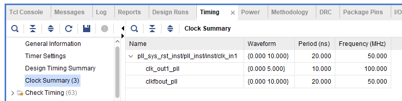
Figure 8.5 Timing report
It satisfies the timing requirement.
- Pin assignment
| Signal Name | Port Description | Network Label | FPGA Pin |
| inclk | System clock, 50 MHz | C10_50MCLK | U22 |
| rst | Reset, high by default | KEY1 | M4 |
| seven_sega[0] | Segment a | SEG_PA | K26 |
| seven_sega[1] | Segment b | SEG_PB | M20 |
| seven_sega[2] | Segment c | SEG_PC | L20 |
| seven_sega[3] | Segment d | SEG_PD | N21 |
| seven_sega[4] | Segment e | SEG_PE | N22 |
| seven_sega[5] | Segment f | SEG_PF | P21 |
| seven_sega[6] | Segment g | SEG_PG | P23 |
| seven_sega[7] | Segment h | SEG_DP | P24 |
| scan[0] | Segment 6 | SEG_3V3_D5 | T24 |
| scan[1] | Segment 5 | SEG_3V3_D4 | R25 |
| scan[2] | Segment 4 | SEG_3V3_D3 | K25 |
| scan[3] | Segment 3 | SEG_3V3_D2 | N18 |
| scan[4] | Segment 2 | SEG_3V3_D1 | R17 |
| scan[5] | Segment 1 | SEG_3V3_D0 | R16 |
| sw[0] | Swicth input | GPIO_DIP_SW0 | N8 |
| sw[1] | Swicth input | GPIO_DIP_SW1 | M5 |
| sw[2] | Swicth input | GPIO_DIP_SW2 | P4 |
| sw[3] | Swicth input | GPIO_DIP_SW3 | N4 |
| sw[4] | Swicth input | GPIO_DIP_SW4 | U6 |
| sw[5] | Swicth input | GPIO_DIP_SW5 | U5 |
| sw[6] | Swicth input | GPIO_DIP_SW6 | R8 |
| sw[7] | Swicth input | GPIO_DIP_SW7 | P8 |
- Compile, and download the program to the board. The test result is shown below:
Figure 8.6 Hex to BCD result
3.Experiment Reflection
-
- How to implement BCD using more than 16 bits binary numbers
- How to handle an asynchronous clock
- Learn how to design circuits that meet timing requirements based on actual needs
Experiment 9 Use of ROM
1.Experiment Objective
- Study the internal memory block of FPGA
- Study the format of *.coe and how to edit *.coe file to configure the contents of ROM
- Learn to use RAM, read and write RAM
2.Experiment Design
-
- Design 16 outputs ROM, address ranging 0-255
- Interface 8-bit switch input as ROM’s address
- Segment decoders display the contents of ROM and require conversion of hexadecimal to BCD output.
3.Design Procedure
- Create a coe file. This experiment *.coe file is generated based on Matlab2018. The *.m file is as follows:
|
- *.coe file syntax is shown in Figure 9.1.
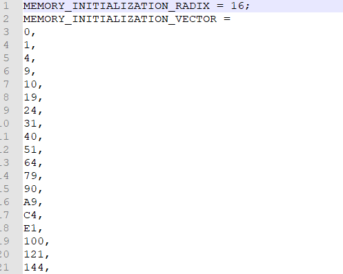
Figure 9.1 *.coe file syntax
- Create new project, rom_test, select device XC7A100TFGG676-2
- Click IP Catalog, and input ROM in the search box. Choose Block Memory Generator. See Figure 9.2.
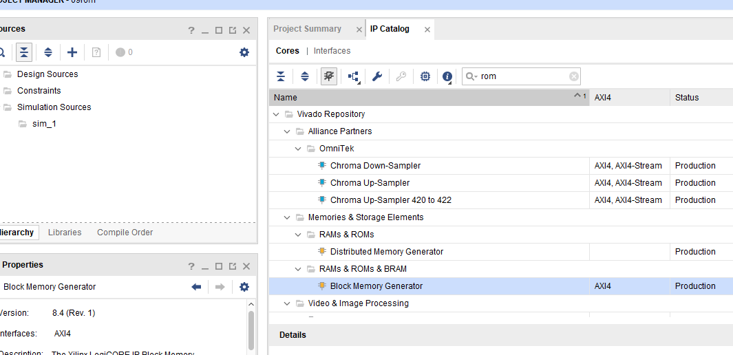
Figure 9.2 Use of ROM IP core
- Select the memory type be Single Port ROM. See Figure 9.3.
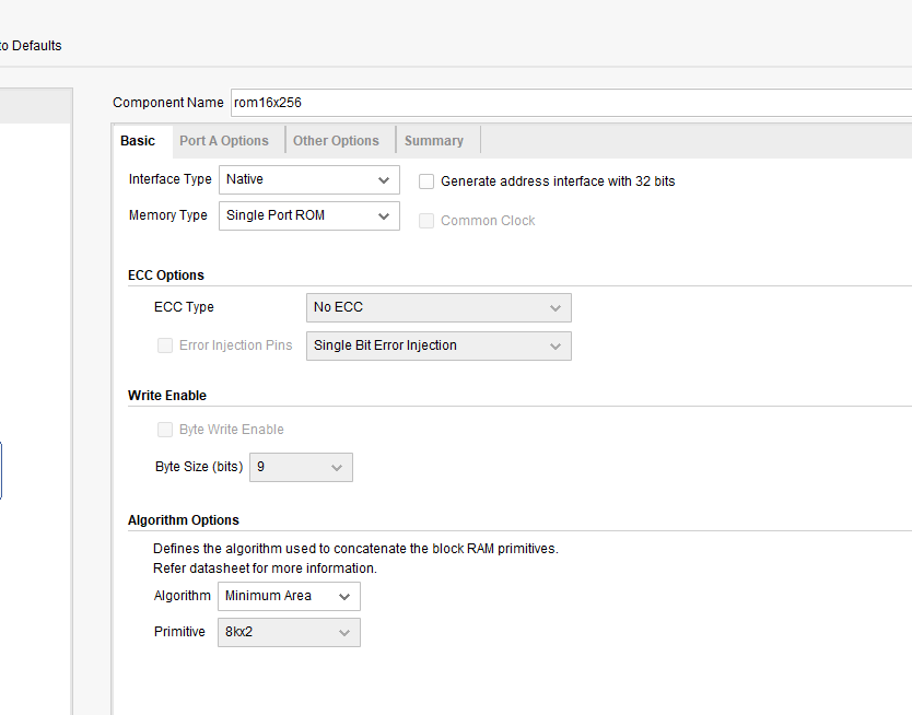
Figure 9.3 Memory type selection
- Click Port A Options tag. Set as shown in Figure 9.4.
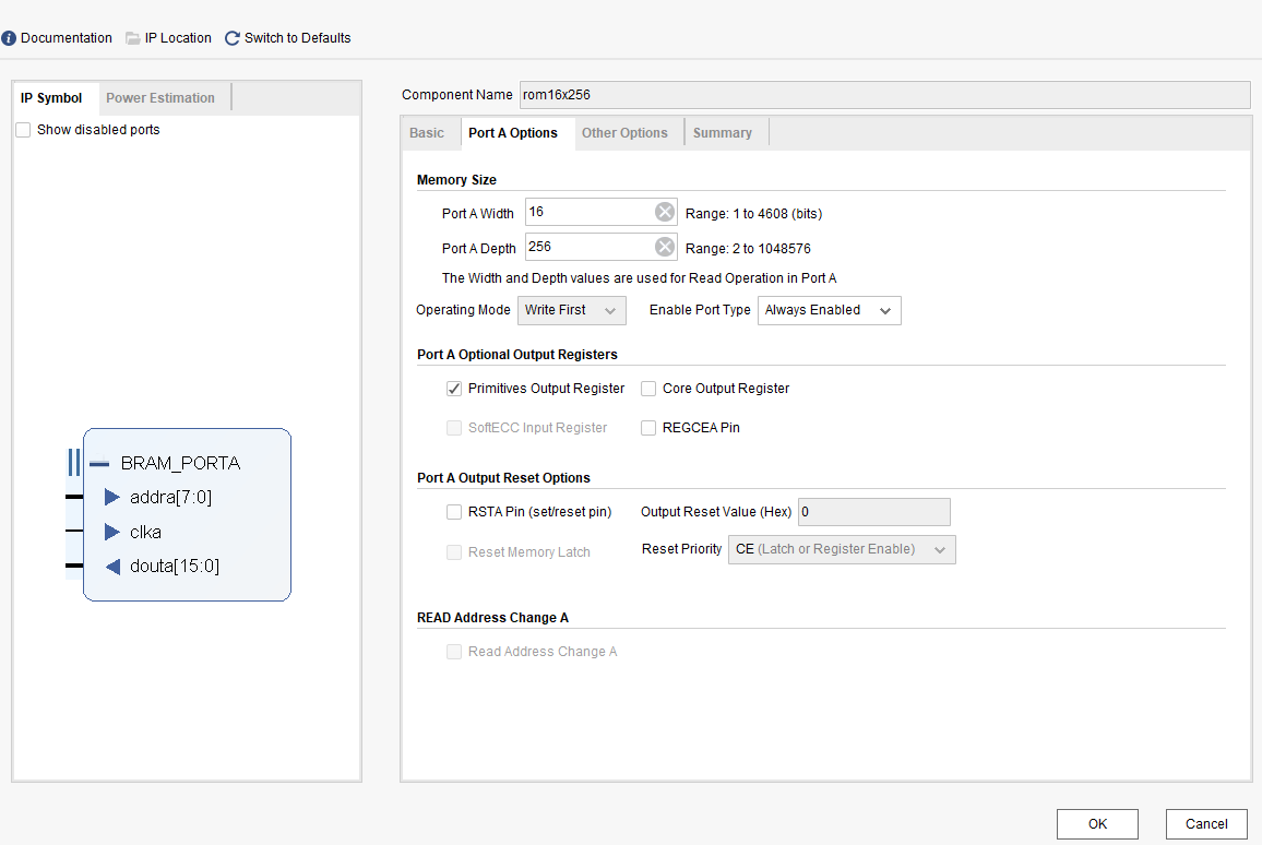
Figure 9.4 Port memory width setting
- Click the Other Options tab shown in Figure 9.5, select the Load Init File check box, set the correct *.coe file location, and initialize the rom.
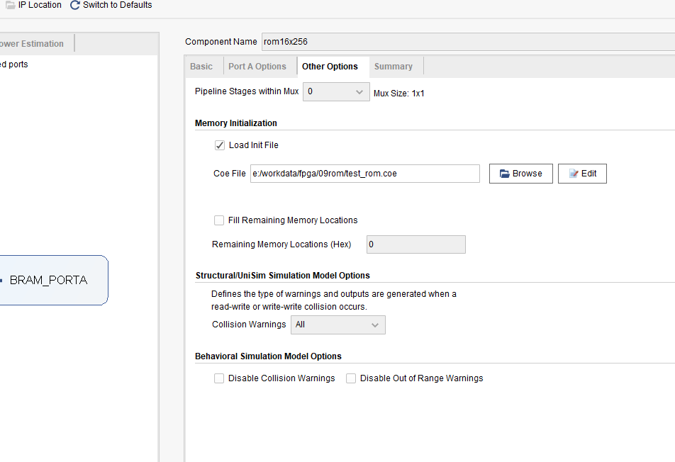
Figure 9.5 ROM initialization
- Set others as default
- Click OK to finish setting for IP core. Generate other files related as default setting.
- Create top-level entity, rom_test.v
- Add PLL (Input clock 50 MHz, output clock 100 MHz)
- Add us_ms_s_div.v and instantiate it. Refer previous experiments for more
- Add HEX_BCD and instantiate it
- The code is given below:
|
-
- Compile
- Lock the pins
| Signal Name | Port Description | Network Label | FPGA Pin |
| inclk | Sytem clock, 50 MHz | C10_50MCLK | U22 |
| rst | Reset, hight by default | KEY1 | M4 |
| seven_sega[0] | Segment a | SEG_PA | K26 |
| seven_sega[1] | Segment b | SEG_PB | M20 |
| seven_sega[2] | Segment c | SEG_PC | L20 |
| seven_sega[3] | Segment d | SEG_PD | N21 |
| seven_sega[4] | Segment e | SEG_PE | N22 |
| seven_sega[5] | Segment f | SEG_PF | P21 |
| seven_sega[6] | Segment g | SEG_PG | P23 |
| seven_sega[7] | Segment h | SEG_DP | P24 |
| scan[0] | Segment 6 | SEG_3V3_D5 | T24 |
| scan[1] | Segment 5 | SEG_3V3_D4 | R25 |
| scan[2] | Segment 4 | SEG_3V3_D3 | K25 |
| scan[3] | Segment 3 | SEG_3V3_D2 | N18 |
| scan[4] | Segment 2 | SEG_3V3_D1 | R17 |
| scan[5] | Segment 1 | SEG_3V3_D0 | R16 |
| sw[0] | Switch input | GPIO_DIP_SW0 | N8 |
| sw[1] | Switch input | GPIO_DIP_SW1 | M5 |
| sw[2] | Switch input | GPIO_DIP_SW2 | P4 |
| sw[3] | Switch input | GPIO_DIP_SW3 | N4 |
| sw[4] | Switch input | GPIO_DIP_SW4 | U6 |
| sw[5] | Switch input | GPIO_DIP_SW5 | U5 |
| sw[6] | Switch input | GPIO_DIP_SW6 | R8 |
| sw[7] | Switch input | GPIO_DIP_SW7 | P8 |
-
- Download the program and test the result
Figure 9.6 Test result
- Experiment summary and reflection
- How to use the initial file of ROM to realize the decoding, such as decoding and scanning the segment decoders.
- Write a *.mif file to generate sine, cosine wave, and other function generators.
- Comprehend application, combine the characteristic of ROM and PWM to form SPWM modulation waveform.
Experiment 10 Use Dual_port RAM to Read and Write Frame Data
1.Experiment Objective
-
- Learn to configure and use dual-port RAM
- Learn to use synchronous clock to control the synchronization of frame structure
- Learn to use asynchronous clock to control the synchronization of frame structure
- Use ILA to observe the structure of a synchronized clock frame
- Extended the use of dual-port RAM
- Design the use of three-stage state machine
2.Experiment Implement
- Generate dual-port RAM and PLL
- 16-bit width, 256-depth dual-port RAM
- 2 PLL, both 50 MHz input, different 100 MHz and 20 MHz outputs
- Design a 16-bit data frame
- Data is generated by an 8-bit counter: Data={~counta,counta}
- The ID of the data frame inputted by the switch (7 bits express maximum of 128 different data frames)
- 16-bit checksum provides data verification
-
-
- 16-bit checksum accumulates, discarding the carry bit
- After the checksum is complemented, append to the frame data
-
-
- Provide configurable data length data_len by parameter
- Packet: When the data and checksum package are written to the dual-port RAM, the userID, the frame length and the valid flag are written to the specific location of the dual-port RAM. The structure of the memory is shown below
| Wr_addr | Date/ Flag | Rd_addr |
| 8’hff | {valid, ID, data_len} | 8’hff |
| … | N/A | … |
| 8’hnn+2 | N/A | 8’hnn+2 |
| 8’hnn+1 | ~checksum+1 | 8’hnn+1 |
| 8’hnn | datann | 8’hnn |
| … | …. | … |
| 8’h01 | Data1 | 8’h01 |
| 8’h00 | Data0 | 8’h00 |
- Read and write in an agreed order
Firstly, write in the order
- Read the flag of the 8’hff address (control word). If valid=1’b0, the program proceeds to the next step, otherwise waits
- Address plus 1, 8’hff+1 is exactly zero, write data from 0 address and calculate the checksum
- Determine whether the interpretation reaches the predetermined data length. If so, proceeds to next step, otherwise the data is written, and the checksum is calculated.
- checksum complements and write to memory
- Write the control word in the address 8’hff, packet it
Secondly, read in the order
- Idle is the state after reset
- Init: Initialization, set the address to 8’hff
- Rd_pipe0: Add a latency (since the read address and data are both latched). Address +1, forming a pipeline structure
- Read0: Set the address to 8’hff, read the control word and judge whether the valid bit is valid.
If valid=1’b1, address +1, proceeds to the next step
If valid=1’b0, it means the packet is not ready yet, the address is set to be 8’hff and returns to the init state.
- Read1: Read the control word again
If valid=1’b1, address+1, ID and data length are assigned to the corresponding variables and proceeds to the next step
If valid=1’b0, it means the packet is not ready yet, the address is set to 8’hff, and returns to the init state.
- Rd_data:
Read data and pass to data variables
Calculate checksum, data_len – 1
Determine whether the data_len is 0, if so, all data has been read, proceeds to the next step, otherwise, continue the operation in current state
- grd_chsum: Read the value of checksum and calculate the last checksum. Correct the data and set the flag of rd_err
- rd_done: The last step clears the valid flag in memory and opens the write enable for the next packet.
Thirdly, valid is the handshake signal. This flag provides the possibility of read and write synchronization, so the accuracy of this signal must be ensured in the program design. See the project files for more details.
3.Program Design
-
- Port
module frame_ram
#(parameter data_len=250)
(
input inclk,
input rst, //external reset
input [6:0] sw, //used as input ID
output reg[6:0] oID, //used as output ID
output reg rd_done, //frame read is done
output reg rd_err //frame read has errors
);
-
- Definition of state machine
parameter [2:0] mema_idle=0,
mema_init=1,
mema_pipe0=2,
mema_read0=3,
mema_read1=4,
mema_wr_data=5,
mema_wr_chsum=6,
mema_wr_done=7;
parameter [2:0] memb_idle=0,
memb_init=1,
memb_pipe0=2,
memb_read0=3,
memb_read1=4,
memb_rd_data=5,
memb_rd_chsum=6,
memb_rd_done=7;
-
- Define clock parameter
wire sys_clk;
wire BCD_clk;
wire sys_rst;
reg ext_clk;
-
- Define two-port RAM interface
reg [7:0] addr_a;
reg [15:0] data_a;
reg wren_a;
wire [15:0] q_a;
reg [7:0] addr_b;
reg wren_b;
wire [15:0] q_b;
-
- Write state machine partial variable definition
- Write stste machine variables
- Write state machine partial variable definition
reg[6:0] user_id;
reg[7:0] wr_len;
reg[15:0] wr_chsum;
Wire wr_done;
reg[7:0] counta;
Wire[7:0] countb=~counta;
Reg ext_rst;
Reg [2:0] sta;
reg[2:0] sta_nxt;
-
-
- Read state machine variables
-
reg[15:0] rd_chsum;
reg[7:0] rd_len;
reg[15:0] rd_data;
Reg ext_rst;
reg[2:0] stb;
reg[2:0] stb_nxt;
-
- Data generation counter
always@(posedge BCD_clk)
ext_rst<=rst;
always@(posedge sys_clk)
if(sys_rst) begin
counta <=0;
user_id <=0;
end
else begin
counta <=counta+1;
user_id<=sw;
End
-
- Write state machine
- First and second stages
- Write state machine
assign wr_done=(wr_len==data_len-1);//Think why using wr_len==data_len-1
//instead of wr_len==data_len
always@(posedge sys_clk)
if(sys_rst) begin
sta=mema_idle;
end
else
sta=sta_nxt;
always@(*)
case (sta)
mema_idle : sta_nxt=mema_init;
mema_init : sta_nxt=mema_pipe0;
mema_pipe0 : sta_nxt=mema_read0;
mema_read0 :begin
if(!q_a[15])
sta_nxt=mema_read1;
else
sta_nxt=sta;
end
mema_read1:begin
if(!q_a[15])
sta_nxt=mema_wr_data;
else
sta_nxt=sta;
end
mema_wr_data: begin
if(wr_done)
sta_nxt=mema_wr_chsum;
else
sta_nxt=sta;
end
mema_wr_chsum: sta_nxt=mema_wr_done;
mema_wr_done: sta_nxt=mema_init;
default:sta_nxt=mema_idle;
endcase
-
-
- Third stage
-
always@(posedge sys_clk)
case (sta)
mema_idle: begin
addr_a<=8’hff;
wren_a<=1’b0;
data_a<=16’b0;
wr_len<=8’b0;
wr_chsum<=0;
end
mema_init,mema_pipe0,mema_read0,mema_read1: begin
addr_a<=8’hff;
wren_a<=1’b0;
data_a<=16’b0;
wr_len<=8’b0;
wr_chsum<=0;
end
mema_wr_data:begin
addr_a<=addr_a+1;
wren_a<=1’b1;
data_a<={countb,counta};
wr_len<=wr_len+1;
wr_chsum<=wr_chsum+{countb,counta};
end
mema_wr_chsum:begin
addr_a<=addr_a+1;
wr_len<=wr_len+1;
wren_a<=1’b1;
data_a<=(~wr_chsum)+1’b1;
end
mema_wr_done:begin
addr_a<=8’hff;
wren_a<=1’b1;
data_a<={1’b1,user_id,wr_len};
end
default:;
endcase
-
- Read state machine
- First stage
- Read state machine
always@(posedge sys_clk)
if(!ext_rst) begin
stb=memb_idle;
end
else
stb=stb_nxt;
-
-
- Second stage
-
always@(*)
case (stb)
memb_idle : stb_nxt=memb_init;
memb_init : stb_nxt=memb_pipe0;
memb_pipe0 : stb_nxt=memb_read0;
memb_read0 :begin
if(q_b[15])
stb_nxt=memb_read1;
else
stb_nxt=memb_init;
end
memb_read1:begin
if(q_b[15])
stb_nxt=memb_rd_data;
else
stb_nxt=memb_init;
end
memb_rd_data: begin
if(rd_done)
stb_nxt=memb_rd_chsum;
else
stb_nxt=stb;
end
memb_rd_chsum: stb_nxt=memb_rd_done;
memb_rd_done: stb_nxt=memb_init;
default:stb_nxt=memb_idle;
endcase
-
-
- Third stage. The actual operation is driven by the edge of the clock
-
always@(posedge sys_clk)
case(stb)
memb_idle: begin
addr_b<=8’hff;
rd_data<=0;
rd_chsum<=0;
wren_b<=1’b0;
rd_len<=8’b0;
oID<=7’b0;
rd_err<=1’b0;
end
memb_init: begin
addr_b<=8’hff;
rd_data<=0;
rd_chsum<=0;
wren_b<=1’b0;
rd_len<=8’b0;
oID<=7’b0;
rd_err<=1’b0;
endmemb_pipe0: begin
addr_b<=8’b0;
end
memb_read0: begin
if(q_b[15])
addr_b<=addr_b+1’b1;
else
addr_b<=8’hff;
rd_data<=0;
rd_chsum<=0;
wren_b<=1’b0;
rd_len<=8’b0;
oID<=7’b0;
end
memb_read1: begin
if(q_b[15])
addr_b<=addr_b+1’b1;
else
addr_b<=8’hff;
rd_data<=0;
rd_chsum<=0;
wren_b<=1’b0;
rd_len<=q_b[7:0];
oID<=q_b[14:8];
end
memb_rd_data: begin
addr_b<=addr_b+1’b1;
rd_data<=q_b;
rd_chsum<=rd_chsum+rd_data;
wren_b<=1’b0;
rd_len<=rd_len-1’b1;
end
memb_rd_chsum: begin
addr_b<=8’hff;
wren_b<=1’b0;
if(!rd_chsum)//Determine if rd_chsum is not 0, else error occurs when reading data
rd_err<=1’b1;
end
memb_rd_done: begin
addr_b<=8’hff;
wren_b<=1’b1;
end
default:;
endcase
always@(*)begin
if(stb==memb_rd_data)
rd_done=(rd_len==0);
else
rd_done=1’b0;
end
-
- Instantiate dual_port RAM and PLL
//Instantiate dual-port RAM
dp_ram dp_ram_inst
(
.address_a(addr_a),
.address_b(addr_b),
.clock (sys_clk),
.data_a (data_a),
.data_b (16’b0),
.wren_a (wren_a),
.wren_b(wren_b),
.q_a (q_a),
.q_b (q_b)
);
//Instantiate PLL
pll_sys_rst pll_sys_rst_inst
(
.inclk (inclk),
.sys_clk (sys_clk),
.BCD_clk(BCD_clk),
.sys_rst (sys_rst)
);
endmodule
4.Lock the Pins, Compile, and Download to The Board to Test
- Pin assignment
| Signal Name | Port Description | Network Label | FPGA Pin |
| inclk | System clock, 50 MHz | C10_50MCLK | U22 |
| rst | Reset, high by default | KEY1 | M4 |
| oID_r[0] | LED 0 | LED0 | N17 |
| oID_r[1] | LED 1 | LED1 | M19 |
| oID _r[2] | LED 2 | LED2 | P16 |
| oID _r[3] | LED 3 | LED3 | N16 |
| oID _r[4] | LED 4 | LED4 | N19 |
| oID_r [5] | LED 5 | LED5 | P19 |
| oID_r [6] | LED 6 | LED6 | N24 |
| sw[0] | Switch input | GPIO_DIP_SW0 | N8 |
| sw[1] | Switch input | GPIO_DIP_SW1 | M5 |
| sw[2] | Switch input | GPIO_DIP_SW2 | P4 |
| sw[3] | Switch input | GPIO_DIP_SW3 | N4 |
| sw[4] | Switch input | GPIO_DIP_SW4 | U6 |
| sw[5] | Switch input | GPIO_DIP_SW5 | U5 |
| sw[6] | Switch input | GPIO_DIP_SW6 | R8 |
| rd_err_r | Read error flag | SEG_PA | P24 |
| rd_done_r | Dual-port end reading | SEG_PB | K26 |
| weixuan | Segment 1 | SEG_3V3_D0 | R16 |
- Download the program to the develop board
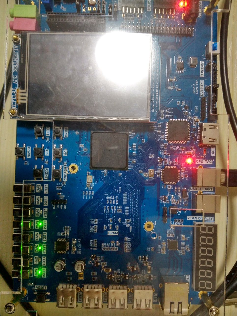
Figure 10.1 Dual_port RAM test result
From the test results, SW6~SW0 (write ID) and read ID (LEDs) are completely consistent. And no error reading occurred during the reading and writing process. The results can be derived from the ILA plot.
5.Use ILA to Observe Dual_port RAM Read and Write
- To facilitate the observation of the read and write state machine synergy results, the data length is changed to 4 here, recompile and download. Users can test themselves using long data.
module frame_ram
#(parameter data_len=4)
(
input inclk,
input rst, //external reset
input [6:0]sw, //used as input ID
output reg[6:0] oID, //used as output ID
output reg rd_done, //frame read is done
output reg rd_err //frame read has errors
);
- ILA test result. See Figure 10.2
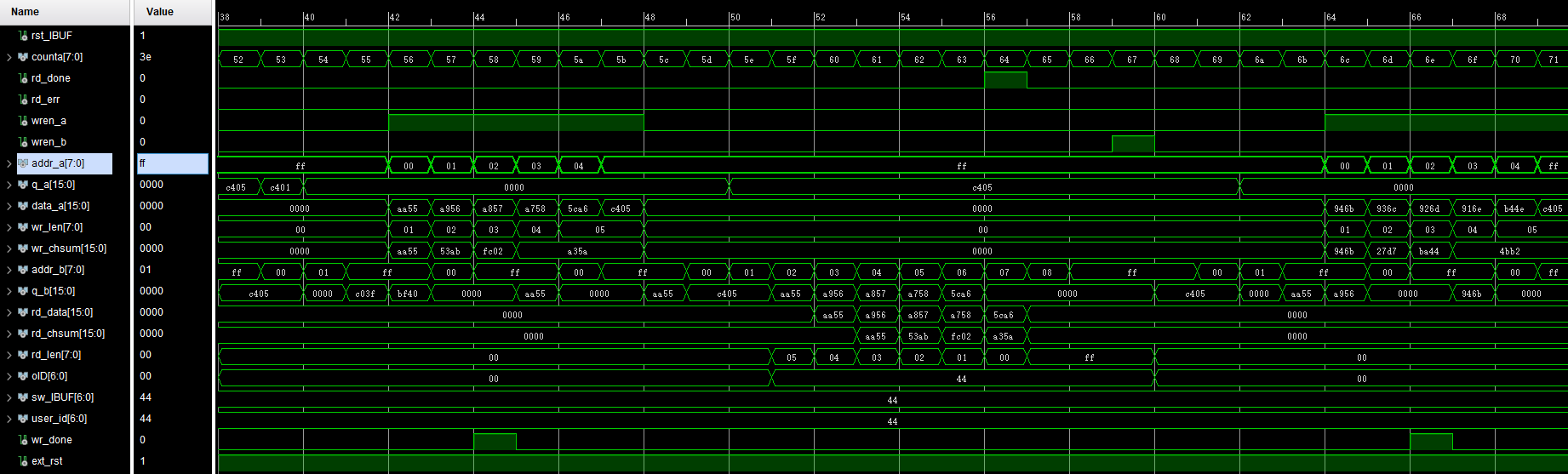
Figure 10.2 Signals observed form ILA
- Observe the test result
- Observe the handshake mechanism through dual-port RAM
Determine whether the reading is started after the packet is written, whether the write packet is blocked before reading the entire packet is completed.
-
- Observe the external interface signal and status
Rd_done, rd_err
Set rd_err = 1, or the rising edge is the trigger signal to observe whether the error signal is captured.
Observe whether wren_a, wren_b signal and the state machine jump are strictly matched to meet the design implements.
6.Experiment Summary and Reflection
Review the design implements. How to analyze an actual demand, gradually establish a model of digital control and state machine and finally design.
Modify the third stage of the state machine into the if…else model and implement.
Focus on thinking If the read and write clocks are different, it becomes an asynchronous mechanism, how to control the handshake.
According to the above example, consider how dual-port RAM can be used in data acquisition, asynchronous communication, embedded CPU interface, and DSP chip interface.
How to build ITCM with dual-port RAM and DTCM preparing for future CPU design.
Experiment 11 Asynchronous Serial Port Design and Experiment
1.Experiment Objective
- Because asynchronous serial ports are very common in industrial control, communication, and software debugging, they are also vital in FPGA development.
- Learning the basic principles of asynchronous serial port communication, handshake mechanism, data frame
- Master asynchronous sampling techniques
- Review the frame structure of the data packet
- Learning FIFO
- Joint debugging with common debugging software of PC (SSCOM, teraterm, etc.)
2.Experiment Implement
-
- Design and transmit full-duplex asynchronous communication interface Tx, Rx
- Baud rate of 11520 bps, 8-bit data, 1 start bit, 1 or 2 stop bits
- Receive buffer (Rx FIFO), transmit buffer (Tx FIFO)
- Forming a data packet
- Packet parsing
3.Experiment Design
- Build new project named uart_frame, select XC7A100TFGG676-2 for device.
- Add new file named uart_top, add a PLL (can be copied from the previous experiment)
module uart_top
(
input inclk,
input rst,
input baud_sel,
input rx,
output intx
);
wire sys_clk;
wire uart_clk;
wire sys_rst;
wire uart_rst;
pll_sys_rst pll_sys_rst_inst
(
.inclk (inclk),
.sys_clk (sys_clk),
.uart_clk (uart_clk),
.sys_rst (sys_rst),
.uart_rst(uart_rst)
);
endmodule
- New baud rate generator file
-
-
-
- Input clock 7.3728MHz (64 times 115200). The actual value is 7.377049MHz, which is because the coefficient of the PLL is an integer division, while the error caused by that is not large, and can be adjusted by the stop bit in asynchronous communication. See Figure 11.1.
-
-
-
Fine solution
-
-
- Implemented with a two-stage PLL for a finer frequency
- The stop bit is set to be 2 bits, which can effectively eliminate the error.
-
This experiment will not deal with the precision. The default input frequency is 7.3728 MHz.
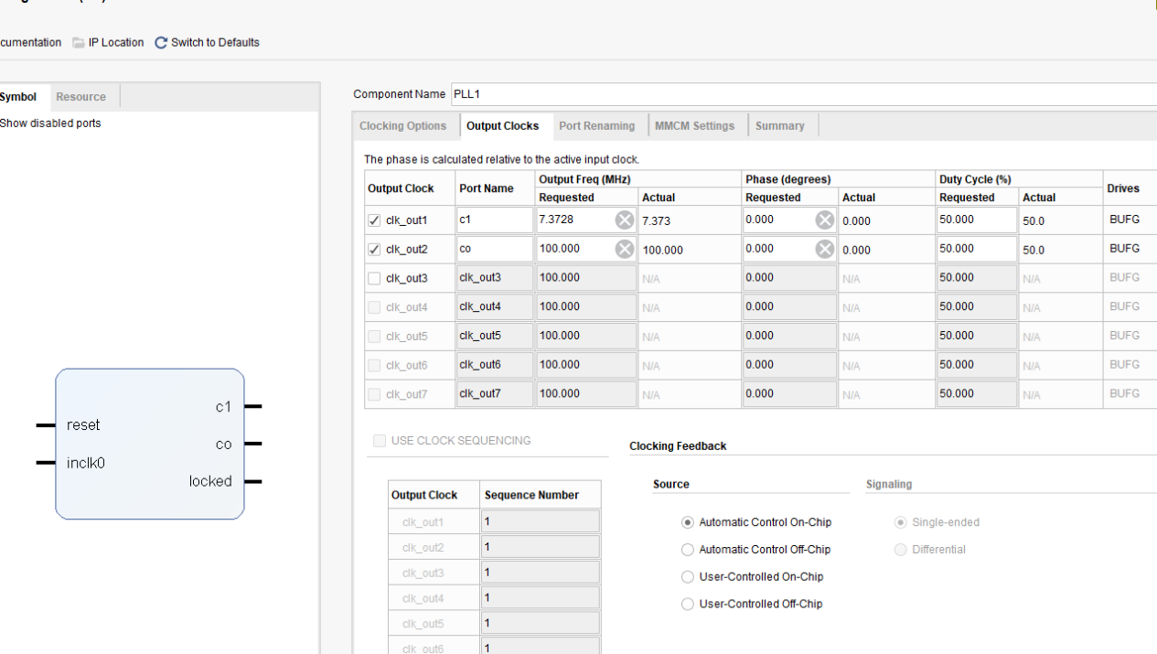
Figure 11.1 PLL setting
- Supported baud rates are 115200,57600,38400,19200
- The default baud rate is 115200
- Design of baud rate
-
-
-
- Instantiate and set it top-level entity
-
-
-
wire tx_band;
wire tx_band;
baud_rate
#(.div(64))
baud_rate_inst
(
.rst (uart_rst),
.inclk (uart_clk),
.baud_sel (baud_sel),
.baud_tx (baud_tx),
);
-
-
-
-
- Baud rate design source file
-
-
-
`timescale 1ns / 10ps
module baud_rate
#(parameter div=64)
(
input rst,
input inclk,
input [1:0] baud_sel,
output reg baud_tx,
output reg baud_rx
);
//Send baud rate, clock frequency division selection
wire [8:0] frq_div_tx;
assign frq_div_tx=(baud_sel==2’b0)?9’d63:
(baud_sel==2’b01)?9’d127:
(baud_sel==2’b10)?9’d255:9’d511;
reg [8:0] count_tx=9’d0;
always@(posedge inclk)
if(rst) begin
count_tx <=9’d0;
baud_tx <=1’b0;
end
else begin
if(count_tx==frq_div_tx) begin
count_tx <=9’d0;
baud_tx<=1’b1;
end
else begin
count_tx<=count_tx+1’b1;
baud_tx<=1’b0;
end
end
//Accept partial baud rate design
wire [6:0] frq_div_rx;
assign frq_div_rx=(baud_sel==2’b0)?7’d7:
(baud_sel==2’b01)?7’d15:
(baud_sel==2’b10)?7’d31:7’d63;
reg [8:0] count_rx=9’d0;
always@(posedge inclk)
if(rst) begin
count_rx <=9’d0;
baud_rx <=1’b0;
end
else begin
if(count_rx==frq_div_rx) begin
count_rx <=9’d0;
baud_rx<=1’b1;
end
else begin
count_rx<=count_rx+1’b1;
baud_rx<=1’b0;
end
end
endmodule
- Design the buffer file tx_buf
- 8-bit FIFO, depth is 256, read/write clock separation, full flag, read empty flag
- Interface and handshake
-
- rst reset signal
- wr_clk write clock
- tx_clk send clock
- 8-bit write data tx_data
- wr_en write enable
- ctrl writes whether the data is a data or a control word
- rdy buffer ready, can accept the next data frame
-
- Send buffer instantiation file
tx_buf
#(.TX_BIT_LEN(8),.STOP_BIT(2))
tx_buf_inst
(
.sys_rst (sys_rst),
.uart_rst (uart_rst),
.wr_clk (sys_clk),
.tx_clk (uart_clk),
.tx_baud (tx_baud),
.tx_wren (tx_wren),
.tx_ctrl (tx_ctrl),
.tx_datain (tx_data),
.tx_done (tx_done),
.txbuf_rdy (txbuf_rdy),
.tx_out (tx_out)
);
- Send buffer source file
`timescale 1ns / 10ps
module tx_buf
#(
parameter TX_BIT_LEN=8,
parameter STOP_BIT=1
)
(
input sys_rst,
input uart_rst,
input wr_clk,
input tx_clk,
input tx_baud,
input tx_wren,
input tx_ctrl,
input tx_done,
input [7:0] tx_datain,
output reg txbuf_rdy,
output tx_out
);
parameter [2:0] TXWR_IDLE=0,
TXWR_RST=1,
TXWR_INIT=2,
TXWR_WAIT=3,
TXWR_WR =4,
TXWR_DONE=5;
parameter [2:0] TXRD_IDLE =0,
TXRD_INIT =1,
TXRD_WAIT0 =2,
TXRD_WAIT1 =3,
TXRD_SEND0 =4,
TXRD_SEND1 =5,
TXRD_DONE =6;
reg wr_clr=1’b1;
reg wr_en;
reg [8:0] wr_data;
reg [5:0]delay;
wire rst_done=(delay==0);
wire trans_rdy;//from low level transmit module
wire wr_full;
reg rd_ack;
wire [8:0] txbuf_q;
reg tx_en;
reg [7:0] tx_len;
wire rd_empty;
reg [7:0] tx_data;
reg [2:0] wr_st,wr_st_nxt;
always@(posedge wr_clk)
if(sys_rst)
wr_st<=TXWR_IDLE;
else
wr_st<=wr_st_nxt;
always@(*) begin
case(wr_st)
TXWR_IDLE: wr_st_nxt=TXWR_RST;
TXWR_RST: begin
if(rst_done)
wr_st_nxt=TXWR_INIT;
else
wr_st_nxt=wr_st;
end
TXWR_INIT: wr_st_nxt=TXWR_WAIT;
TXWR_WAIT:begin
if(!wr_full)
wr_st_nxt=TXWR_WR;
else
wr_st_nxt=wr_st;
end
TXWR_WR: begin
if(tx_done)
wr_st_nxt=TXWR_DONE;
else if(wr_full)
wr_st_nxt=TXWR_WAIT;
else
wr_st_nxt=wr_st;
end
TXWR_DONE: begin
wr_st_nxt=TXWR_INIT;
end
endcase
end
always@(posedge wr_clk) begin
if(wr_st==TXWR_IDLE) begin
wr_clr <=1’b1;
wr_en <=1’b0;
wr_data<=9’b0;
txbuf_rdy <=1’b0;
delay <=31;
end
if(wr_st==TXWR_RST) begin
delay<=delay-1’b1;
end
if(wr_st==TXWR_INIT) begin
wr_clr <=1’b0;
wr_en <=1’b0;
wr_data<=9’b0;
txbuf_rdy <=1’b0;
end
if(wr_st==TXWR_WAIT) begin
wr_clr <=1’b0;
wr_en <=1’b0;
wr_data<=9’b0;
txbuf_rdy <=1’b0;
end
if(wr_st==TXWR_WR) begin
if(tx_done)
txbuf_rdy <=1’b0;
else
txbuf_rdy <=1’b1;
if(tx_wren) begin
wr_en <=1’b1;
wr_data<={tx_ctrl,tx_datain};
end
end
if(wr_st==TXWR_DONE) begin
wr_en <=1’b0;
wr_data<=9’b0;
txbuf_rdy <=1’b0;
end
end
reg [2:0] rd_st,rd_st_nxt;
always@(posedge tx_clk)
if(uart_rst)
rd_st<=TXRD_IDLE;
else
rd_st<=rd_st_nxt;
always@(*)
case(rd_st)
TXRD_IDLE:rd_st_nxt=TXRD_INIT;
TXRD_INIT:begin
if(!rd_empty)
rd_st_nxt=TXRD_WAIT0;
end
TXRD_WAIT0:begin
if(txbuf_q[8])
rd_st_nxt=TXRD_WAIT1;
else if(rd_empty)
rd_st_nxt=TXRD_INIT;
else
rd_st_nxt=rd_st;
end
TXRD_WAIT1:begin
if(trans_rdy)
rd_st_nxt=TXRD_SEND0;
else
rd_st_nxt=rd_st;
end
TXRD_SEND0:begin
rd_st_nxt=TXRD_SEND1;
end
TXRD_SEND1:begin
if(tx_len==0)
rd_st_nxt=TXRD_DONE;
else if(!rd_empty)
rd_st_nxt=TXRD_WAIT1;
else
rd_st_nxt=rd_st;
end
TXRD_DONE:rd_st_nxt=TXRD_INIT;
endcase
always@(posedge tx_clk) begin
case(rd_st)
TXRD_IDLE: begin
rd_ack <=1’b0;
tx_en <=1’b0;
tx_len <=8’b0;
tx_data <=8’b0;
end
TXRD_INIT: begin
rd_ack <=1’b0;
tx_en <=1’b0;
tx_len <=8’b0;
tx_data <=8’b0;
end
TXRD_WAIT0: begin
rd_ack <=1’b1;
tx_en <=1’b0;
tx_len <=txbuf_q[7:0];
tx_data <=txbuf_q[7:0];
end
TXRD_WAIT1: begin
rd_ack <=1’b0;
if(trans_rdy) begin
tx_en <=1’b1;
tx_len <=tx_len -1;
end
else begin
tx_en <=1’b0;
end
end
TXRD_SEND0: begin
rd_ack <=1’b0;
tx_en <=1’b0;
end
TXRD_SEND1: begin
tx_data <=txbuf_q[7:0];
if(trans_rdy)begin
rd_ack <=1’b1;
tx_en <=1’b1;
end
else begin
rd_ack <=1’b0;
tx_en <=1’b0;
end
end
TXRD_DONE: begin
rd_ack <=1’b0;
tx_en <=1’b0;
end
default:;
endcase
end
- Serial transmission, interface and handshake file design
- Interface design
-
-
- tx_rdy, send vacancy, can accept new 8-bit data
- tx_en, send data enable, pass to the sending module 8-bit data enable signal
- tx_data, 8-bit data to be sent
- tx_clk, send clock
- tx_baud, send baud rate
-
-
- Instantiation
tx_transmit
#(.DATA_LEN(TX_BIT_LEN),
.STOP_BIT(STOP_BIT)
)
tx_transmit_inst
(
.tx_rst (uart_rst),
.tx_clk (tx_clk),
.tx_baud (tx_baud),
.tx_en (tx_en),
.tx_data (tx_data),
.tx_rdy (trans_rdy),
.tx_out (tx_out)
);
- Source file
`timescale 1ns / 10ps
module tx_transmit
#(parameter DATA_LEN=8,
parameter STOP_BIT=1
)
(
input tx_rst,
input tx_clk,
input tx_baud,
input tx_en,
input [7:0] tx_data,
output reg tx_rdy,
output reg tx_out
);
parameter [2:0] TX_IDLE=0,
TX_INIT=1,
TX_WAIT=2,
TX_SEND_START=3,
TX_SEND_DATA=4,
TX_SEND_STOP1=5,
TX_SEND_STOP2=6,
TX_DONE=7;
reg [1:0] stop_bit=STOP_BIT;
reg [3:0] tx_len;
reg [8:0] tx_data_r;
reg [2:0] tx_st,tx_st_nxt;
//wire[2:0] tx_len=(stop_bit==0)?7: //8bit
// (stop_bit==1)?6: //7bit
// (stop_bit==2)?5:4; //6bit:5bit
always@(posedge tx_clk)
if(tx_rst)
tx_st<=TX_IDLE;
else
tx_st<=tx_st_nxt;
always@(*)
case(tx_st)
TX_IDLE: tx_st_nxt=TX_INIT;
TX_INIT: tx_st_nxt=TX_WAIT;
TX_WAIT: begin
if(tx_en)
tx_st_nxt=TX_SEND_START;
end
TX_SEND_START: begin
if(tx_baud)
tx_st_nxt=TX_SEND_DATA;
end
TX_SEND_DATA: begin
if((tx_len==0)&tx_baud)
tx_st_nxt=TX_SEND_STOP1;
end
TX_SEND_STOP1: begin
if(tx_baud) begin
if(stop_bit==2’b01)
tx_st_nxt=TX_DONE;
else
tx_st_nxt=TX_SEND_STOP2;
end
end
TX_SEND_STOP2: begin
if(tx_baud)
tx_st_nxt=TX_DONE;
else
tx_st_nxt=tx_st;
end
TX_DONE:begin
tx_st_nxt=TX_IDLE;
end
default:tx_st_nxt=TX_IDLE;
endcase
always@(posedge tx_clk) begin
case(tx_st)
TX_IDLE:begin
tx_rdy <=1’b0;
tx_data_r <=’b0;
tx_len <=3’d0;
tx_out <=1’b1;
end
TX_INIT:begin
tx_rdy <=1’b1;
tx_data_r <=8’b0;
tx_len <=4’d8;
tx_out <=1’b1;
end
TX_WAIT:begin
tx_rdy <=1’b1;
tx_len <=4’d8;
tx_data_r <=tx_data;
tx_out <=1’b1;
end
TX_SEND_START:begin
tx_rdy <=1’b0;
if(tx_baud)
tx_out <=1’b0;
end
TX_SEND_DATA:begin
if(tx_baud) begin
tx_len <=tx_len-1’b1;
tx_out <=tx_data_r[0];
tx_data_r <={1’b0,tx_data_r[7:1]};
end
end
TX_SEND_STOP1:begin
tx_len <=0;
if(tx_baud) begin
tx_out <=1’b1;
end
end
TX_SEND_STOP2:begin
if(tx_baud) begin
tx_out <=1’b1;
end
end
TX_DONE:begin
tx_rdy <=1’b0;
tx_out <=1’b1;
end
default:;
endcase
end
endmodule
- Send testbench.v
`timescale 1ns / 10ps
module tb_uart(
);
reg inclk;
parameter PERIOD = 20;
initial begin
inclk = 1’b0;
//#(PERIOD/2);
end
always
#(PERIOD/2) inclk = ~inclk;
reg rst=0;
wire [1:0] baud_sel=2’b00;
reg tx_wren=0;
reg tx_ctrl=0;
reg [7:0] tx_data=0;
reg [7:0] tx_len=0;
reg tx_done;
wire txbuf_rdy;
wire sys_clk;
wire sys_rst;
reg rx_in=0;
wire tx_out;
initial begin
rst=1’b1;
#100 rst=1’b0;
end
//transmit test
reg [7:0] count=0;
reg [3:0] trans_st;
always@(posedge sys_clk)
if(sys_rst)begin
trans_st <=0;
tx_wren <=1’b0;
tx_ctrl <=1’b0;
tx_data <=8’b0;
tx_done <=1’b0;
tx_len <=0;
tx_len <=0;
count <=8’d0;
end
else case(trans_st)
0:begin
trans_st <=1;
tx_wren <=1’b0;
tx_ctrl <=1’b0;
tx_data <=8’b0;
tx_done <=1’b0;
tx_len <=16;
end
1:begin
tx_wren <=1’b0;
tx_ctrl <=1’b0;
tx_data <=8’b0;
tx_done <=1’b0;
if(txbuf_rdy)
trans_st <=2;
end
2:begin
tx_wren <=1’b1;
tx_ctrl <=1’b1;
tx_data <=tx_len;
trans_st <=3;
end
3:begin
tx_wren <=1’b0;
tx_ctrl <=1’b0;
if(tx_len==0)
trans_st <=4;
else if(txbuf_rdy) begin
tx_data <=count;
count <=count+1;
tx_wren <=1’b1;
tx_len <=tx_len-1;
end
end
4:begin
tx_wren <=1’b0;
tx_ctrl <=1’b0;
tx_data <=0;
tx_len <=16;
tx_done <=1’b1;
trans_st <=5;
end
5:begin
tx_done <=1’b0;
trans_st <=1;
end
endcase
uart_top uart_top_dut
(
.inclk (inclk),
.rst (rst),
.baud_sel (baud_sel),
.tx_wren (tx_wren),
.tx_ctrl (tx_ctrl),
.tx_data (tx_data),
.tx_done (tx_done),
.txbuf_rdy (txbuf_rdy),
.sys_clk (sys_clk),
.sys_rst (sys_rst),
.rx_in (rx_in),
.tx_out (tx_out)
);
endmodule
- Send Modelsim simulation. See Figure 11.2.
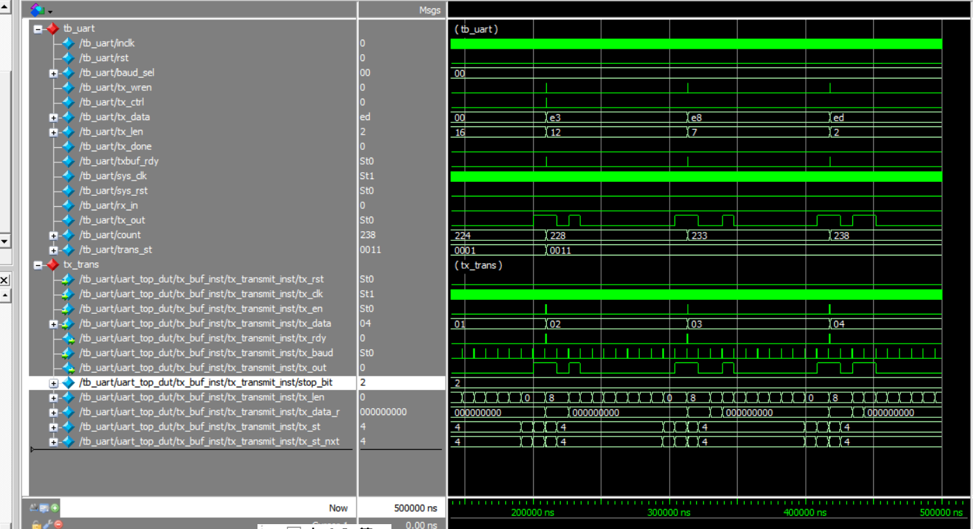
Figure 11.2 ModelSim simulation waves sent by serial
- Extended design (extended content is only reserved for users to think and practice)
- Design the transmitter to support 5, 6, 7, 8-bit PHY (Port physical layer)
- Support parity check
- The settings of the above steps involve FIFO, PLL, etc. (Refer to uart_top project file)
UART accept file design
- Design of rx_phy.v
Design strategies and steps
Use 8 times sampling: so rx_baud is different from tx_baud, here sampling is rx_band = 8*tx_band
Adopting multiple judgments to realize the judgment of receiving data. Determine whether the data counter is greater than 4 after the sampling value is counted.
Steps to receive data:
- Synchronization: refers to how to find the start bit from the received 0101… sync_dtc
- Receive start bit (start)
- Cyclically receive 8-bit data
- Receive stop bit (determine whether it is one stop bit or two stop bits)
Determine if the stop bit is correct
Correct, jump to step 2)
Error, jump to step 1), resynchronize
Do not judge, jump directly 2), this design adopts the scheme of no judgment
- rx_phy source file
module rx_phy
#(
parameter DATA_LEN=8,
parameter STOP_BIT=1
)
(
input rst,
input rx_clk,
input rx_baud,
input rx_in,
output reg [7:0]rx_byte,
output reg rx_rdy
);
localparam [3:0] RX_IDLE=0,
RX_INIT=1,
RX_SYNC=2,
RX_START_DTC=3,
RX_START1=4,
RX_START2=5,
RX_DATA1=6,
RX_DATA2=7,
RX_STOP1=8,
RX_STOP2=9,
RX_DONE=10;
wire [1:0] stop_bit=STOP_BIT;
reg rx_inr=1’b1;
reg [3:0] bit_len=4’d0;
reg [6:0] sync_len=7’b0;
reg [3:0] sample_len=4’d0;
reg [3:0] sample_count=4’d0;
wire bit_value=(sample_count>4);
wire sync_done=(sync_len==0);
reg start_det=1’b0;
reg [3:0] rx_st,rx_st_nxt;
always@(rx_clk)
if(rst)
rx_inr<=1’b1;
else
rx_inr<=rx_in;
always@(posedge rx_clk)
if(rst)
rx_st<=RX_IDLE;
else
rx_st<=rx_st_nxt;
always@(*)
case(rx_st)
RX_IDLE: rx_st_nxt=RX_INIT;
RX_INIT: begin
rx_st_nxt=RX_SYNC;
end
RX_SYNC: begin
if(sync_done)
rx_st_nxt=RX_START_DTC;
else
rx_st_nxt=rx_st;
end
RX_START_DTC:begin
if(start_det)
rx_st_nxt=RX_START1;
else
rx_st_nxt=rx_st;
end
RX_START1:begin
if(sample_len==0)
rx_st_nxt=RX_START2;
else
rx_st_nxt=rx_st;
end
RX_START2:begin
if(sample_count>4)
rx_st_nxt=RX_DATA1;
else
rx_st_nxt=RX_START_DTC;
end
RX_DATA1:begin
if(sample_len==0)
rx_st_nxt=RX_DATA2;
else
rx_st_nxt=rx_st;
end
RX_DATA2:begin
if(bit_len==0)begin
if(stop_bit==2)
rx_st_nxt=RX_STOP1;
else
rx_st_nxt=RX_STOP2;
end
else
rx_st_nxt=RX_DATA1;
end
RX_STOP1:begin
if(rx_baud&(sample_len==0))
rx_st_nxt = RX_STOP2;
end
RX_STOP2:begin
if(rx_baud&(sample_len==0))
rx_st_nxt=RX_DONE;
end
RX_DONE:begin
rx_st_nxt=RX_START_DTC;
end
endcase
always@(posedge rx_clk)
case(rx_st)
RX_IDLE: begin
bit_len <=4’d0;
sync_len<=7’d0;
rx_rdy <=1’b0;
sample_count<=4’d0;
rx_byte <=8’b0;
end
RX_INIT:begin
bit_len <=4’d8;
sync_len <=7’d81;
sample_len <=4’d8;
sample_count<=4’d0;
rx_rdy <=1’b0;
rx_byte <=8’b0;
end
RX_SYNC:begin
if (rx_baud) begin
if(rx_inr)
sync_len<=sync_len-1’b1;
else
sync_len<=7’d81;
end
end
RX_START_DTC:begin
rx_rdy<=1’b0;
sync_len<=7’d81;
rx_byte <=8’b0;
sample_len<=4’d7;
if (rx_baud) begin
if(!rx_inr) begin
start_det<=1’b1;
sample_count<=4’d1;
end
end
end
RX_START1: begin
start_det<=1’b0;
if (rx_baud) begin
if(!rx_inr) begin
sample_count<=sample_count+4’d1;
end
sample_len<=sample_len-1’b1;
end
end
RX_START2:begin
sample_count<=0;
sample_len<=4’d8;
end
RX_DATA1:begin
if (rx_baud) begin
if(rx_inr) begin
sample_count<=sample_count+4’d1;
end
sample_len<=sample_len-1’b1;
end
end
RX_DATA2:begin
sample_len<=4’d8;
sample_count<=0;
bit_len<=bit_len-4’d1;
rx_byte<={bit_value,rx_byte[7:1]};
end
RX_STOP1:begin
bit_len<=4’d7;
if (rx_baud) begin
if(sample_len==0) begin
sample_len<=4’d8;
end
else
sample_len<=sample_len-1’b1;
end
end
RX_STOP2:begin
bit_len<=4’d7;
if (rx_baud) begin
if(sample_len==0) begin
sample_len<=4’d8;
end
else
sample_len<=sample_len-1’b1;
end
end
RX_DONE:begin
rx_rdy<=1’b1;
end
endcase
Endmodule
- The design of rx_buf
Design strategies and steps
- Add 256 depth, 8-bit fifo
-
-
- Read and write clock separation
- Asynchronous clear (internal synchronization)
- Data appears before the rdreq in the read port
-
-
- Steps:
- Initialization: fifo, rx_phy
- Wait: FIFO full signal (wrfull) is 0
- Write: Triggered by rx_phy: rx_phy_byte, rx_phy_rdy
- End of writing
- Back to ii and continue to wait
Rx_buf.v source code
module rx_buf
#(
parameter DATA_LEN=8,
parameter STOP_BIT=1
)
(
input sys_clk,
input rx_clk,
input sys_rst,
input uart_rst,
input rx_in,
input rx_baud,
input rx_rden,
output [7:0] rx_byte,
output reg rx_byte_rdy
);
localparam [2:0] WR_IDLE=0,
WR_RST =1,
WR_INIT=2,
WR_WAIT=3,
WR_WR =4,
WR_DONE=5;
wire wr_full;
wire rd_empty;
wire wr_rst_busy;
reg wr_clr=0;
reg wr_en=0;
reg [7:0] wr_data=0;
wire [7:0] rx_phy_byte;
wire rx_phy_rdy;
//wire rd_rst_busy;
reg [2:0] wr_st,wr_st_nxt;
always@(posedge sys_clk)
if(sys_rst)
rx_byte_rdy<=1’b0;
else
rx_byte_rdy<=!rd_empty;
always@(posedge rx_clk)
if(uart_rst)
wr_st<= WR_IDLE;
else
wr_st<=wr_st_nxt;
always@(*)
case(wr_st)
WR_IDLE: wr_st_nxt=WR_RST;
WR_RST : begin
// if(wr_rst_busy)
// wr_st_nxt=wr_st;
// else
wr_st_nxt=WR_INIT;
end
WR_INIT: begin
wr_st_nxt=WR_WAIT;
end
WR_WAIT: begin
if(!wr_full)
wr_st_nxt=WR_WR;
end
WR_WR: begin
if(rx_phy_rdy)
wr_st_nxt=WR_DONE;
end
WR_DONE: begin
wr_st_nxt=WR_WAIT;
end
endcase
always@(posedge rx_clk)
case(wr_st)
WR_IDLE:begin
wr_clr <=1’b1;
wr_en <=1’b0;
wr_data <=8’d0;
end
WR_RST: begin
wr_clr <=1’b0;
wr_en <=1’b0;
wr_data <=8’d0;
end
WR_INIT: begin
wr_clr <=1’b0;
wr_en <=1’b0;
wr_data <=8’d0;
end
WR_WAIT: begin
wr_clr <=1’b0;
wr_en <=1’b0;
wr_data <=8’d0;
end
WR_WR:begin
wr_en <=rx_phy_rdy;
wr_data <=rx_phy_byte;
end
WR_DONE: begin
wr_en <=1’b0;
wr_data <=8’d0;
end
endcase
rx_phy
#(
.DATA_LEN(8),
.STOP_BIT(1)
)
rx_phy_inst
(
.rst (uart_rst),
.rx_clk (rx_clk),
.rx_baud (rx_baud),
.rx_in (rx_in),
.rx_byte (rx_phy_byte),
.rx_rdy (rx_phy_rdy)
);
rx_fifo rx_fifo_inst
(
.aclr (wr_clr),
.data (wr_data),
.rdclk (sys_clk),
.rdreq (rx_rden),
.wrclk (rx_clk),
.wrreq (wr_en),
.q (rx_byte),
.rdempty (rd_empty),
.wrfull (wr_full)
//.wr_rst_busy (wr_rst_busy),
// .rd_rst_busy (rd_rst_busy)
);
Endmodule
-
- Receive simulation incentive
Content and steps
-
-
- tx, rx loopback test (assign rx_in = tx_out)
- Continue to use the incentive file in the TX section
- Writing the incentive part of rx
-
Some parts of tb_uart.v
assign rx_in=tx_out;
wire [7:0] rx_byte;
wire rx_byte_rdy;
reg [7:0] rx_byte_r;
reg rx_rden;
always@(posedge sys_clk)
if(rx_byte_rdy)begin
rx_rden <=1’b1;
rx_byte_r<=rx_byte;
end
else begin
rx_rden<=1’b0;
end
uart_top uart_top_dut
(
.inclk (inclk),
.rst (rst),
.baud_sel (baud_sel),
.tx_wren (tx_wren),
.tx_ctrl (tx_ctrl),
.tx_data (tx_data),
.tx_done (tx_done),
.txbuf_rdy (txbuf_rdy),
.rx_rden (rx_rden),
.rx_byte (rx_byte),
.rx_byte_rdy(rx_byte_rdy),
.sys_clk (sys_clk),
.sys_rst (sys_rst),
.rx_in (rx_in),
.tx_out (tx_out)
);
-
- ModelSim simulation. See Figure 11.3.
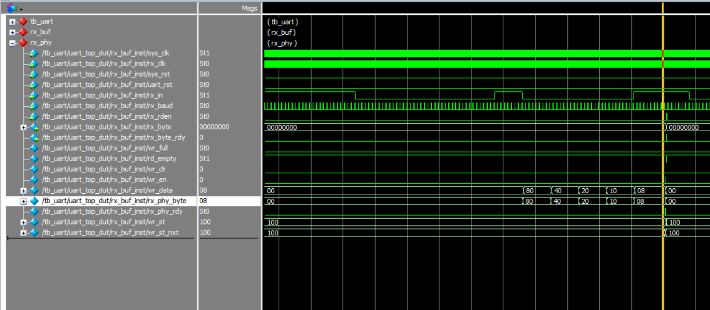
Figure 11.3 Simulation
Reflection and expansion
- Modify the program to complete the 5, 6, 7, 8-bit design
- Completing the design of the resynchronization when the start and stop have errors of the receiving end rx_phy
- Complete the analysis and packaging of the receipt frame of rx_buf
- Using multi-sampling to design 180° alignment of data, compare with FPGA resources, timing and data recovery effects
Hardware test
-
-
- Use develop board to test
-
USB_B
J3
USB to UART
TXD
RXD
Figure 11.4 USB to serial conversion
Write a hardware test file.
-
-
- Development board J3 is connected to the host USB interface
- Using test software such as teraterm, SSCOM3, etc. You can also write a serial communication program (C#, C++, JAVA, Python…).
- PC sends data in a certain format
- The test end uses a counter to generate data in a certain format.
- Development board J3 is connected to the host USB interface
-
The test procedure is as follows module hw_tb_uart
(
input inclk,
input rst,
input [1:0] baud_sel,
input rx_in,
output tx_out
);
reg tx_wren=0;
reg tx_ctrl=0;
reg [7:0] tx_data=0;
reg [7:0] tx_len=0;
reg tx_done;
wire txbuf_rdy;
wire sys_clk;
wire sys_rst;
//transmit test
reg [7:0] count=0;
reg [3:0] trans_st;
always@(posedge sys_clk)
if(sys_rst)begin
trans_st <=0;
tx_wren <=1’b0;
tx_ctrl <=1’b0;
tx_data <=8’b0;
tx_done <=1’b0;
tx_len <=0;
tx_len <=0;
count <=8’d0;
end
else case(trans_st)
0:begin
trans_st <=1;
tx_wren <=1’b0;
tx_ctrl <=1’b0;
tx_data <=8’b0;
tx_done <=1’b0;
tx_len <=16;
end
1:begin
tx_wren <=1’b0;
tx_ctrl <=1’b0;
tx_data <=8’b0;
tx_done <=1’b0;
if(txbuf_rdy)
trans_st <=2;
end
2:begin
tx_wren <=1’b1;
tx_ctrl <=1’b1;
tx_data <=tx_len;
trans_st <=3;
end
3:begin
tx_wren <=1’b0;
tx_ctrl <=1’b0;
if(tx_len==0)
trans_st <=4;
else if(txbuf_rdy) begin
tx_data <=count;
count <=count+1;
tx_wren <=1’b1;
tx_len <=tx_len-1;
end
end
4:begin
tx_wren <=1’b0;
tx_ctrl <=1’b0;
tx_data <=0;
tx_len <=16;
tx_done <=1’b1;
trans_st <=5;
end
5:begin
tx_done <=1’b0;
trans_st <=1;
end
endcase
wire [7:0] rx_byte;
wire rx_byte_rdy;
reg [7:0] rx_byte_r;
reg rx_rden;
always@(posedge sys_clk)
if(rx_byte_rdy)begin
rx_rden <=1’b1;
rx_byte_r<=rx_byte;
end
else begin
rx_rden<=1’b0;
end
uart_top uart_top_dut
(
.inclk (inclk),
.rst (rst),
.baud_sel (baud_sel),
.tx_wren (tx_wren),
.tx_ctrl (tx_ctrl),
.tx_data (tx_data),
.tx_done (tx_done),
.txbuf_rdy (txbuf_rdy),
.rx_rden (rx_rden),
.rx_byte (rx_byte),
.rx_byte_rdy(rx_byte_rdy),
.sys_clk (sys_clk),
.sys_rst (sys_rst),
.rx_in (rx_in),
.tx_out (tx_out)
);
endmodule
- Lock the pins, and test
| Signal Name | Port Description | Network Label | FPGA Pin |
| clk | System clock, 50 MHz | C10_50MCLK | U22 |
| rst_n | Reset, high by default | KEY1 | M4 |
| tx_data[0] | Switch input | GPIO_DIP_SW0 | N8 |
| tx_data[1] | Switch input | GPIO_DIP_SW1 | M5 |
| tx_data[2] | Switch input | GPIO_DIP_SW2 | P4 |
| tx_data[3] | Switch input | GPIO_DIP_SW3 | N4 |
| tx_data[4] | Switch input | GPIO_DIP_SW4 | U6 |
| tx_data[5] | Switch input | GPIO_DIP_SW5 | U5 |
| tx_data[6] | Switch input | GPIO_DIP_SW6 | R8 |
| tx_data[7] | Switch input | GPIO_DIP_SW7 | P8 |
| tx_out | Serial output | TTL_RX | L18 |
| rx_in | Serial input | TTL_TX | L17 |
| txbuf_rdy | Segment a | SEG_PA | P24 |
| rx_byte_rdy | Segment h | SEG_DP | K26 |
| weixuan | Segment 1 | SEG_3V3_D0 | R16 |
| rx_byte[0] | LED 0 | LED0 | N17 |
| rx_byte[1] | LED 1 | LED1 | M19 |
| rx_byte[2] | LED 2 | LED2 | P16 |
| rx_byte[3] | LED 3 | LED3 | N16 |
| rx_byte[4] | LED 4 | LED4 | N19 |
| rx_byte[5] | LED 5 | LED5 | P19 |
| rx_byte[6] | LED 6 | LED6 | N24 |
| rx_byte[7] | LED 7 | LED7 | N23 |
| tx_wren | Write control | KEY2 | L4 |
| tx_ctrl | Write data control | KEY3 | L5 |
| tx_done | Write ending control | KEY4 | K5 |
| rx_rden | Read enable | KEY5 | R1 |
- Observe the data received
- Using ILA to observe the data sent by FPGA
- See Figure 11.5, when FPGA sends A0
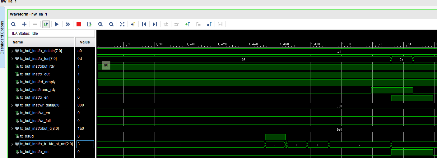
Figure 11.5 Sending A0
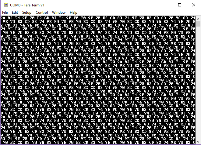
Figure 11.6 Data receive by host computer
- The receiving part has been eliminated here. You are encouraged to try it on your own.
Experiment 12 IIC Protocol Transmission
1.Experiment Objective
There is an IIC interface EEPROM chip 24LC02 in the test plate, capacity sized 2 kbit (256 bite). Since the data is not lost after the EEPROM is powered down, users can store some hardware setup data or user information.
Learning the basic principles of the different IIC bus, mastering the IIC communication protocol
Master the method of reading and writing EEPROM
Joint debugging using logic analyzer
2.Experiment Implement
Correctly write a number to any address in the EEPROM (this experiment writes to the register of 8’h03 address) through the FPGA (here changes the written 8-bit data value by (SW7~SW0)). After writing in successfully, read the data as well. The read data is displayed directly on the segment decoders.
Download the program into the FPGA and press the Up button PB2 to execute the data write EEPROM operation. Press the Return button PB3 to read the data that was just written.
-
- Determine whether the value read is correct or not by reading the value displayed on the segment decoders. If the segment decoders display the same value as written value, the experiment is successful.
Analyze the correctness of the internal data with ILA and verify it with the display of the segment decoders.
3.Introduction to the IIC Agreement
3.1 The Overall Timing Protocol of IIC Is as Follows
Bus idle state: SDA, SCL are high
Start of IIC protocol: SCL stays high, SDA jumps from high level to low level, generating a start signal
IIC read and write data phase: including serial input and output of data and response model issued by data receiver
IIC transmission end bit: SCL is high level, SDA jumps from low level to high level, and generates an end flag. See Figure 12.1.
Figure 12.1 Timing protocol of IIC
3.2 IIC Device Address
Each IIC device has a device address. When some device addresses are shipped from the factory, they are fixed by the manufacturer (the specific data can be found in the manufacturer’s data sheet). Some of their higher bits are determined, and the lower bits can be configured by the user according to the requirement. The higher four-bit address of the EEPROM chip 24LC02 used by the develop board has been fixed to 1010 by the component manufacturer. The lower three bits are linked in the develop board as shown below, so the device address is 1010000. (The asterisk resistance indicates that it is not soldered). See Figure 12.2.
Figure 12.2 IIC device schematics
4. Main Code
|
5.Downloading to The Board
Lock the Pins
| Signal Name | Port Description | Network Label | FPGA Pin |
| clk | System clock, 50 MHz | C10_50MCLK | U22 |
| rst_n | Reset, high by default | KEY1 | M4 |
| sm_db[0] | Segment a | SEG_PA | K26 |
| sm_db [1] | Segment b | SEG_PB | M20 |
| sm_db [2] | Segment c | SEG_PC | L20 |
| sm_db [3] | Segment d | SEG_PD | N21 |
| sm_db [4] | Segment e | SEG_PE | N22 |
| sm_db [5] | Segment f | SEG_PF | P21 |
| sm_db [6] | Segment g | SEG_PG | P23 |
| sm_db [7] | Segment h | SEG_DP | P24 |
| sm_cs1_n | Segment 2 | SEG_3V3_D0 | R16 |
| sm_cs2_n | Segment 1 | SEG_3V3_D1 | R17 |
| data[0] | Switch input | GPIO_DIP_SW0 | N8 |
| data[1] | Switch input | GPIO_DIP_SW1 | M5 |
| data[2] | Switch input | GPIO_DIP_SW2 | P4 |
| data[3] | Switch input | GPIO_DIP_SW3 | N4 |
| data[4] | Switch input | GPIO_DIP_SW4 | U6 |
| data[5] | Switch input | GPIO_DIP_SW5 | U5 |
| data[6] | Switch input | GPIO_DIP_SW6 | R8 |
| data[7] | Switch input | GPIO_DIP_SW7 | P8 |
| sw1 | Write EEPROM | KEY2 | L4 |
| sw2 | Read EEPROM | KEY3 | L5 |
| scl | EEPROM clock | I2C_SCl | R20 |
| sda | EEPROM data line | I2C_SDA | R21 |
After the program is downloaded to the board, press the Up push button PB2 to write the 8-bit value represented by SW7~SW0 to EEPROM. Then press the Return button PB3 to read the value from the written position. Observe the value displayed on the segment decoders on the develop board and the value written in the 8’h03 register of the EEPROM address (SW7~SW0) (Here, it writes to 8’h37 address). The read value is displayed on the segment decoders. See Figure 12.3.
Figure 12.3 Demonstration of the develop board
Figure 12.4 ILA demonstration
6.More to Practice
Try to write to eeprom multiple non-contiguous addresses and read them. Prepare for the next experiment.
Experiment 13 AD, DA Experiment
1.Experiment Objective
Since in the real world, all naturally occurring signals are analog signals, and all that are read and processed in actual engineering are digital signals. There is a process of mutual conversion between natural and industrial signals (digital-to-analog conversion: DAC, analog-to-digital conversion: ADC). The purpose of this experiment is twofold:
- Learning the theory of AD conversion
- Read the value of AD acquisition from PCF8591, and convert the value obtained into actual value, display it with segment decoders
2.Experiment Implement
Perform analog-to-digital conversion using the ADC port of the chip and display the collected voltage value through the segment decoders.
Board downloading verification for comparison
Introduction to PCF8591: The PCF8591 uses the IIC bus protocol to communicate with the controller (FPGA). Please refer to the previous experiment for the contents of the IIC bus protocol. The first four bits of the device address are 1001, and the last three bits are determined by the actual circuit connection (here the circuit is grounded, so the device address is 7’b1001000). The LSB is the read/write control signal. After sending the device address information and the read/write control word are done, the control word information is sent. The specific control word information is shown in Figure 13.1.
Figure 13.1 PCF8591 Control address
Here, the experiment uses the DIP switch (SW1, SW0) input channel as the AD acquisition input channel. Configure the control information as (8’h40). For more details, refer to the datasheet of PCF8591.
| SW1,SW0 | Channel Selection | Collection Object |
| 00 | 0 | Photosensitive Resistor Voltage Value |
| 01 | 1 | Thermistor Voltage Value |
| 10 | 2 | Adjustable Voltage Value |
3.Experiment Design
- Program design and review the top-down design method used before.
- The top-level entity is divided into three parts: the segment decoder driver part, the AD sampling part of the PCF and the IIC serial port driver part.
IIC serial driver part code is as follows:
|
Segment decoder driver part is as follow:
| module led_seg7(
clk,rst_n, dis_data, point1 , sel,sm_db ); input clk; input rst_n; input[7:0] dis_data; output reg [5:0] sel; output[6:0] sm_db; output reg point1 ; reg[11:0] cnt1; reg[2:0] cnt; reg [3:0] num; wire en=(cnt1==12’hfff) ?1:0 ; parameter V_REF = 12’d3300 ; reg [19:0] num_t ; reg [19:0] num1 ; always @ (posedge clk) num_t <= V_REF *dis_data ; wire [3:0] data0 ; wire [3:0] data1 ; wire [3:0] data2 ; wire [3:0] data3 ; wire [3:0] data4 ; wire [3:0] data5 ; assign data5 = num1 / 17’d100000; assign data4 = num1 / 14’d10000 % 4’d10; assign data3 = num1 / 10’d1000 % 4’d10 ; assign data2 = num1 / 7’d100 % 4’d10 ; assign data1 = num1 / 4’d10 % 4’d10 ; assign data0 = num1 % 4’d10; always @(posedge clk or negedge rst_n) begin if(rst_n == 1’b0) begin num1 <= 20’d0; end else num1 <= num_t >> 4’d8; end always @ (posedge clk or negedge rst_n) if(!rst_n) cnt1 <= 4’d0; else cnt1 <= cnt1+1’b1; parameter seg0 = 7’h3f, seg1 = 7’h06, seg2 = 7’h5b, seg3 = 7’h4f, seg4 = 7’h66, seg5 = 7’h6d, seg6 = 7’h7d, seg7 = 7’h07, seg8 = 7’h7f, seg9 = 7’h6f, sega = 7’h77, segb = 7’h7c, segc = 7’h39, segd = 7’h5e, sege = 7’h79, segf = 7’h71; reg[6:0] sm_dbr; always @ (*) case (num) 4’h0: sm_dbr = seg0; 4’h1: sm_dbr = seg1; 4’h2: sm_dbr = seg2; 4’h3: sm_dbr = seg3; 4’h4: sm_dbr = seg4; 4’h5: sm_dbr = seg5; 4’h6: sm_dbr = seg6; 4’h7: sm_dbr = seg7; 4’h8: sm_dbr = seg8; 4’h9: sm_dbr = seg9; 4’ha: sm_dbr = sega; 4’hb: sm_dbr = segb; 4’hc: sm_dbr = segc; 4’hd: sm_dbr = segd; 4’he: sm_dbr = sege; 4’hf: sm_dbr = segf; default: ; endcase assign sm_db = sm_dbr; always @ (posedge clk or negedge rst_n) begin if(!rst_n) begin sel <= 6’b000000; num <= 4’b0; cnt<=3’b000; end else begin case (cnt) 3’d0 :begin sel <= 6’b111111; num <= data5 ; point1 <= 1’b1 ; if(en) cnt<=3’d1 ; end 3’d1 :begin sel <= 6’b111111; num <= data4 ; point1 <=1’b1 ; if(en) cnt<=3’d2 ; end 3’d2 :begin sel <= 6’b111011; num <= data3; point1 <= 1’b0 ; if(en) cnt<=3’d3 ; end 3’d3 :begin sel <= 6’b110111; num <= data2; point1 <= 1’b1 ; if(en) cnt<=3’d4 ; end 3’d4 :begin sel <= 6’b101111; num <= data1; point1 <=1’b1; if(en) cnt<=3’d5 ; end 3’d5 :begin sel <= 6’b011111; num <= data0; point1 <=1’b1; if(en) cnt<=3’d0 ; end default :begin sel <= 6’b000000; num <= 4’h0; point1 <= 1’b1; end endcase end end endmodule |
4.Downloading to The Board
-
-
- Lock the pins
-
| SignaL Name | Port Description | Network Label | FPGA Pin |
| clk | System clock, 50 MHz | C10_50MCLK | U22 |
| rst_n | Reset, high by default | KEY1 | M4 |
| sm_db[0] | Segment a | SEG_PA | K26 |
| sm_db [1] | Segment b | SEG_PB | M20 |
| sm_db [2] | Segment c | SEG_PC | L20 |
| sm_db [3] | Segment d | SEG_PD | N21 |
| sm_db [4] | Segment e | SEG_PE | N22 |
| sm_db [5] | Segment f | SEG_PF | P21 |
| sm_db [6] | Segment g | SEG_PG | P23 |
| sm_db [7] | Segment h | SEG_DP | P24 |
| data[0] | Switch input | GPIO_DIP_SW0 | N8 |
| data[1] | Switch input | GPIO_DIP_SW1 | M5 |
| data[2] | Switch input | GPIO_DIP_SW2 | P4 |
| data[3] | Switch input | GPIO_DIP_SW3 | N4 |
| data[4] | Switch input | GPIO_DIP_SW4 | U6 |
| data[5] | Switch input | GPIO_DIP_SW5 | U5 |
| data[6] | Switch input | GPIO_DIP_SW6 | R8 |
| data[7] | Switch input | GPIO_DIP_SW7 | P8 |
| scl | PCF8591 clock | ADDA_I2C_SCl | E20 |
| sda | PCF8591 data line | ADDA_I2C_SDA | C19 |
| sel[0] | Segment decoder position selection | SEG_3V3_D0 | R16 |
| sel[1] | Segment decoder position selection | SEG_3V3_D1 | R17 |
| sel[2] | Segment decoder position selection | SEG_3V3_D2 | N18 |
| sel[3] | Segment decoder position selection | SEG_3V3_D3 | K25 |
| sel[4] | Segment decoder position selection | SEG_3V3_D4 | R25 |
| sel[5] | Segment decoder position selection | SEG_3V3_D5 | T24 |
-
-
- Testing by selecting SW0 and SW1 to change the measurement objects.
-
Figure 13.2 Test result
Experiment 14 HDMI Graphic Display Experiment
1.Experiment Objective
- Learn about video timing
(2) Understand the register configuration of the ADV7511, reviewing the knowledge from experiment 12
2.Experiment Implement
- Image display processing has always been the focus of FPGA research. At present, the image display mode is also developing. The image display interface is also gradually transitioning from the old VGA interface to the new DVI or HDMI interface.
- Display the image using the HDMI interface of the development board.
- Download the program to the board for comparison.
- Introduction to HDMI: HDMI (High Definition Multimedia Interface) is a digital video/audio interface technology. It is a dedicated digital interface for image transmission. It can transmit audio and video signals at the same time.
- Introduction to ADV7511: The ADV7511 is a chip that converts FPGA digital signal to HDMI signal following VESA standard. For more details, see the related chip manual. Among them, “ADV7511 Programming Guide” and “ADV7511 Hardware Users Guide” are the most important. From Table 16 on page 27 of “ADV7511 Programming Guide”, the bit width and format type of RGB can be configured. Its registers can output the appropriate format according to needs after configuration.
- ADV7511 Register Configuration Description: The bus inputs D0-D3, D12-D15, and D24-D27 of the ADV7511 have no input, that is, RGB4:4:4, and each bit of data is in 8-bit mode. Directly set 0x15 [3:0] to 0x0. Set [5:4] of 0X16 to 11 and keep the default values for the other digits. 0x17[1] refers to the ratio of the length to the width of the image. It can be set to 0 or 1. The actual LCD screen will not change according to the data, but will automatically stretch the full screen mode according to the LCD’s own settings. 0x18[7] is the way to start the color range stretching. The design is that RGB maps directly to RGB, so it can be disabled directly. 0XAF[1] is the setting of choosing either HDMI or DVI mode. The most direct point of HDMI over DVI is that HDMI can send digital audio data and encrypt data content. This experiment only needs to display the picture, and it can be set directly to DVI mode. 0XAF[7], set to 0 to turn off HDMI encryption. Due to GCCD, deep color encryption data is not applicable, so the GC option is turned off. 0xAF[7] is set to 0 to turn off the GC CD data.
Timing and Data Generation
(1280 x 720 @ 60 Hz)
ADV7511
Crystal Osciilation
Figure 14.1 HDMI connection block diagram
3.Program Design
3.1 Schematics
Figure 14.2 Schematics of ADV7511
3.2 Main Code
-
- 1080p VGA main part of the timing generation program
|
-
- Main part of register configuration
Directly use the above experimental content for IIC interface configuration register. Here is mainly about the register configuration part
| case( i )
0: if( iic_done ) begin isStart <= 2’b00; i <= i + 1’b1; end else begin isStart <= 2’b01; rData <= 8’h50; rAddr <= 8’h41; end 1: if( iic_done ) begin isStart <= 2’b00; i <= i + 1’b1; end else begin isStart <= 2’b01; rData <= 8’h10; rAddr <= 8’h41; end 2: if( iic_done ) begin isStart <= 2’b00; i <= i + 1’b1; end else begin isStart <= 2’b01; rData <= 8’h03; rAddr <= 8’h98; end 3: if( iic_done ) begin isStart <= 2’b00; i <= i + 1’b1; end else begin isStart <= 2’b01; rData <= 8’h03; rAddr <= 8’h9a; end 4: if( iic_done ) begin isStart <= 2’b00; i <= i + 1’b1; end else begin isStart <= 2’b01; rData <= 8’h30; rAddr <= 8’h9c; end 5: if( iic_done ) begin isStart <= 2’b00; i <= i + 1’b1; end else begin isStart <= 2’b01; rData <= 8’h01; rAddr <= 8’h9d; end 6: if( iic_done ) begin isStart <= 2’b00; i <= i + 1’b1; end else begin isStart <= 2’b01; rData <= 8’ha4; rAddr <= 8’ha2; end 7: if( iic_done ) begin isStart <= 2’b00; i <= i + 1’b1; end else begin isStart <= 2’b01; rData <= 8’ha4; rAddr <= 8’ha3; end 8: if( iic_done ) begin isStart <= 2’b00; i <= i + 1’b1; end else begin isStart <= 2’b01; rData <= 8’hd0; rAddr <= 8’he0; end 9: if( iic_done ) begin isStart <= 2’b00; i <= i + 1’b1; end else begin isStart <= 2’b01; rData <= 8’h00; rAddr <= 8’hf9; end 10: if( iic_done ) begin isStart <= 2’b00; i <= i + 1’b1; end else begin isStart <= 2’b01; rData <= 8’h20; rAddr <= 8’h15; end 11: if( iic_done ) begin isStart <= 2’b00; i <= i + 1’b1; end else begin isStart <= 2’b01; rData <= 8’h30; rAddr <= 8’h16; end 12: if( iic_done ) begin isStart <= 2’b00; i <= i + 1’b1; end else begin isStart <= 2’b01; rAddr <= 8’haf; rData <= 8’h02;end 13: if( iic_done ) begin isStart <= 2’b00; i <= i + 1’b1; end else begin isStart <= 2’b01; rAddr <= 8’h01; rData <= 8’h00;end 14: if( iic_done ) begin isStart <= 2’b00; i <= i + 1’b1; end else begin isStart <= 2’b01; rAddr <= 8’h02; rData <= 8’h18;end 15: if( iic_done ) begin isStart <= 2’b00; i <= i + 1’b1; end else begin isStart <= 2’b01; rAddr <= 8’h03; rData <= 8’h00;end 16: if( iic_done ) begin isStart <= 2’b00; i <= i + 1’b1; end else begin isStart <= 2’b01; rAddr <= 8’h0a; rData <= 8’h03;end 17: if( iic_done ) begin isStart <= 2’b00; i <= i + 1’b1; end else begin isStart <= 2’b01; rAddr <= 8’h0b; rData <= 8’h6e;end 18: if( iic_done ) begin isStart <= 2’b00; i <= i + 1’b1; end else begin isStart <= 2’b01; rAddr <= 8’h0c; rData <= 8’hbd;end 19: if( iic_done ) begin isStart <= 2’b00; i <= i + 1’b1; end else begin isStart <= 2’b01; rAddr <= 8’hd6; rData <= 8’hc0;end endcase |
Board Verification
- Lock the pins
| Signal Name | Port Description | Network Label | FPGA Pin |
| clk_in | System clock, 50 MHz | C10_50MCLK | U22 |
| rst_n | Reset, high by default | KEY1 | M4 |
| vga_hs | Horizontal synchronous signal | HDMI_HSYNC | C24 |
| vga_vs | Vertical synchronous signal | HDMI_VSYNC | A25 |
| en | Date valid | HDMI_DE | A24 |
| vga_clk | Display clock | HDMI_CLK | B19 |
| key1 | Display effect toggle button | KEY2 | L4 |
| scl | ADV7511 configuration clock | I2C_SCL | R20 |
| sda | ADV7511 configuration data | I2C_SDA | R21 |
| vag_r[7] | Red output | HDMI_D23 | F15 |
| vag_r[6] | Red output | HDMI_D22 | E16 |
| vag_r[5] | Red output | HDMI_D21 | D16 |
| vag_r[4] | Red output | HDMI_D20 | G17 |
| vag_r[3] | Red output | HDMI_D19 | E17 |
| vag_r[2] | Red output | HDMI_D18 | F17 |
| vag_r[1] | Red output | HDMI_D17 | C17 |
| vag_r[0] | Red output | HDMI_D16 | A17 |
| vag_g[7] | Green output | HDMI_D15 | B17 |
| vag_g[6] | Green output | HDMI_D14 | C18 |
| vag_g[5] | Green output | HDMI_D13 | A18 |
| vag_g[4] | Green output | HDMI_D12 | D19 |
| vag_g[3] | Green output | HDMI_D11 | D20 |
| vag_g[2] | Green output | HDMI_D10 | A19 |
| vag_g[1] | Green output | HDMI_D9 | B20 |
| vag_g[0] | Green output | HDMI_D8 | A20 |
| vag_b[7] | Blue output | HDMI_D7 | B21 |
| vag_b[6] | Blue output | HDMI_D6 | C21 |
| vag_b[5] | Blue output | HDMI_D5 | A22 |
| vag_b[4] | Blue output | HDMI_D4 | B22 |
| vag_b[3] | Blue output | HDMI_D3 | C22 |
| vag_b[2] | Blue output | HDMI_D2 | A23 |
| vag_b[1] | Blue output | HDMI_D1 | D21 |
| vag_b[0] | Blue output | HDMI_D0 | B24 |
- Comprehensive compilation and downloading the program to the board. Each time you press the UP button on the development board, you can see the different display effects on the computer monitor to switch. The effect is as follows:
Figure 14. 3 HDMI display
Experiment 15 Ethernet
15.1 Experiment Objective
- Understand what Ethernet is and how it works
- Familiar with the relationship between different interface types (MII, GMII, RGMII) and their advantages and disadvantages (FII-PRA040 uses RGMII)
- Combine the development board to complete the transmission and reception of data and verify it
15.2 Experiment Implement
- Perform a loopback test to check if the hardware is working properly.
- Perform data receiving verification
- Perform data transmission verification
15.3 Experiment
15.3.1 Introduction to Experiment Principle
Ethernet is a baseband LAN technology. Ethernet communication is a communication method that uses coaxial cable as a network media and uses carrier multi-access and collision detection mechanisms. The data transmission rate reaches 1 Gbit/s, which can satisfy the need for data transfer of non-persistent networks. As an interconnected interface, the Ethernet interface is very widely used. There are many types of Gigabit Ethernet MII interfaces, GMII and RGMII are commonly used.
MII interface has a total of 16 lines. See Figure 15.1.
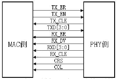
PHY SIDE
MAC SIDE
Figure 15.1 MII interface
RXD(Receive Data)[3:0]: data reception signal, a total of 4 signal lines;
TX_ER(Transmit Error): Send data error prompt signal, synchronized to TX_CLK, active high, indicating that the data transmitted during TX_ER validity period is invalid. For 10Mbps rate, TX_ER does not work;
RX_ER(Receive Error): Receive data error prompt signal, synchronized to RX_CLK, active high, indicating that the data transmitted during the valid period of RX_ER is invalid. For 10 Mbps speed, RX_ER does not work;
TX_EN(Transmit Enable): Send enable signal, only the data transmitted during the valid period of TX_EN is valid;
RX_DV(Reveive Data Valid): Receive data valid signal, the action type is TX_EN of the transmission channel;
TX_CLK: Transmit reference clock, the clock frequency is 25 MHz at 100 Mbps, and the clock frequency is 2.5 MHz at 10 Mbps. Note that the direction of TX_CLK clock is from the PHY side to the MAC side, so this clock is provided by the PHY;
RX_CLK: Receive data reference clock, the clock frequency is 25 MHz at 100 Mbps, and the clock frequency is 2.5 MHz at 10 Mbps. RX_CLK is also provided by the PHY side;
CRS: Carrier Sense, carrier detect signal, does not need to synchronize with the reference clock. As long as there is data transmission, CRS is valid. In addition, CRS is effective only if PHY is in half-duplex mode;
COL: Collision detection signal, does not need to be synchronized to the reference clock, is valid only if PHY is in half-duplex mode.
GMII interface is shown in Figure 15. 2.
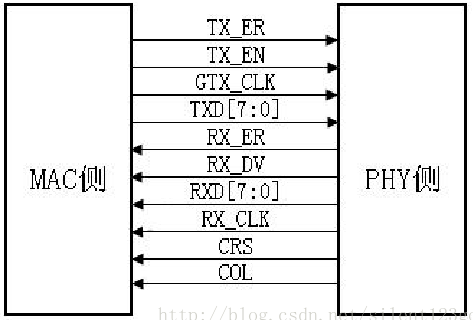
PHY SIDE
MAC SIDE
Figure 15.2 GMII interface
Compared with the MII interface, the data width of the GMII is changed from 4 bits to 8 bits. The control signals in the GMII interface such as TX_ER, TX_EN, RX_ER, RX_DV, CRS, and COL function the same as those in the MII interface. The frequencies of transmitting reference clock GTX_CLK and the receiving reference clock RX_CLK are both 125 MHz (1000 Mbps / 8 = 125 MHz).
There is one point that needs special explanation here, that is, the transmitting reference clock GTX_CLK is different from the TX_CLK in the MII interface. The TX_CLK in the MII interface is provided by the PHY chip to the MAC chip, and the GTX_CLK in the GMII interface is provided to the PHY chip by the MAC chip. The directions are different.
See Figure 15.3 for RGMII interface.
In practical applications, most GMII interfaces are compatible with MII interfaces. Therefore, the general GMII interface has two transmitting reference clocks: TX_CLK and GTX_CLK (the directions of the two are different, as mentioned above). When used as the MII mode, TX_CLK and 4 of the 8 data lines are used.
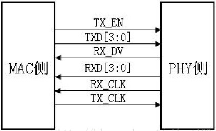
PHY SIDE
MAC SIDE
Figure 15.3 RGMII interface
RGMII, or reduced GMII, is a simplified version of GMII, which reduces the number of interface signal lines from 24 to 14 (COL/CRS port status indication signals, not shown here), the clock frequency is still 125 MHz, and the TX/RX data width is changed from 8 to 4 bits. To keep the transmission rate of 1000 Mbps unchanged, the RGMII interface samples data on both the rising and falling edges of the clock. TXD[3:0]/RXD[3:0] in the GMII interface is transmitted on the rising edge of the reference clock, and TXD[7:4]/RXD[7:4] in the GMII interface is transmitted on the falling edge of the reference clock. RGMI is also compatible with both 100 Mbps and 10 Mbps rates, with reference clock rates of 25 MHz and 2.5 MHz, respectively.
The TX_EN signal line transmits TX_EN and TX_ER information, TX_EN is transmitted on the rising edge of TX_CLK, and TX_ER is transmitted on the falling edge. Similarly, RX_DV and RX_ER are transmitted on the RX_DV signal line, and RX_DV is transmitted on the rising edge of RX_CLK, and RX_ER is transmitted on the falling edge.
15.3.2 Hardware Design
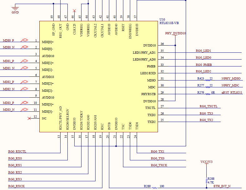
Figure 15.4 Schematics of RTL8211E-VB
The RTL8211E-VB chip is used to form a Gigabit Ethernet module on the experiment board. The schematics is shown in Figure 15.4. The PHY chip is connected to the FPGA by receiving and transmitting two sets of signals. The receiving group signal prefix is RG0_RX, and the transmitting group signal prefix is RG0TX, which is composed of a control signal CTL, a clock signal CK and four data signals 3-0. RG0_LED0 and RG0_LED1 are respectively connected to the network port yellow signal light and green signal light. At the same time, the FPGA can configure the PHY chip through the clock line NPHY_MDC and the data line NPHY_MDIO.
15.3.3 Program Design
- Configure IP address
Before verification (the default PC NIC is a Gigabit NIC, otherwise it needed to be replaced). PC IP address needs to be confirmed first. In the DOS command window, type ipconfig -all command to check it. Example is shown in Figure 15. 5.
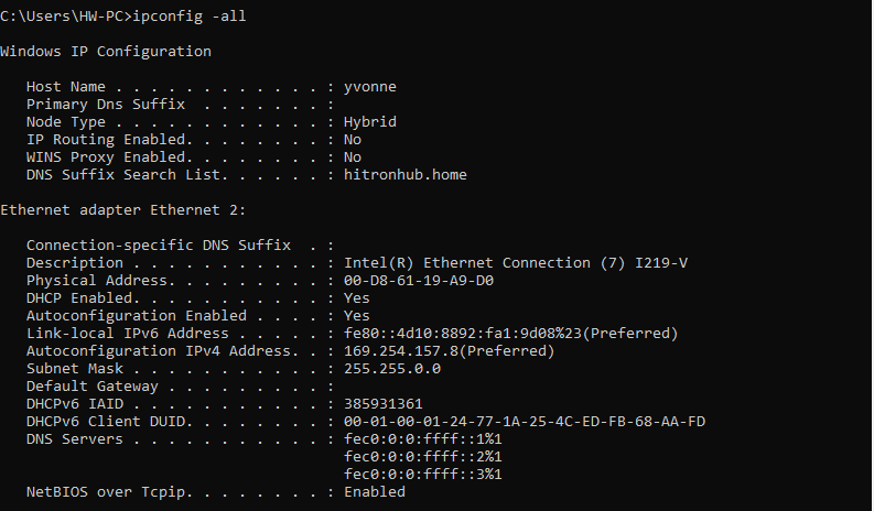
Figure 15.5 PC end IP information
To facilitate subsequent experiments, PC is provided a fixed IP address. Take this experiment as an example, IP configuration is 192.169.0.100(could be revised, but needs to be consistent to the IP address of target sending module, for Internet Protocol reason, IP address 169.XXX.X.X is not suggested). Find Internet Protocol Version 4(TCP/IPv4) in Network and Sharing center. See Figure 15. 6.
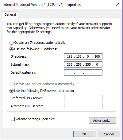
Figure 15.6 Configure PC end IP address
Since there is no ARP protocol content (binding IP address and MAC address of the develop board) in this experiment, it needs to be bound manually through the DOS command window. Here, the IP is set to 192.168.0.2 and the MAC address is set to 00-0A-35-01-FE-C0, (can be replaced by yourself) as shown in Figure 15. 7, the method is as follows: (Note: Run the DOS command window as an administrator)
Run the command: ARP -s 192.168.0.2 00-0A-35-01-FE-C0
View binding results: ARP -a
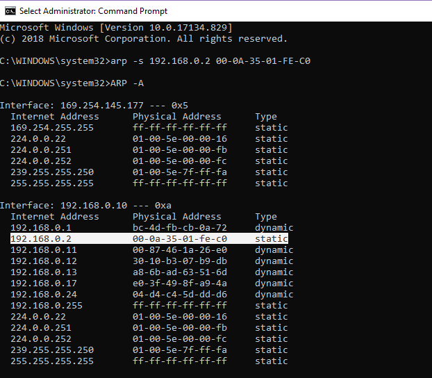
Figure 15.7 Address binding method 1
If a failure occurs while running the ARP command, another way is available, as shown in Figure 15.8:
- Enter the netsh i i show in command to view the number of the local connection, such as the “23” of the computer used this time.
- Enter netsh -c “i i” add neighbors 23 (number) “192.168.0.2” “00-0A-35-01-FE-C0”
- Enter arp -a to view the binding result
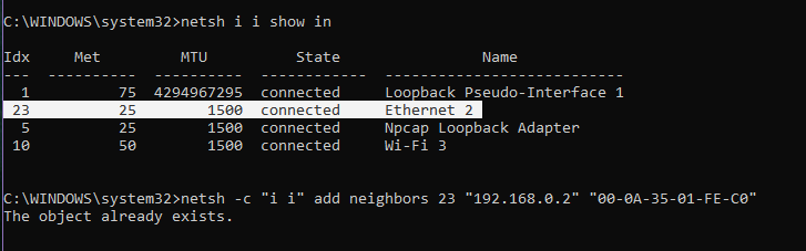
Figure 15.8 Address binding method 2
Next, we also use the DOS command window for connectivity detection, as shown in Figure 15. 9. Ping is an executable command that comes with the Windows family. Use it to check if the network can be connected. It can help us analyze and determine network faults. Application format: Ping IP address (not host computer IP).
Figure 15.9 Send data
- Loopback test design (test1)
The first step: introduction to the program
The loopback test only needs to output the input data directly. Refer project file loopback for more information. In the project, two IP cores, IDDR and ODDR, are used to complete the receiving and transmitting functions.
|
Because it is the RGMII interface, the data is bilateral along 4-bit data. Therefore, when data processing is performed inside the FPGA, it needs to be converted into 8-bit data. Go to PROJECT MANAGER > IP Catalog > SelectIO Interface Wizard to call the IP core(e_input_inst). SelectIO Interface Wizard is essentially composed of IDDR and ODDR. After internal data processing, IP core is passed (e_output_inst) to convert 8-bit data into bilateral edge 4-bit data transfer. It should be noted that, considering the enable signal and data signal synchronization, the enable signal is entered for conversion at the same time. The specific settings are shown in Figure 15. 11 and Figure 15. 12.
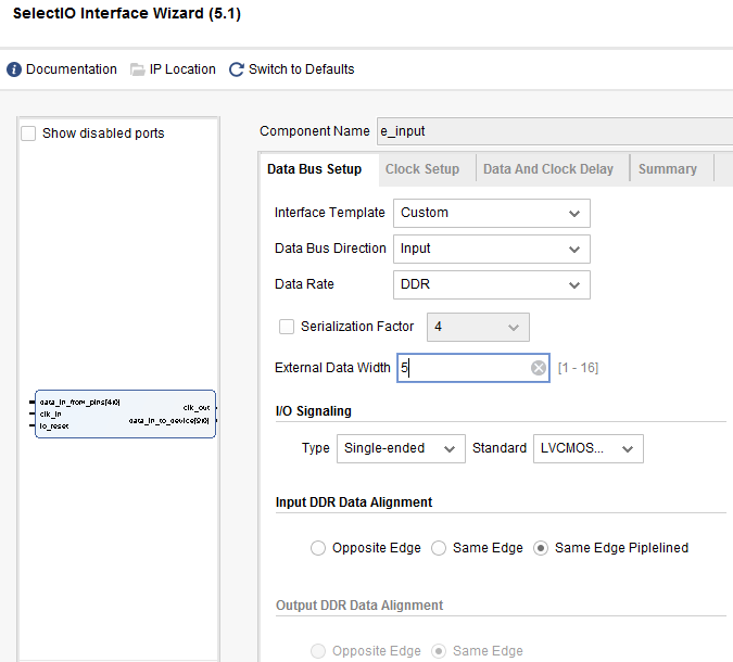
Figure 15.11 e_input_inst setting
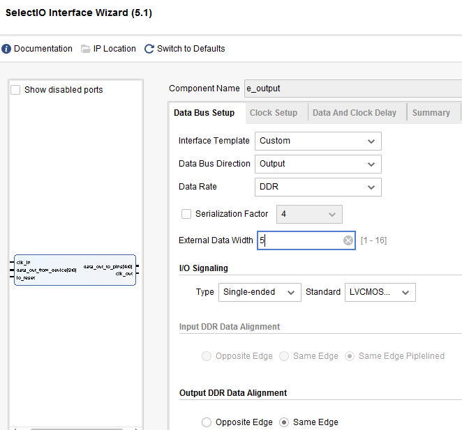
Figure 15.12 e_output_inst setting
When using the SelectIO Interface IP core as an output, it is necessary to meet its input timing, as shown in Figure 15.13. In the loopback test, the data is output by the e_intput_inst module, so the output clock rxc_r, which is clk_125m_90 after the PLL positively shifted by 90 degrees, as the output clock. Therefore, the clock and data input to e_output_inst will be 90 degrees different from each other to ensure the correctness of its output timing.
Figure 15.13 Input timing diagram of SelectIO Interface IP
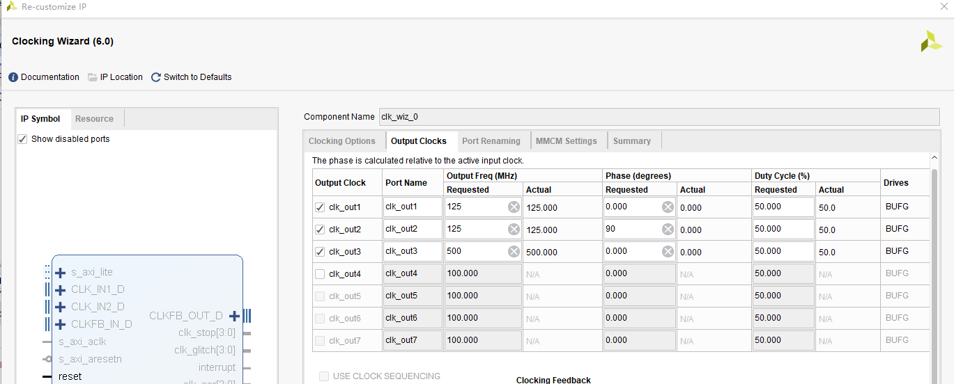
Figure 15.14 PLL output clock setting
After the three IP cores are instantiated, check the code synthesis and use the .xdc file to assign the pins.
(Note: each program in this experiment contains a smi_ctrl module. In the folder config, it is a module for setting the PHY chip, in order to solve the problem that some computers cannot connect to the network port normally, and will not be explained in detail for the moment)
The second step: assign th epins
See Table 15.1 for the pin assignment.
Table 15.1 Pin mapping
| Signal Name | Network Name | FPGA Pin | Port Description |
| rxck | RG0_RXCK | K21 | Input data clock |
| rxctl | RG0_RXCTL | M14 | Input data control signal |
| rx[3] | RG0_RX3 | J15 | 3rd bit input data |
| rx[2] | RG0_RX2 | J14 | 2nd bit input data |
| rx[1] | RG0_RX1 | K15 | 1st bit input data |
| rx[0] | RG0_RX0 | L14 | 0th bit input data |
| txck | RG0_TXCK | G20 | Output data clock |
| txctl | RG0_TXCTL | J16 | Output data control signal |
| tx[3] | RG0_TX3 | H19 | 3rd bit output data |
| tx[2] | RG0_TX2 | K18 | 2nd bit output data |
| tx[1] | RG0_TX1 | K17 | 1st bit output data |
| tx[0] | RG0_TX0 | K16 | 0th bit output data |
| e_mdio | NPHY_MDIO | J20 | Configure data |
| e_mdc | NPHY_MDC | F22 | Configure data |
As shown in Figure 15.15, after setting the correct address and data type, we send the detection information (love you!) through the host computer. The data packet is captured by Wireshark, as shown in Figure 15.16. The data is correctly transmitted back to the PC.
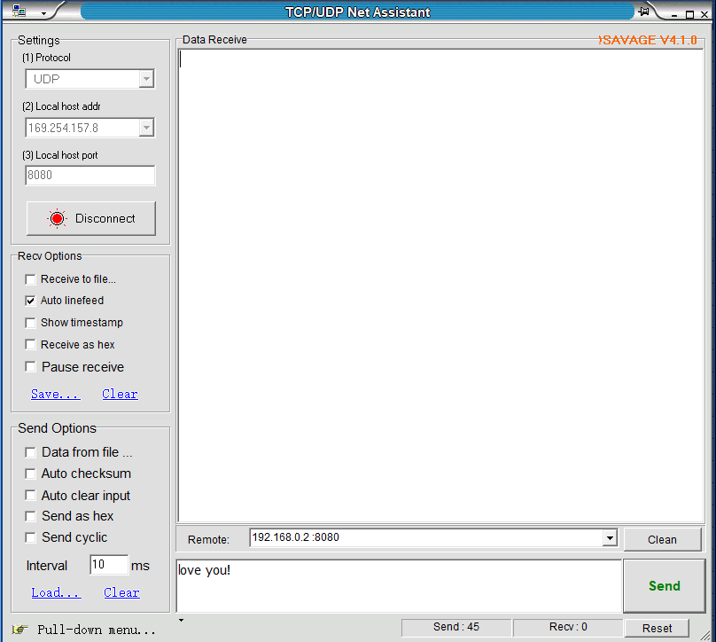
Figure 15.15 Host computer sends the test data
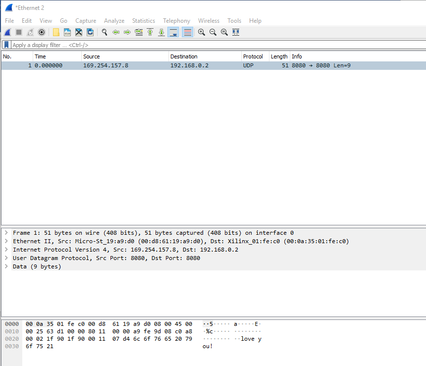
Figure 15.16 Correct reception of data on the PC side
(3)complete Ethernet data transmission design
For complete Ethernet data transmission, it is necessary to have the receiving part of the data and the transmitting part of the data. For the convenience of experiment, we store the data transmitted by the PC first in the RAM. After reading via the transmitting end, send it to the PC. For a series of data unpacking and packaging, refer to the project file “ethernet”. A brief introduction to each module follows.
- Data receiving module (ip_receive)
The problem to be solved by this module is to detect and identify the data frame, unpack the valid data frame, and store the real data in the ram.
|
The receiving module is to perform step by step analysis on the received data.
Idle state: If ‘55’ is received, it jumps to the six_55 state.
Six_55 state: If it continues to receive six consecutive 55s, it will jump to the spd_d5 state, otherwise it will return the idle state.
Spd_d5 state: If ‘d5’ continues received, it proves that the complete packet preamble “55_55_55_55_55_55_55_d5” has been received, and jumps to rx_mac, otherwise it returns the idle transition.
rx_mac state: This part is the judgment of the target MAC address and the source MAC address. If it matches, it will jump to the rx_IP_Protocol state, otherwise it will return the idle state and resend.
rx_IP_Protocol state: Determine the type and length of the packet and jump to the rx_IP_layer state.
rx_IP_layer state: Receive 20 bytes of UDP virtual header and IP address, jump to rx_UDP_layer state
rx_UDP_layer state: Receive 8-byte UDP port number and UDP packet length, jump to rx_data state
Rx_data state: Receive UDP data, jump to rx_finish state
Rx_finish state: A packet of data is received, and it jumps to the idle state to wait for the arrival of the next packet of data.
- Data sending module (ip_send)
The main content of this module is to read out the data in the RAM, package and transmit the data with the correct packet protocol type (UDP). Before transmitting, the data is also checked by CRC.
|
This part defines the preamble of the data packet, the MAC address of the PC, the MAC address of the development board, and the IP packet type. It should be noted that in the actual experiment, the MAC address of the PC needs to be modified. Keep the MAC address consistent along the project, otherwise the subsequent experiments will not receive data.
|
Idle state: Waiting for delay, sending a packet at regular intervals and jumping to the start state.
Start state: Send the packet header and jump to the make state.
make state: Generates the checksum of the header and jumps to the send55 state.
Send55 status: Send 8 preambles and jump to the sendmac state.
sendmac state: Send the target MAC address, source MAC address and IP packet type, and jump to the sendheader state.
sendheader state: Sends 7 32-bit IP headers and jumps to the senddata state.
senddata state: Send UDP packets and jump to the sendcrc state.
sendcrc state: Sends a 32-bit CRC check and returns the idle state.
Following the above procedure, the entire packet of data is transmitted, and the idle state is returned to wait for the transmission of the next packet of data.
- CRC check module (crc)
The CRC32 check of an IP packet is calculated at the destination MAC Address and until the last data of a packet. The CRC32 verilog algorithm and polynomial of Ethernet can be generated directly at the following website: http://www.easics.com/webtools/crctool
- UDP data test module (UDP)
This module only needs to instantiate the first three sub-modules together. Check the correctness of each connection.
- Top level module settings (ethernet)
The PLL, ddio_in, ddio_out, ram, and UDP modules are instantiated to the top level entity, and specific information is stored in advance in the RAM (Welcome To ZGZNXP World!). When there is no data input, the FPGA always sends this information. With data input, the received data is sent. Refer to the project files for more information.
15.4 Experiment Verification
The pin assignment of this test procedure is identical to that in loopback.
Before programming the development board, it is necessary to note that the IP address of the PC and the MAC address of the development board must be determined and matched, otherwise the data will not be received.
Download the compiled project to the development board. As shown in Figure 15.17, the FPGA is keeping sending information to the PC. The entire transmitted packet can also be seen in Wireshark, as shown in Figure 15.18.
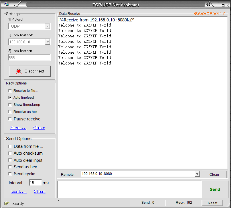
Figure 15.17 Send specific information
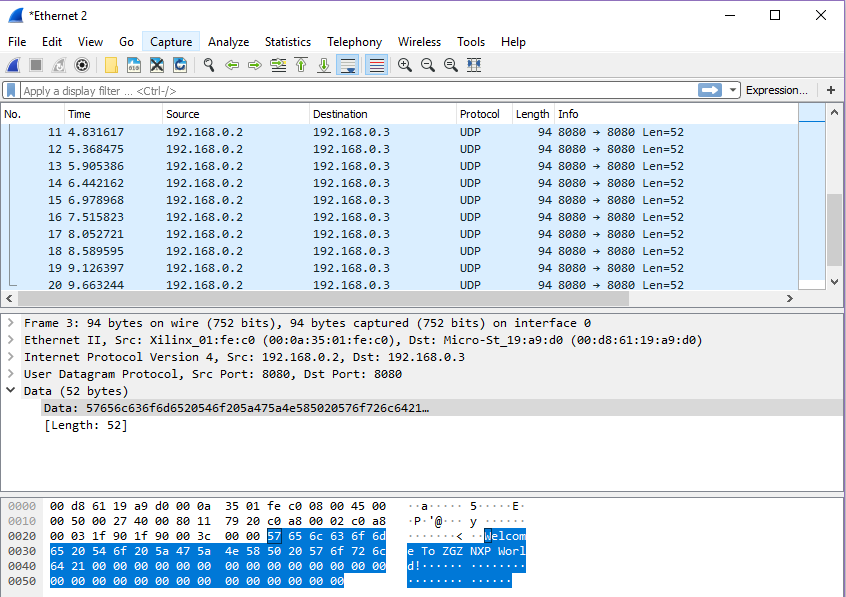
Figure 15.18 Specific information package
When the PC sends data to the FPGA, as shown in Figure 15. 19, the entire packet arrives at the FPGA, and then the FPGA repackages the received data and sends it to the PC. See Figure 15. 20, the network assistant also receives the transmitted data information accurately, as shown in Figure 15. 21.
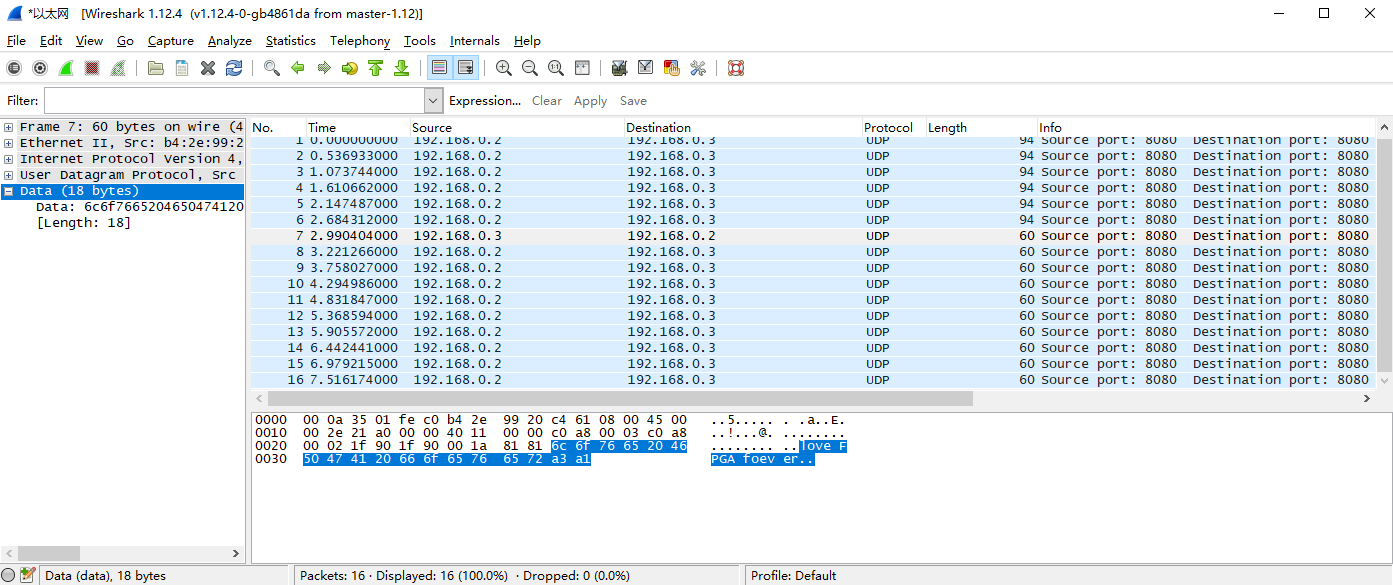
Figure 15.19 PC send data package

Figure 15.20 FPGA repackages the received data and sends it to the PC
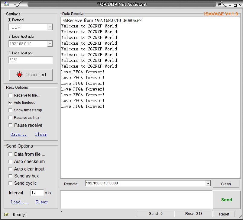
Figure 15.21 Information received by PC from FPGA
It should be noted that Ethernet II specifies the Ethernet frame data field is a minimum of 46 bytes, that is, the minimum Ethernet frame is 6+6+2+46+4=64. The 4-byte FCS is removed, so the packet capture is 60 bytes. When the length of the data field is less than 46 bytes, the MAC sublayer is padded after the data field to satisfy the data frame length of not less than 64 bytes. When communicating over a UDP LAN, “Hello World” often occurs for testing, but “Hello World” does not meet the minimum valid data (64-46) requirements. It is less than 18 bytes but the other party is still available for receiving, because data is complemented in the MAC sublayer of the link layer, less than 18 bytes are padded with ‘0’s. However, when the server is on the public network and the client is on the internal network, if less than 18 bytes of data is transmitted, the receiving end cannot receive the data. Therefore, if there is no data received, the information to be sent should be increased to more than 18 bytes.
Experiment 16 8978 Audio Loopback Experiment
16.1 Experiment Objective
- Learn about I2S (Inter-IC Sound) bus and how it works
- Familiar with the working mode of WM8978. And by configuring the interface mode and selecting the relevant registers in combination with the development board, complete the data transmission and reception, and verify it
16.2 Experiment Implement
- Perform audio loopback test by configuring the onboard audio chip WM8978 to check if the hardware is working properly
- Adjust the volume output level with the push buttons.
16.3 Experiment
16.3.1 WM8978 Introduction
WM8978 is a low power, high quality stereo multimedia digital signal CODEC introduced by Wolfson. It is mainly used in portable applications such as digital cameras and camcorders. Advanced on-chip digital signal processing includes a 5-band equaliser, a mixed signal Automatic Level Control for the microphone or line input through the ADC as well as a purely digital limiter function for record or playback. Additional digital filtering options are available in the ADC path, to cater for application filtering, such as “wind noise reduction”.
See Figure 16.1 for the internal structure block diagram of WM8978.
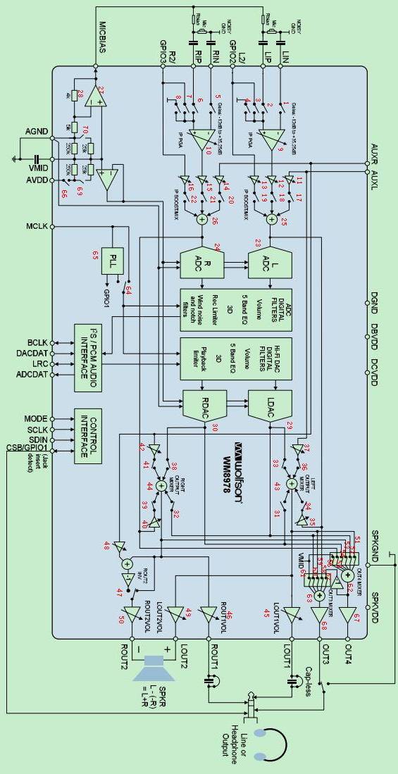
Figure 16.1 WM8978 internal structure block diagram
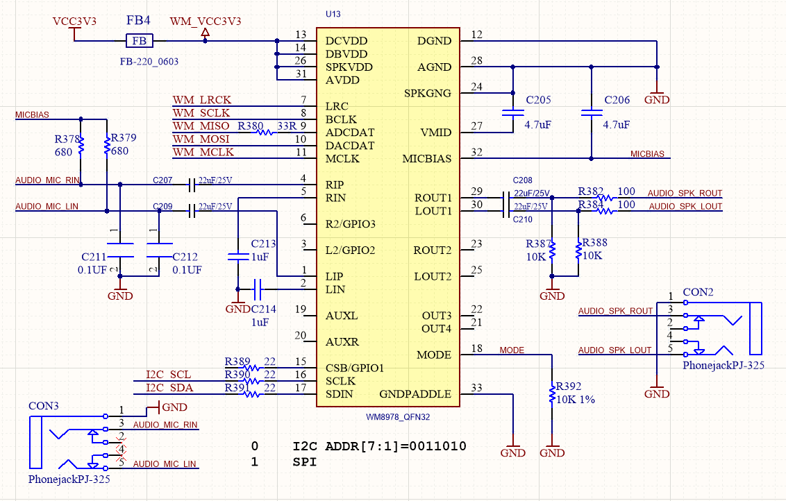
Figure 16.2 Schematics of the audio part of the development board
16.3.2 WM8978 Control Interface Timing
The WM8978 control interface has two-wire mode and three-wire mode. The specific mode is selected by the MODE pin connection of WM8978. When the mode pin is connected to a low voltage level, it is a two-wire mode, and when it is connected to a high voltage level, it is a three-wire mode. The development board mode pin is grounded. When the control interface is in two-wire mode, the timing diagram is shown in Figure 16.3. The timing diagram is the same as the IIC timing. The device address of WM8978 is fixed to 7’b0011010. This chip register only supports writing and does not support reading.
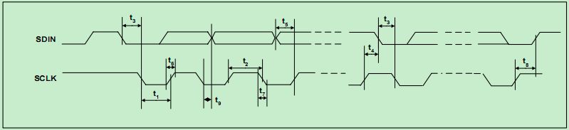
Figure 16.3 Timing diagram of the two-wire mode interface
16.3.3 I2S Audio Bus Protocol
I2S (Inter-IC Sound Bus) is just a branch of PCM, the interface definition is the same, I2S sampling frequency is generally 44.1KHz and 48KHz, PCM sampling frequency is generally 8K, 16K. There are four groups of signals: bit clock signal, synchronization signal, data input, data output.
I2S is a bus standard developed by Philips for audio data transmission between digital audio devices. In the Philips I2S standard, both the hardware interface specification and the format of digital audio data are specified. I2S has three main signals: the serial clock SCLK, also known as the bit clock BCLK, which corresponds to each bit of data of digital audio. The frequency of SCLK = 2 × sampling frequency × sampling number of bits. The frame clock LRCK is used to switch the data of the left and right channels. An LRCK of “0” indicates that data of the left channel is being transmitted, and “1” indicates that data of the right channel is being transmitted. LRCLK == FS, is the sampling frequency serial data SDATA, which is audio data expressed in two’s complement. Sometimes in order to enable better synchronization between systems, another signal MCLK is needed, which is called the master clock, or also called the system Clock (System Clock). It is 256 or 384 times the sampling frequency.
The timing of the I2S protocol is shown in Figure 16.4. However many bits of data the I2S format signal has, the most significant bit of the data always appears at the second BCLK pulse after the LRCK change (that is, the beginning of a frame). This allows the number of significant digits at the receiving end and the transmitting end to be different. If the receiving end can process less significant bits than the transmitting end, the extra low-order data in the data frame can be discarded; if the receiving end can process more significant bits than the transmitting end, it can make up the remaining bits by itself. This synchronization mechanism makes the interconnection of digital audio equipment more convenient without causing data errors.
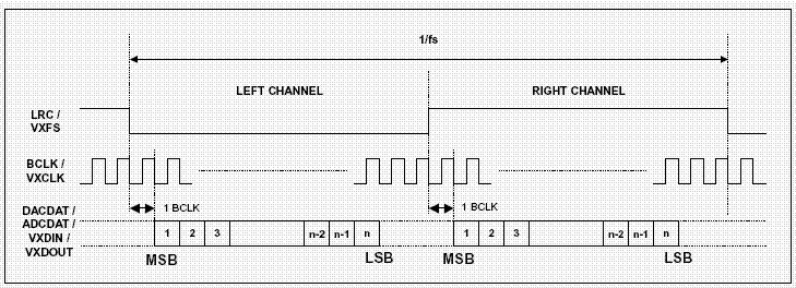
Figure 16.4 I2S timing protocol
16.3.4 Main Program Design
- WM8978 register configuration program
Only the program of register configuration program is given here, please refer to the project file for the complete program
|
- Audio signal acquisition program
|
- Audio sending module
|
- Main program
|
16.4 Experiment Verification
- Pin assignment
Table 16.1 Pin assignment
| Signal Name | Port Description | Network Name | FPGA Pin |
| Sys_clk_50 | System 50M clock | C10_50MCLK | U22 |
| Reset_n | System reset signal | KEY1 | M4 |
| Wm_sdin | 8978 register configuration data line | I2C_SDA | R21 |
| Wm_sclk | 8978 register configuration clock | I2C_SCL | R20 |
| Wm_lrc | 8978 align clock | WM_LRCK | H15 |
| Wm_bclk | 8978 bit clock | WM_BCLK | F18 |
| adcdat | ADC input of 8978 | WM_MISO | G19 |
| Dacdat | DAC input of 8978 | WM_MOSI | F20 |
| Mack | PLL provides 8978 working master clock | WM_MCLK | H17 |
| Key1 | Volume up button | Key2 | L4 |
| Key2 | Volume down button | Key7 | R7 |
| txd | Serial transmit | TTL_RX | L18 |
| rxd | Serial receive | TTL_TX | L17 |
- Board verification
As shown in Figure 16.5 below, after the FPGA development board is programmed, use a dual male audio cable, with one end plugged into the red audio receiver end and the other end plugged into a music player. Plug the headphone into the green audio playback port. The music can be heard from player. The volume is divided into 5 gears. Press the UP key to increase the volume and press the down key to decrease the volume.
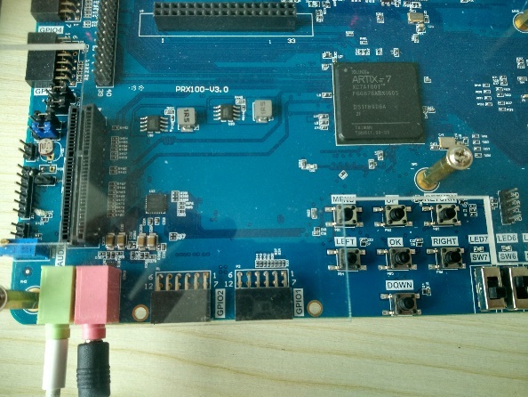
Figure 16.5 wm8978 board verification
Experiment 17 Reading Experiment of Serial Port Partition of Static Memory SRAM
17.1 Experiment Objective
- Learn about static memory SRAM read and write operations and how it works
- Familiar with the read and write timing of IS61WV25616BLL SRAM, and prepare for the next experimental experiment of OV5640 camera experiment.
17.2 Experiment Implement
- The experimental board is equipped with two pieces of SRAM, which are combined to form 18-bit address lines and 32-bit data spaces. After power-on, the FPGA will write the same value in the corresponding address in the entire memory space.
- The base address value of the SRAM is read and issued through the serial port, and then the stored data value corresponding to the base value space will be sent to the host computer through the serial port for display (the value corresponding to each base value interval).
17.3 Experiment
17.3.1 SRAM Introduction
SRAM (Static Random-Access Memory) is a type of random access memory. The “static” means that as long as the power is on, the data in the SRAM will remain unchanged. However, the data will still be lost after power turned off, which is the characteristics of the RAM.
Two SRAMs (IS61WV25616BLL) are on the development board, each SRAM has 256 * 16 words of storage space. Each word is 16-bit. The maximum read and write speed can reach 100 MHz. The physical picture is shown in Figure 17.1.
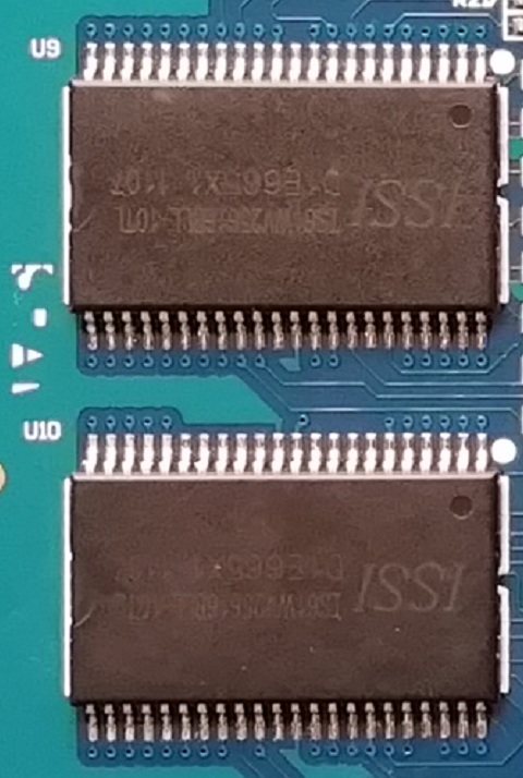
Figure 17.1 SRAM physical picture
17.3.2 Schematics
The schematics of the development board is shown in Figure 17.2: two pieces of SRAM share the same set of address lines to form a memory space with a bit width of 32 and a depth of 18 bits.
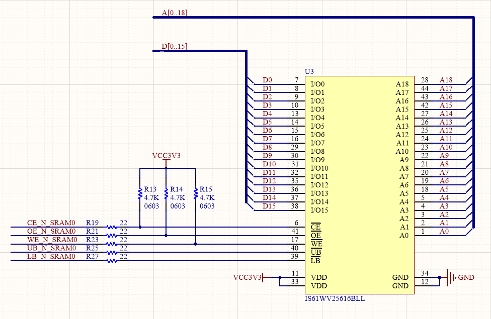
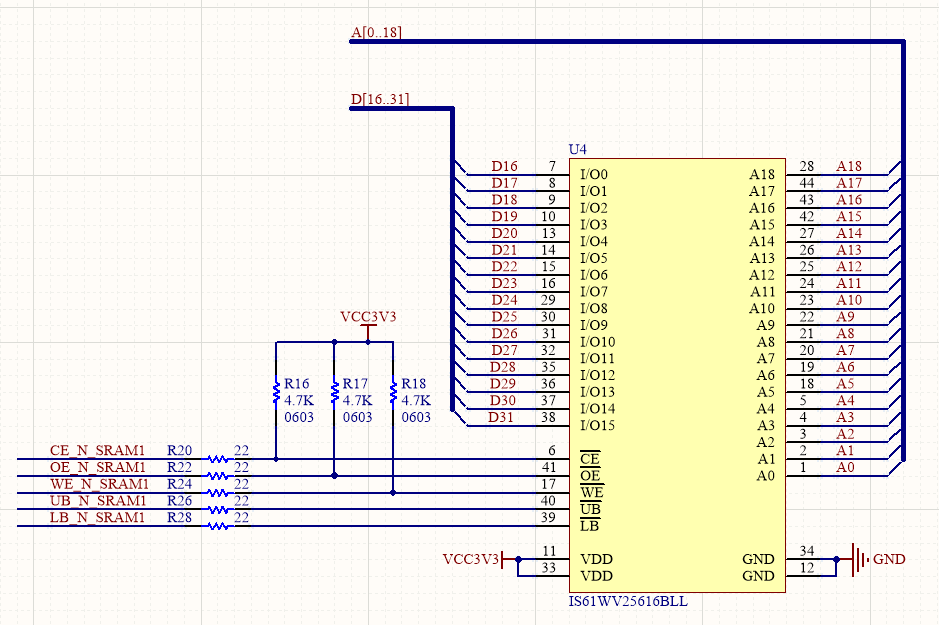
Figure 17.2 Schematics of SRAM0 and SRAM1
17.3.3 Main Program Design
The content of the serial port has been described before, and the core program is as follows:
- Sram controller design
From the official manual, there are two types of read timing for SRAM. The first read timing is used here as shown in Figure 17.3. Reading data is controlled by the Address bus
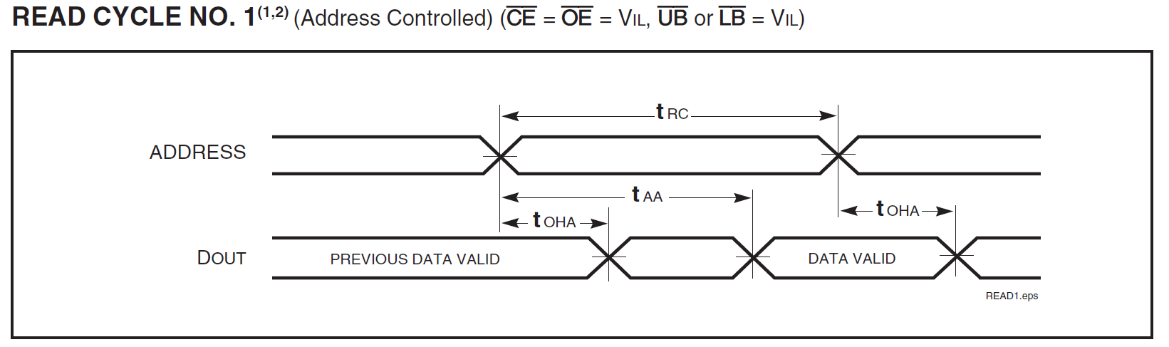
Figure 17.3 SRAM read timing
There are four types of write timing. The write timing used here is shown in Figure 17.4. The write control is controlled by the WE signal line.
Figure 17.4 SRAM write timing
The program is as follows:
| module sram_ctr (
input wire clk_50, input wire rst_n , input wire wr_en, input wire rd_en, input wire [17:0] sram_addr_wr_rd, input wire [31:0] data_we , output reg [31:0] data_rd, output reg data_valid=0 , output reg [17:0] sram_addr, inout [31:0] sram_data, output reg sram1_ce, output reg sram1_oe, output reg sram1_we, output reg sram1_lb, output reg sram1_ub, output reg sram0_ce, output reg sram0_oe, output reg sram0_we, output reg sram0_lb, output reg sram0_ub ) ; reg out_link=0; reg [31:0] sram_data_r; assign sram_data = out_link ? sram_data_r : 32’bz ; reg [1:0] sram_st=2’d0; always @ (posedge clk_50) begin if (~rst_n) begin sram_st <=2’d0; sram1_ce <=0; sram1_oe <=0; sram1_we <=1; sram1_lb <=0; sram1_ub <=0; sram0_ce <=0; sram0_oe <=0; sram0_we <=1; sram0_lb <=0; sram0_ub <=0; data_valid<=0 ; end else begin case (sram_st) 0 :begin sram1_ce <=0 ; sram1_oe <=0 ; sram1_we <=1 ; sram1_lb <=0 ; sram1_ub <=0 ; sram0_ce <=0 ; sram0_oe <=0 ; sram0_we <=1 ; sram0_lb <=0 ; sram0_ub <=0 ; data_valid<=0 ; sram_st<=1 ; end 1 : begin data_rd<=sram_data; data_valid<=0 ; out_link <=0 ; if (wr_en) begin sram1_we<=0; sram0_we<=0; sram_addr<=sram_addr_wr_rd; sram_data_r<= data_we ; out_link <=1 ; sram_st<=2 ; end if (rd_en) begin out_link <=0 ; sram1_we <=1; sram0_we <=1; sram_st<=3 ; sram_addr<=sram_addr_wr_rd; data_rd<=sram_data; end end 2 : begin sram1_we <=1; sram0_we <=1; sram_addr<=sram_addr_wr_rd; data_rd<=sram_data; sram_st<=1 ; end 3 : begin sram_addr<=sram_addr_wr_rd; data_rd<=sram_data; data_valid<=1 ; if (~rd_en) sram_st<=1; end default : sram_st<=0; endcase end end endmodule |
SRAM write data and read data program design: After the board is programmed, it will automatically write the value corresponding to the address from 0 to 18’h3ffff. The serial program issues the base address for reading the sram. All the data stored in the corresponding base address range will be returned and sent to the host computer through the serial port for display. (Here SRAM is divided into 8’h00 to 8’h3f base address spaces)
| module data_gen(
input wire sys_clk, input wire data_valid_rd , input wire rst_n, input wire rd_cmd, input wire [7:0] rd_cmd_addr, input tx_done , input [31:0] sramrd_data , output reg led =1, output [7:0] dout , output valid, output reg sram_rd_req, output reg sram_we_req , output reg [31:0] sram_data_we, output [17:0] sram_addr_we_rd ); reg rd_sign=0 ; reg [17:0] sram_addr_rd =0; reg [17:0] sram_addr_we =0 ; assign sram_addr_we_rd =led ?sram_addr_we: sram_addr_rd ; reg [18:0] wcnt; always @(posedge sys_clk) if (!rst_n)led<=1; else if (wcnt==19’h7FFFF) led<=0; else led<=led; always @ (posedge sys_clk,negedge rst_n) if (!rst_n) wcnt<=19’d0 ; else begin if (led) wcnt<=wcnt+1 ; else wcnt<=wcnt; end always @ (posedge sys_clk,negedge rst_n) if (!rst_n) begin sram_we_req <= 0 ; sram_data_we <=32’d0 ; sram_addr_we <=18’d0 ; end else begin if (led) begin if (!wcnt[0]) begin sram_we_req <= 1 ; sram_data_we <=sram_data_we ; sram_addr_we <=sram_addr_we ; end else begin sram_we_req <= 0 ; sram_data_we <=sram_data_we+1 ; sram_addr_we <=sram_addr_we +1; end end else begin sram_we_req <= 0 ; sram_data_we <=0 ; sram_addr_we <=0; end end reg [11:0] rdcnt =12’hfff; always @ (posedge sys_clk ,negedge rst_n) if (!rst_n) begin rdcnt<=12’hfff; sram_addr_rd <=18’d0 ; sram_rd_req <=0 ; rd_sign<=0 ; end else begin if(led==0) begin if (rd_cmd) begin rdcnt<=12’h000; sram_addr_rd<={rd_cmd_addr [5:0],12’h000}; sram_rd_req <=1 ; rd_sign<=1 ; end else begin if (rdcnt<12’hfff) begin rdcnt<=rdcnt+1; sram_addr_rd<=sram_addr_rd+1 ;end else begin rdcnt<=rdcnt;rd_sign<=0 ;if(rd_sign==0) sram_rd_req <=0 ; end end end else rdcnt<=12’hfff; end reg rd_en =0 ; wire [14 : 0] rd_data_count ; reg [1:0] cnt_cs =0 ; always @ (posedge sys_clk,negedge rst_n) if (!rst_n) begin rd_en <=0 ; cnt_cs<=2’b00 ; end else begin case (cnt_cs) 0: begin rd_en <=0 ; cnt_cs<=1 ; end 1: begin if (rd_data_count) begin rd_en <=1 ; cnt_cs<=2 ; end else begin rd_en <=0 ; cnt_cs<=1 ; end end 2: begin rd_en <=0 ; cnt_cs<=3 ; end 3: begin rd_en <=0 ; if (tx_done) cnt_cs<=0 ; else cnt_cs<=3 ; end endcase end fifo_sram your_instance_name ( .rst(!rst_n), // input wire rst .wr_clk(sys_clk), // input wire wr_clk .rd_clk(sys_clk), // input wire rd_clk .din(sramrd_data), // input wire [31 : 0] din .wr_en(data_valid_rd), // input wire wr_en .rd_en(rd_en), // input wire rd_en .dout(dout), // output wire [7 : 0] dout .full(), // output wire full .empty(empty), // output wire empty .valid(valid), // output wire valid .rd_data_count(rd_data_count), // output wire [14 : 0] rd_data_count .wr_rst_busy(), // output wire wr_rst_busy .rd_rst_busy() // output wire rd_rst_busy ); endmodule |
17.4 Board Verification
1 Pin assignment
Table 17.1 SRAM pin mapping
| Signal Name | Port Description | Network Name | FPGA Pin |
| Clk_50m | 50M system clock | C10_50MCLK | U22 |
| Sys_rst_n | System reset | KEY1 | M4 |
| Uart_rx | Serial receive | TTL_TX | L17 |
| Uart_tx | Serial transmit | TTL_RX | L18 |
| Sram_data[0] | SRAM data bus | D0 | U21 |
| Sram_data[1] | SRAM data bus | D1 | U25 |
| Sram_data[2] | SRAM data bus | D2 | W26 |
| Sram_data[3] | SRAM data bus | D3 | Y26 |
| Sram_data[4] | SRAM data bus | D4 | AA25 |
| Sram_data[5] | SRAM data bus | D5 | AB26 |
| Sram_data[6] | SRAM data bus | D6 | AA24 |
| Sram_data[7] | SRAM data bus | D7 | AB24 |
| Sram_data[8] | SRAM data bus | D8 | AC24 |
| Sram_data[9] | SRAM data bus | D9 | AC26 |
| Sram_data[10] | SRAM data bus | D10 | AB25 |
| Sram_data[11] | SRAM data bus | D11 | Y23 |
| Sram_data[12] | SRAM data bus | D12 | Y25 |
| Sram_data[13] | SRAM data bus | D13 | W25 |
| Sram_data[14] | SRAM data bus | D14 | V26 |
| Sram_data[15] | SRAM data bus | D15 | U26 |
| Sram_data[16] | SRAM data bus | D16 | T14 |
| Sram_data[17] | SRAM data bus | D17 | T17 |
| Sram_data[18] | SRAM data bus | D18 | W18 |
| Sram_data[19] | SRAM data bus | D19 | U17 |
| Sram_data[20] | SRAM data bus | D20 | V18 |
| Sram_data[21] | SRAM data bus | D21 | T18 |
| Sram_data[22] | SRAM data bus | D22 | W19 |
| Sram_data[23] | SRAM data bus | D23 | T19 |
| Sram_data[24] | SRAM data bus | D24 | W21 |
| Sram_data[25] | SRAM data bus | D25 | Y22 |
| Sram_data[26] | SRAM data bus | D26 | Y21 |
| Sram_data[27] | SRAM data bus | D27 | U20 |
| Sram_data[28] | SRAM data bus | D28 | T20 |
| Sram_data[29] | SRAM data bus | D29 | W20 |
| Sram_data[30] | SRAM data bus | D30 | Y20 |
| Sram_data[31] | SRAM data bus | D31 | V19 |
| Sram_addr[0] | SRAM address bus | A0 | E26 |
| Sram_addr[1] | SRAM address bus | A 1 | E25 |
| Sram_addr[2] | SRAM address bus | A 2 | D26 |
| Sram_addr[3] | SRAM address bus | A 3 | D25 |
| Sram_addr[4] | SRAM address bus | A 4 | G22 |
| Sram_addr[5] | SRAM address bus | A 5 | H18 |
| Sram_addr[6] | SRAM address bus | A 6 | M15 |
| Sram_addr[7] | SRAM address bus | A 7 | M16 |
| Sram_addr[8] | SRAM address bus | A 8 | L15 |
| Sram_addr[9] | SRAM address bus | A 9 | K23 |
| Sram_addr[10] | SRAM address bus | A 10 | J25 |
| Sram_addr[11] | SRAM address bus | A 11 | K22 |
| Sram_addr[12] | SRAM address bus | A 12 | H26 |
| Sram_addr[13] | SRAM address bus | A 13 | J26 |
| Sram_addr[14] | SRAM address bus | A 14 | J24 |
| Sram_addr[15] | SRAM address bus | A 15 | G25 |
| Sram_addr[16] | SRAM address bus | A 16 | G24 |
| Sram_addr[17] | SRAM address bus | A 17 | J21 |
| Sram_addr[18] | SRAM address bus | A 18 (invalid pin) | J23 |
| Sram0_cs_n | 0th SRAM enable | CE_N_SRAM0 | F25 |
| Sram0_we_n | 0th SRAM write enable | OE_N_SRAM0 | L19 |
| Sram0_oe_n | 0th SRAM read enable | WE_N_SRAM0 | H23 |
| Sram0_ub_n | 0th SRAM high byte enable | UE_N_SRAM0 | H24 |
| Sram0_lb_n | 0th SRAM low byte enable | LE_N_SRAM0 | G26 |
| Sram0_cs_n | 1st SRAM enable | CE_N_SRAM1 | E23 |
| Sram0_we_n | 1st SRAM write enable | OE_N_SRAM1 | J18 |
| Sram0_oe_n | 1st SRAM read enable | WE_N_SRAM1 | F23 |
| Sram0_ub_n | 1st SRAM high byte enable | UE_N_SRAM1 | F24 |
| Sram0_lb_n | 1st SRAM low byte enable | LE_N_SRAM1 | K20 |
2 Board Verification
After the FPGA development board is programmed. When led0 is on, it indicates that the program’s write operation to the SRAM is complete, and the SRAM can be read through the serial port. Serial port parameter setting: Baud rate: 9600, no parity. The following figure 17.4 shows the display result of the host computer reading the base address 8’h3f (base address range 8’h00 ~ 8’h3f). The data read out is one group per 4 bits. The green box is as follows: 0003F000, where 3F is the corresponding input base address. The next 3 digits are from 000 to FFF. The reception shows that the number of 2 to the power 12 times 4, which is equal to 16384. It indicates that the number of data read back is correct.
Figure 17.4 Result of reading the SRAM base address range by the serial port
Experiment 18 Photo Display Experiment of OV5640 Camera
18.1 Experiment Objective
- Understand the power-on sequence of the OV5640 camera and the corresponding register configuration process when outputting images of different resolutions
- Review previous knowledge of IIC bus
- Review previous knowledge of HDMI
18.2 Experiment Implement
- Read the power-on sequence of the OV5640 datasheet, and correctly write the power-on control program according to the peripheral module schematics.
- Correctly write the configuration program of the OV5640 camera with a resolution of 640X480 according to the timing requirements of the SCCB interface
- Based on previous experiments, write a program to store the image data collected by 5640 in the development board SRAM.
- Write a program to display the image stored in the SRAM to the monitor via HDMI.
- The refresh of the image is controlled by the keys, and the screen display image is updated every time pressing it, similar to a camera.
18.3 Experiment
Some main procedures are given below. Refer the project file for the complete program
- Ov5640 power-on initialization program design is based on the power-on timing diagram of 5640 when connected to DVDD. Shown in Figure 18.1.
Figure 18.1 5640 power-on sequence
Power-on sequence program is as follows:
| module power_on_delay(clk_50M,reset_n_r,camera_pwup,initial_en,cam_resetb);
input clk_50M; input reset_n_r; output camera_pwup; output initial_en; (*mark_debug=”true”*)output reg cam_resetb =0; (*mark_debug=”true”*)reg [31:0]cnt1=0; reg initial_en=0; reg camera_pwup_reg=0; reg reset_n =0; assign camera_pwup=camera_pwup_reg; always @ (posedge clk_50M) reset_n<=reset_n_r ; //5ms, delay from sensor power up stable to Pwdn pull down always@(posedge clk_50M) begin if(reset_n==1’b0) cnt1<=0; else begin if (cnt1<50000000) cnt1<=cnt1+1 ; else cnt1<=cnt1 ; end end always@(posedge clk_50M) begin if(reset_n==1’b0) begin camera_pwup_reg<=0; end else begin if (cnt1==15000000) camera_pwup_reg<=1; else camera_pwup_reg<=camera_pwup_reg; end end always@(posedge clk_50M) begin if(reset_n==1’b0) begin cam_resetb <=0; end else begin if (cnt1==35000000) cam_resetb <=1; else cam_resetb <=cam_resetb ; end end always@(posedge clk_50M) begin if(reset_n==1’b0) begin initial_en<=0; end else begin if (cnt1==48000000) initial_en<=1; else initial_en<=initial_en; end end endmodule |
- 5640 chip configuration program
After the development board is powered on correctly, the OV5640 related registers will be configured. The configuration of the OV5640 chip’s internal registers is performed through the SCCB (Serial Camera Control Bus) protocol. This protocol is equivalent to a simple I2C bus. The SCCB timing is shown in Figure 18.2. When configuring, use the I2C code from previous experiment directly.
18.2 SCCB write register timing diagram
The registers required to complete the 5640 camera function are as follows:
| always@(reg_index)
begin case(reg_index) 0:reg_data<=24’h310311; 1:reg_data<=24’h300882; 2:reg_data<=24’h300842; 3:reg_data<=24’h310303; 4:reg_data<=24’h3017ff; 5:reg_data<=24’h3018ff; 6:reg_data<=24’h30341A; 7:reg_data<=24’h303713; 8:reg_data<=24’h310801; 9:reg_data<=24’h363036; 10:reg_data<=24’h36310e; 11:reg_data<=24’h3632e2; 12:reg_data<=24’h363312; 13:reg_data<=24’h3621e0; 14:reg_data<=24’h3704a0; 15:reg_data<=24’h37035a; 16:reg_data<=24’h371578; 17:reg_data<=24’h371701; 18:reg_data<=24’h370b60; 19:reg_data<=24’h37051a; 20:reg_data<=24’h390502; 21:reg_data<=24’h390610; 22:reg_data<=24’h39010a; 23:reg_data<=24’h373112; 24:reg_data<=24’h360008; 25:reg_data<=24’h360133; 26:reg_data<=24’h302d60; 27:reg_data<=24’h362052; 28:reg_data<=24’h371b20; 29:reg_data<=24’h471c50; 30:reg_data<=24’h3a1343; 31:reg_data<=24’h3a1800; 32:reg_data<=24’h3a19f8; 33:reg_data<=24’h363513; 34:reg_data<=24’h363603; 35:reg_data<=24’h363440; 36:reg_data<=24’h362201; 37:reg_data<=24’h3c0134; 38:reg_data<=24’h3c0428; 39:reg_data<=24’h3c0598; 40:reg_data<=24’h3c0600; 41:reg_data<=24’h3c0708; 42:reg_data<=24’h3c0800; 43:reg_data<=24’h3c091c; 44:reg_data<=24’h3c0a9c; 45:reg_data<=24’h3c0b40; 46:reg_data<=24’h381000; 47:reg_data<=24’h381110; 48:reg_data<=24’h381200; 49:reg_data<=24’h370864; 50:reg_data<=24’h400102; 51:reg_data<=24’h40051a; 52:reg_data<=24’h300000; 53:reg_data<=24’h3004ff; 54:reg_data<=24’h300e58; 55:reg_data<=24’h302e00; 56:reg_data<=24’h430061; 57:reg_data<=24’h501f01; 58:reg_data<=24’h440e00; 59:reg_data<=24’h5000a7; 60:reg_data<=24’h3a0f30; 61:reg_data<=24’h3a1028; 62:reg_data<=24’h3a1b30; 63:reg_data<=24’h3a1e26; 64:reg_data<=24’h3a1160; 65:reg_data<=24’h3a1f14; 66:reg_data<=24’h580023; 67:reg_data<=24’h580114; 68:reg_data<=24’h58020f; 69:reg_data<=24’h58030f; 70:reg_data<=24’h580412; 71:reg_data<=24’h580526; 72:reg_data<=24’h58060c; 73:reg_data<=24’h580708; 74:reg_data<=24’h580805; 75:reg_data<=24’h580905; 76:reg_data<=24’h580a08; 77:reg_data<=24’h580b0d; 78:reg_data<=24’h580c08; 79:reg_data<=24’h580d03; 80:reg_data<=24’h580e00; 81:reg_data<=24’h580f00; 82:reg_data<=24’h581003; 83:reg_data<=24’h581109; 84:reg_data<=24’h581207; 85:reg_data<=24’h581303; 86:reg_data<=24’h581400; 87:reg_data<=24’h581501; 88:reg_data<=24’h581603; 89:reg_data<=24’h581708; 90:reg_data<=24’h58180d; 91:reg_data<=24’h581908; 92:reg_data<=24’h581a05; 93:reg_data<=24’h581b06; 94:reg_data<=24’h581c08; 95:reg_data<=24’h581d0e; 96:reg_data<=24’h581e29; 97:reg_data<=24’h581f17; 98:reg_data<=24’h582011; 99:reg_data<=24’h582111; 100:reg_data<=24’h582215; 101:reg_data<=24’h582328; 102:reg_data<=24’h582446; 103:reg_data<=24’h582526; 104:reg_data<=24’h582608; 105:reg_data<=24’h582726; 106:reg_data<=24’h582864; 107:reg_data<=24’h582926; 108:reg_data<=24’h582a24; 109:reg_data<=24’h582b22; 110:reg_data<=24’h582c24; 111:reg_data<=24’h582d24; 112:reg_data<=24’h582e06; 113:reg_data<=24’h582f22; 114:reg_data<=24’h583040; 115:reg_data<=24’h583142; 116:reg_data<=24’h583224; 117:reg_data<=24’h583326; 118:reg_data<=24’h583424; 119:reg_data<=24’h583522; 120:reg_data<=24’h583622; 121:reg_data<=24’h583726; 122:reg_data<=24’h583844; 123:reg_data<=24’h583924; 124:reg_data<=24’h583a26; 125:reg_data<=24’h583b28; 126:reg_data<=24’h583c42; 127:reg_data<=24’h583dce; 128:reg_data<=24’h5180ff; 129:reg_data<=24’h5181f2; 130:reg_data<=24’h518200; 131:reg_data<=24’h518314; 132:reg_data<=24’h518425; 133:reg_data<=24’h518524; 134:reg_data<=24’h518609; 135:reg_data<=24’h518709; 136:reg_data<=24’h518809; 137:reg_data<=24’h518975; 138:reg_data<=24’h518a54; 139:reg_data<=24’h518be0; 140:reg_data<=24’h518cb2; 141:reg_data<=24’h518d42; 142:reg_data<=24’h518e3d; 143:reg_data<=24’h518f56; 144:reg_data<=24’h519046; 145:reg_data<=24’h5191f8; 146:reg_data<=24’h519204; 147:reg_data<=24’h519370; 148:reg_data<=24’h5194f0; 149:reg_data<=24’h5195f0; 150:reg_data<=24’h519603; 151:reg_data<=24’h519701; 152:reg_data<=24’h519804; 153:reg_data<=24’h519912; 154:reg_data<=24’h519a04; 155:reg_data<=24’h519b00; 156:reg_data<=24’h519c06; 157:reg_data<=24’h519d82; 158:reg_data<=24’h519e38; 159:reg_data<=24’h548001; 160:reg_data<=24’h548108; 161:reg_data<=24’h548214; 162:reg_data<=24’h548328; 163:reg_data<=24’h548451; 164:reg_data<=24’h548565; 165:reg_data<=24’h548671; 166:reg_data<=24’h54877d; 167:reg_data<=24’h548887; 168:reg_data<=24’h548991; 169:reg_data<=24’h548a9a; 170:reg_data<=24’h548baa; 171:reg_data<=24’h548cb8; 172:reg_data<=24’h548dcd; 173:reg_data<=24’h548edd; 174:reg_data<=24’h548fea; 175:reg_data<=24’h54901d; 176:reg_data<=24’h53811e; 177:reg_data<=24’h53825b; 178:reg_data<=24’h538308; 179:reg_data<=24’h53840a; 180:reg_data<=24’h53857e; 181:reg_data<=24’h538688; 182:reg_data<=24’h53877c; 183:reg_data<=24’h53886c; 184:reg_data<=24’h538910; 185:reg_data<=24’h538a01; 186:reg_data<=24’h538b98; 187:reg_data<=24’h558006; 188:reg_data<=24’h558340; 189:reg_data<=24’h558410; 190:reg_data<=24’h558910; 191:reg_data<=24’h558a00; 192:reg_data<=24’h558bf8; 193:reg_data<=24’h501d40; 194:reg_data<=24’h530008; 195:reg_data<=24’h530130; 196:reg_data<=24’h530210; 197:reg_data<=24’h530300; 198:reg_data<=24’h530408; 199:reg_data<=24’h530530; 200:reg_data<=24’h530608; 201:reg_data<=24’h530716; 202:reg_data<=24’h530908; 203:reg_data<=24’h530a30; 204:reg_data<=24’h530b04; 205:reg_data<=24’h530c06; 206:reg_data<=24’h502500; 207:reg_data<=24’h300802; //680×480 30 frame/ second, night mode 5fps, input clock =24Mhz, PCLK =56Mhz 208:reg_data<=24’h303511; 209:reg_data<=24’h303646; 210:reg_data<=24’h3c0708; 211:reg_data<=24’h382047; 212:reg_data<=24’h382101; 213:reg_data<=24’h381431; 214:reg_data<=24’h381531; 215:reg_data<=24’h380000; 216:reg_data<=24’h380100; 217:reg_data<=24’h380200; 218:reg_data<=24’h380304; 219:reg_data<=24’h38040a; 220:reg_data<=24’h38053f; 221:reg_data<=24’h380607; 222:reg_data<=24’h38079b; 223:reg_data<=24’h380802; 224:reg_data<=24’h380980; 225:reg_data<=24’h380a01; 226:reg_data<=24’h380be0; 227:reg_data<=24’h380c07; 228:reg_data<=24’h380d68; 229:reg_data<=24’h380e03; 230:reg_data<=24’h380fd8; 231:reg_data<=24’h381306; 232:reg_data<=24’h361800; 233:reg_data<=24’h361229; 234:reg_data<=24’h370952; 235:reg_data<=24’h370c03; 236:reg_data<=24’h3a0217; 237:reg_data<=24’h3a0310; 238:reg_data<=24’h3a1417; 239:reg_data<=24’h3a1510; 240:reg_data<=24’h400402; 241:reg_data<=24’h30021c; 242:reg_data<=24’h3006c3; 243:reg_data<=24’h471303; 244:reg_data<=24’h440704; 245:reg_data<=24’h460b35; 246:reg_data<=24’h460c22; 247:reg_data<=24’h483722; 248:reg_data<=24’h382402; 249:reg_data<=24’h500183; 250:reg_data<=24’h350300; 251:reg_data<=24’h301602; 252:reg_data<=24’h3b070a; 253:reg_data<=24’h3b0083 ; 254:reg_data<=24’h3b0000 ; default:reg_data<=24’h000000; endcase end |
- The control codes for the LED control and camera functions are as follows:
|
- Some key codes to implement the camera function:
| module pic(
input wire key3 , (*mark_debug=”true”*)output reg hdmi_valid , (*mark_debug=”true”*)output reg [15:0] fifo_hdmi_dout , (*mark_debug=”true”*)input wire hdmi_rd_en , input wire hdmi_end , input wire hdmi_req , (*dont_touch=”true”, mark_debug=”true”*)output wire [10:0] hdmi_fifo_rd_data_count , output sram1_cs_n , output sram1_we_n , output sram1_oe_n , output sram1_ub_n , output sram1_lb_n , output sram0_cs_n , output sram0_we_n , output sram0_oe_n , output sram0_ub_n , output sram0_lb_n , output [17:0] sram_addr , inout [31:0] sram_data , input wire clk_50m , input wire rst_n_50m , input wire hdmi_reg_done , input wire reg_conf_done , input wire pic_clk , input wire vga_clk , (*mark_debug=”true”*)input wire camera_href , (*mark_debug=”true”*)input wire camera_vsync, (*mark_debug=”true”*)input wire [7:0] camera_data , (*mark_debug=”true”*)output led ); (*mark_debug=”true”*)reg camera_on = 0 ; reg lock_r = 0 ; (*mark_debug=”true”*)reg wr_en = 0 ; reg [7:0] din = 0 ; (*mark_debug=”true”*)reg rec_sign = 0 ; (*mark_debug=”true”*)reg sign_we = 0 ; (*mark_debug=”true”*)reg write_ack = 0 ; (*mark_debug=”true”*)reg [1:0] camera_vsync_rr =2’b00; (*dont_touch=”true”,mark_debug=”true”*)reg [11:0]camera_h_count; (*dont_touch=”true”,mark_debug=”true”*)reg [10:0]camera_v_count; assign led=!{camera_h_count,camera_v_count} ; always @ (posedge pic_clk) camera_vsync_rr <= {camera_vsync_rr[0],camera_vsync }; always @ (posedge pic_clk) if (hdmi_reg_done&(camera_vsync_rr==2’b10)&rst_n_50m&rec_sign) sign_we <=1 ; else if (camera_vsync_rr==2’b01) sign_we <=0 ; else sign_we <=sign_we ; //Generate camera line count always @(posedge pic_clk) begin if (!reg_conf_done) camera_h_count<=1; else if((camera_href==1’b1) & (camera_vsync==1’b0)) camera_h_count<=camera_h_count+1’b1; else camera_h_count<=1; end //Generate camera column count always @(posedge pic_clk) begin if (!reg_conf_done) camera_v_count<=0; else if (camera_vsync==1’b0) begin if(camera_h_count==1280) camera_v_count<=camera_v_count+1’b1; else camera_v_count<=camera_v_count; end else camera_v_count<=0 ; end always @ (posedge pic_clk) if (reg_conf_done==0) begin wr_en <=0 ; din <=0 ; end else begin if(camera_href&sign_we) begin wr_en <=1 ; din <=camera_data ; end else begin wr_en <=0 ; din <=0 ; end end (*mark_debug=”true”*) wire valid ; (*mark_debug=”true”*) wire [31: 0] dout ; (*mark_debug=”true”*) reg rd_en =0 ; (*mark_debug=”true”*) wire [9 : 0] rd_data_count ; wire [11 : 0] wr_data_count ; fifo_8_to_32 fifo_8_to_32_inst ( .rst(~rst_n_50m), // input wire rst .wr_clk(pic_clk), // input wire wr_clk .rd_clk(clk_50m), // input wire rd_clk .din(din), // input wire [7 : 0] din .wr_en(wr_en), // input wire wr_en .rd_en(rd_en), // input wire rd_en .dout(dout), // output wire [31 : 0] dout .full(), // output wire full .empty( ), // output wire empty .valid(valid), // output wire valid .rd_data_count(rd_data_count), // output wire [9 : 0] rd_data_count .wr_data_count(wr_data_count), // output wire [11 : 0] wr_data_count .wr_rst_busy( ), // output wire wr_rst_busy .rd_rst_busy( ) // output wire rd_rst_busy ); (*mark_debug=”true”*)reg [31:0] din_sram_fifo = 32’d0 ; (*mark_debug=”true”*)reg sram_fifo_wen = 0 ; (*mark_debug=”true”*)wire[15:0] fifo_hdmi_dout_r ; (*mark_debug=”true”*)wire hdmi_valid_r ; (*dont_touch=”true”,mark_debug=”true”*) wire [9:0] hdmi_fifo_wr_data_count ; (*dont_touch=”true”,mark_debug=”true”*) wire full ; (*dont_touch=”true”,mark_debug=”true”*) wire empty ; always @ (posedge vga_clk) begin fifo_hdmi_dout <= fifo_hdmi_dout_r ; hdmi_valid <= hdmi_valid_r ; end fifo_32_to_16 fifo_32_to_16_inst ( .rst(~rst_n_50m), // input wire rst .wr_clk(clk_50m), // input wire wr_clk .rd_clk(vga_clk), // input wire rd_clk .din(din_sram_fifo), // input wire [31 : 0] din .wr_en(sram_fifo_wen), // input wire wr_en .rd_en(hdmi_rd_en), // input wire rd_en .dout(fifo_hdmi_dout_r), // output wire [15 : 0] dout .full(full), // output wire full .empty(empty), // output wire empty .valid(hdmi_valid_r), // output wire valid .rd_data_count(hdmi_fifo_rd_data_count), // output wire [10 : 0] rd_data_count .wr_data_count(hdmi_fifo_wr_data_count), // output wire [9 : 0] wr_data_count .wr_rst_busy( ), // output wire wr_rst_busy .rd_rst_busy( ) // output wire rd_rst_busy ); reg [25:0] on_counter =26’d0 ; always @(posedge clk_50m , negedge reg_conf_done) if (!reg_conf_done) begin on_counter<=0; camera_on<=1’b0; end else begin if (key3==1’b1) // If the button is not pressed, the register is 0 on_counter<=0; else if ((key3==1’b0)& (on_counter<=500000)) // If the button is pressed and //held for less than 10ms, count on_counter<=on_counter+1’b1; if (on_counter==500000) // Once the button is effective, change the display mode camera_on<=1’b1; else if (write_ack ) camera_on<=1’b0; else camera_on<=camera_on; end (*mark_debug=”true”*) wire [31:0] data_rd ; (*mark_debug=”true”*) wire data_valid ; (*mark_debug=”true”*) reg [4:0] sram_wr_st = 0 ; (*mark_debug=”true”*) reg w_cnt = 0 ; (*mark_debug=”true”*) reg [17:0] sram_addr_wr_rd = 18’d0 ; (*mark_debug=”true”*) reg [31:0] data_we = 32’d0 ; (*mark_debug=”true”*) reg [31:0] rd_data = 32’d0 ; (*mark_debug=”true”*) reg wr_en_req = 0 ; (*mark_debug=”true”*) reg rd_en_req = 0 ; (*mark_debug=”true”*) reg [8:0] hdmi_req_cnt = 0 ; always @ (posedge clk_50m , negedge reg_conf_done ,negedge rst_n_50m ) begin if ( ~rst_n_50m|~reg_conf_done) begin rec_sign <= 0 ; sram_addr_wr_rd <= 18’d0 ; sram_wr_st <= 0 ; data_we <= 32’d0 ; rd_data <= 32’d0 ; wr_en_req <= 0 ; rd_en_req <= 0 ; hdmi_req_cnt <= 0 ; end else begin case ( sram_wr_st) 0 : begin rec_sign <= 0 ; sram_addr_wr_rd <= 18’d0 ; data_we <= 32’d0 ; rd_data <= 32’d0 ; wr_en_req <= 0 ; rd_en_req <= 0 ; sram_wr_st <= 1 ; write_ack <= 0 ; end 1 : begin if (camera_on) begin sram_wr_st <= 2 ; rec_sign <= 1 ; write_ack <= 1 ; end else sram_wr_st <= 7 ; end 2 : begin write_ack <= 0 ; if (sign_we) begin data_we <= 0 ; sram_addr_wr_rd <= 0 ; wr_en_req <= 0 ; rec_sign <= 0 ; sram_wr_st <= 3 ; end else begin rec_sign <= 1 ; sram_wr_st <= 2 ; end end 3 : begin if ( sign_we ) begin if ( rd_data_count ) begin rd_en <= 1 ; sram_wr_st <= 4 ; end else begin rd_en <= 0 ; sram_wr_st <= 3 ; end end else begin rd_en <= 0 ; sram_wr_st <= 0 ; end end 4 :begin rd_en <= 0 ; data_we <= dout ; sram_addr_wr_rd <= sram_addr_wr_rd ; wr_en_req <= valid ; sram_wr_st <= 5 ; end 5: begin data_we <= dout ; sram_addr_wr_rd <= sram_addr_wr_rd ; wr_en_req <= valid; sram_wr_st <= 6 ; end 6 : begin data_we <= dout ; sram_addr_wr_rd <= sram_addr_wr_rd +1 ; wr_en_req <= valid; sram_wr_st <= 3 ; end 7: begin din_sram_fifo <= data_rd ; sram_fifo_wen <= data_valid ; if (hdmi_end) sram_wr_st <= 0 ; else begin if (hdmi_req) begin rd_en_req <=1 ; sram_addr_wr_rd<=sram_addr_wr_rd; sram_wr_st <= 8 ; hdmi_req_cnt <= 0 ; end else begin hdmi_req_cnt <= 0 ; sram_wr_st <= 7 ; end end end 8: begin sram_addr_wr_rd<=sram_addr_wr_rd+1; sram_wr_st <= 9 ; end 9 :begin sram_addr_wr_rd <= sram_addr_wr_rd + 1 ; sram_wr_st <= 10 ; hdmi_req_cnt <= hdmi_req_cnt+1 ; end 10 : begin hdmi_req_cnt <= hdmi_req_cnt+1 ; din_sram_fifo <= data_rd ; sram_fifo_wen <= data_valid ; sram_addr_wr_rd<= sram_addr_wr_rd+1 ; if (hdmi_req_cnt==318) begin rd_en_req <= 0 ; sram_wr_st <= 7 ; end end default : sram_wr_st <= 0 ; endcase end end sram_ctr sram_ctr_inst0 ( .clk_50 (clk_50m ) , .rst_n (rst_n_50m ) , .wr_en (wr_en_req) , .rd_en (rd_en_req) , .sram_addr_wr_rd (sram_addr_wr_rd) , .data_we (data_we ) , .data_rd (data_rd ) , .data_valid (data_valid ) , .sram_addr (sram_addr) , .sram_data (sram_data) , .sram1_ce (sram1_cs_n) , .sram1_oe (sram1_oe_n) , .sram1_we (sram1_we_n) , .sram1_lb (sram1_lb_n) , .sram1_ub (sram1_ub_n) , .sram0_ce (sram0_cs_n) , .sram0_oe (sram0_oe_n) , .sram0_we (sram0_we_n) , .sram0_lb (sram0_lb_n) , .sram0_ub (sram0_ub_n) ) ; endmodule |
(4) For the HDMI part, refer to the relevant HDMI content in previous experiments
18.4 Experiment Board Verification
- Pin assignment table
| Signal Name | Port Description | Network Name | FPGA Pin |
| Clk_50m | System 50M clock | C10_50MCLK | U22 |
| Reset_n | System reset signal | KEY1 | M4 |
| Clk_24 | Clock procided by PLL to 5640 | IO29 | V14 |
| Camera_data[0] | 5640 imgae data bus | IO31 | V17 |
| Camera_data[1] | 5640 imgae data bus | IO27 | U16 |
| Camera_data[2] | 5640 imgae data bus | IO2 | AA22 |
| Camera_data[3] | 5640 imgae data bus | IO7 | V21 |
| Camera_data[4] | 5640 imgae data bus | IO5 | W23 |
| Camera_data[5] | 5640 imgae data bus | IO0 | U24 |
| Camera_data[6] | 5640 imgae data bus | IO26 | U15 |
| Camera_data[7] | 5640 imgae data bus | IO28 | U14 |
| Camera_pclk | 5640 image clock | IO1 | V24 |
| Camera_href | 5640 input horizontal signal | IO25 | T15 |
| Camera_vsync | 5640 input vertical signal | IO24 | U19 |
| Camera_pwup | 5640 power up control pin | IO6 | V22 |
| Key1 | Camera on | KEY3 | L8 |
| Key2 | LED | KEY6 | P1 |
| vga_hs | Horizontal synchronization signal | HDMI_HSYNC | C24 |
| vga_vs | Vertical synchronization signal | HDMI_VSYNC | A25 |
| en | Data valid | HDMI_DE | A24 |
| vga_clk | Display clock | HDMI_CLK | B19 |
| key1 | Display switch | KEY2 | L4 |
| scl | adv7511 configured clock | I2C_SCL | R20 |
| sda | adv7511 configured data line | I2C_SDA | R21 |
| vag_r[7] | Red output | HDMI_D23 | F15 |
| vag_r[6] | Red output | HDMI_D22 | E16 |
| vag_r[5] | Red output | HDMI_D21 | D16 |
| vag_r[4] | Red output | HDMI_D20 | G17 |
| vag_r[3] | Red output | HDMI_D19 | E17 |
| vag_r[2] | Red output | HDMI_D18 | F17 |
| vag_r[1] | Red output | HDMI_D17 | C17 |
| vag_r[0] | Red output | HDMI_D16 | A17 |
| vag_g[7] | Green output | HDMI_D15 | B17 |
| vag_g[6] | Green output | HDMI_D14 | C18 |
| vag_g[5] | Green output | HDMI_D13 | A18 |
| vag_g[4] | Green output | HDMI_D12 | D19 |
| vag_g[3] | Green output | HDMI_D11 | D20 |
| vag_g[2] | Green output | HDMI_D10 | A19 |
| vag_g[1] | Green output | HDMI_D9 | B20 |
| vag_g[0] | Green output | HDMI_D8 | A20 |
| vag_b[7] | Blue output | HDMI_D7 | B21 |
| vag_b[6] | Blue output | HDMI_D6 | C21 |
| vag_b[5] | Blue output | HDMI_D5 | A22 |
| vag_b[4] | Blue output | HDMI_D4 | B22 |
| vag_b[3] | Blue output | HDMI_D3 | C22 |
| vag_b[2] | Blue output | HDMI_D2 | A23 |
| vag_b[1] | Blue output | HDMI_D1 | D21 |
| vag_b[0] | Blue output | HDMI_D0 | B24 |
| Uart_rx | Serial receive | TTL_TX | L17 |
| Uart_tx | Serial transmit | TTL_RX | L18 |
| Sram_data[0] | SRAM data bus | D0 | U21 |
| Sram_data[1] | SRAM data bus | D1 | U25 |
| Sram_data[2] | SRAM data bus | D2 | W26 |
| Sram_data[3] | SRAM data bus | D3 | Y26 |
| Sram_data[4] | SRAM data bus | D4 | AA25 |
| Sram_data[5] | SRAM data bus | D5 | AB26 |
| Sram_data[6] | SRAM data bus | D6 | AA24 |
| Sram_data[7] | SRAM data bus | D7 | AB24 |
| Sram_data[8] | SRAM data bus | D8 | AC24 |
| Sram_data[9] | SRAM data bus | D9 | AC26 |
| Sram_data[10] | SRAM data bus | D10 | AB25 |
| Sram_data[11] | SRAM data bus | D11 | Y23 |
| Sram_data[12] | SRAM data bus | D12 | Y25 |
| Sram_data[13] | SRAM data bus | D13 | W25 |
| Sram_data[14] | SRAM data bus | D14 | V26 |
| Sram_data[15] | SRAM data bus | D15 | U26 |
| Sram_data[16] | SRAM data bus | D16 | T14 |
| Sram_data[17] | SRAM data bus | D17 | T17 |
| Sram_data[18] | SRAM data bus | D18 | W18 |
| Sram_data[19] | SRAM data bus | D19 | U17 |
| Sram_data[20] | SRAM data bus | D20 | V18 |
| Sram_data[21] | SRAM data bus | D21 | T18 |
| Sram_data[22] | SRAM data bus | D22 | W19 |
| Sram_data[23] | SRAM data bus | D23 | T19 |
| Sram_data[24] | SRAM data bus | D24 | W21 |
| Sram_data[25] | SRAM data bus | D25 | Y22 |
| Sram_data[26] | SRAM data bus | D26 | Y21 |
| Sram_data[27] | SRAM data bus | D27 | U20 |
| Sram_data[28] | SRAM data bus | D28 | T20 |
| Sram_data[29] | SRAM data bus | D29 | W20 |
| Sram_data[30] | SRAM data bus | D30 | Y20 |
| Sram_data[31] | SRAM data bus | D31 | V19 |
| Sram_addr[0] | SRAM address bus | A0 | E26 |
| Sram_addr[1] | SRAM address bus | A 1 | E25 |
| Sram_addr[2] | SRAM address bus | A 2 | D26 |
| Sram_addr[3] | SRAM address bus | A 3 | D25 |
| Sram_addr[4] | SRAM address bus | A 4 | G22 |
| Sram_addr[5] | SRAM address bus | A 5 | H18 |
| Sram_addr[6] | SRAM address bus | A 6 | M15 |
| Sram_addr[7] | SRAM address bus | A 7 | M16 |
| Sram_addr[8] | SRAM address bus | A 8 | L15 |
| Sram_addr[9] | SRAM address bus | A 9 | K23 |
| Sram_addr[10] | SRAM address bus | A 10 | J25 |
| Sram_addr[11] | SRAM address bus | A 11 | K22 |
| Sram_addr[12] | SRAM address bus | A 12 | H26 |
| Sram_addr[13] | SRAM address bus | A 13 | J26 |
| Sram_addr[14] | SRAM address bus | A 14 | J24 |
| Sram_addr[15] | SRAM address bus | A 15 | G25 |
| Sram_addr[16] | SRAM address bus | A 16 | G24 |
| Sram_addr[17] | SRAM address bus | A 17 | J21 |
| Sram_addr[18] | SRAM address bus | A 18 (invalid pin) | J23 |
| Sram0_cs_n | 0th SRAM enable | CE_N_SRAM0 | F25 |
| Sram0_we_n | 0th SRAM write enable | OE_N_SRAM0 | L19 |
| Sram0_oe_n | 0th SRAM read enable | WE_N_SRAM0 | H23 |
| Sram0_ub_n | 0th SRAM high byte enable | UE_N_SRAM0 | H24 |
| Sram0_lb_n | 0th SRAM low byte enable | LE_N_SRAM0 | G26 |
| Sram0_cs_n | 1st SRAM enable | CE_N_SRAM1 | E23 |
| Sram0_we_n | 1st SRAM write enable | OE_N_SRAM1 | J18 |
| Sram0_oe_n | 1st SRAM read enable | WE_N_SRAM1 | F23 |
| Sram0_ub_n | 1st SRAM high byte enable | UE_N_SRAM1 | F24 |
| Sram0_lb_n | 1st SRAM low byte enable | LE_N_SRAM1 | K20 |
| Led0 | OV5640 register configuration indicator | LED0 | N17 |
| Led1 | ADV7511 register configuration indicator | LED1 | M19 |
- Board verification
After the board is programmed, led0 and led1 light up, indicating that the OV5640 and ADV7511 configurations are complete.
Push button RIGHT has the function of turning on and off the LED fill light.
Press the RETURN button once, the camera will take a picture and display it on the display screen of the HDMI interface. Actual board test results are shown in Figure 18.3.
Figure 18.3a 5640 taken image Figure 18.3b 5640 display shows taken picture
Experiment 19 High-speed ADC9226 Acquisition Experiment
19.1 Experiment Objective
Learn about parallel ADC collectors and master the use of ADC9226.
19.2 Experiment Implement
1. Insert the ADC9226 module face up into the FPGA development board to the GPIO2 and GPIO1 ports which are next to the red-green audio module. Write programs to use this module to test
19.3 Experiment
19.3.1 ADC9226 Module Introduction
ADC9226 module adopts AD9226 chip design of ADI Company. This chip is a monolithic, 12-bit, 65 MSPS analog-to-digital converter (ADC). It uses a single power supply and has an on-chip high-performance sample-and-hold amplifier and voltage reference. It uses a multistage differential pipelined architecture with a data rate of 65 MSPS and guarantees no missing codes over the full operating temperature range.
See Figure 19.1 for ADC9226 timing diagram.
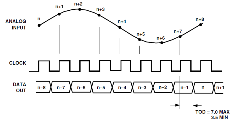
Figure19.1 ADC9226 timing diagram
From this timing diagram, we know that there is no need to configure the AD9226 chip, as long as the appropriate CLOCK is provided, the chip can perform data acquisition.
19.3.2 Program Design
-
- AD acquisition sub-module
As can be seen from Figure 19.1, the high bit of AD9226 is bit[0] and the low bit is bit [11], so the data bit order needs to be reversed in the program.
|
2.Data conversion program
The AD9226 module design uses an internal reference source. VREF is the output port of the reference source, which can be used for 1V and 2V reference voltages. It can be selected through SENCE. When SENCE is grounded, a 2V reference is provided, and when SENCE is connected to VREF, a 1V reference is provided. The module uses a 2V reference power supply. VINA input range is 1.0 ~ 3.0V.
The 22 pin of AD9226 has the function of collecting data selection. There are two input and output data formats of AD9226. For the specific format, refer to the 9226 datasheet. The 22 pin of the AD9226 module in this experiment is connected to high level, so it uses Binary Output Mode. The BCD conversion submodule has been introduced in Experiment 8 and is not repeated here.
| module volt_cal(
input wire ad_clk, input wire [11:0] ad_ch1, output [19:0] ch1_dec, output reg ch1_sig ); reg [31:0] ch1_data_reg; reg [11:0] ch1_reg; reg [31:0] ch1_vol; always @(posedge ad_clk) begin if(ad_ch1[11]==1’b1) begin ch1_reg<={1’b0,ad_ch1[10:0]}; ch1_sig <= 0; end else begin ch1_reg<={12’h800-ad_ch1[10:0]}; ch1_sig<=1; end end always @(posedge ad_clk) begin ch1_data_reg<=ch1_reg * 2000; ch1_vol<=ch1_data_reg >>11; end bcd bcd1_ist( .hex (ch1_vol[15:0]), .dec (ch1_dec), .clk (ad_clk) ); endmodule |
- 9226 module AD acquisition range selection
The attenuation range of the AD acquisition module is divided into gears. Press the UP key on the development board to switch the range.
Table 19.1 Gear shift indication table
| Gear comparison table (input voltage percentage) | Corresponding indicator |
| 4% | led0 lit |
| 8% | led0, led1 lit |
| 20% | led0, led1, led2 lit |
| 40% | led0, led1, led2, led2 lit |
|
- Main program design
The main program is divided into three sub-programs, which are AD_9226 acquisition module, data conversion calculation module volt_cal, and voltage value segment display module. The segment display part has been introduced in the previous experiment and will not be introduced here.
|
|
19.4 Experiment Verification
- Pin assignment
| Signal Name | Port Description | Network Name | FPGA Pin |
| sys_clk | System clock | C10_50MCLK | U22 |
| sys_rst_n | System reset | KEY1 | M4 |
| lg_en | ADG612 input | IO25 | T15 |
| hg_en | ADG612 input | IO24 | U19 |
| ad1_clk | Ad acquisition clock | IO28 | V14 |
| otr | Input voltage overrange flag | IO1 | V24 |
| sm_db[0] | Segment selection | SEG_PA | K26 |
| sm_db[1] | Segment selection | SEG_PB | M20 |
| sm_db[2] | Segment selection | SEG_PC | L20 |
| sm_db[3] | Segment selection | SEG_PD | N21 |
| sm_db[4] | Segment selection | SEG_PE | N22 |
| sm_db[5] | Segment selection | SEG_PF | P21 |
| sm_db[6] | Segment selection | SEG_PG | P23 |
| sm_db[7] | Segment selection | SEG_DP | P24 |
| sel[0] | Bit selection | SEG_3V3_D0 | R16 |
| sel[1] | Bit selection | SEG_3V3_D1 | R17 |
| sel[2] | Bit selection | SEG_3V3_D2 | N18 |
| sel[3] | Bit selection | SEG_3V3_D3 | K25 |
| sel[4] | Bit selection | SEG_3V3_D4 | R25 |
| sel[5] | Bit selection | SEG_3V3_D5 | T24 |
| ad1_in[0] | AD9226 acquisition data bus | IO0 | U24 |
| ad1_in[1] | AD9226 acquisition data bus | IO5 | W23 |
| ad1_in[2] | AD9226 acquisition data bus | IO4 | V23 |
| ad1_in[3] | AD9226 acquisition data bus | IO3 | AA23 |
| ad1_in[4] | AD9226 acquisition data bus | IO6 | V22 |
| ad1_in[5] | AD9226 acquisition data bus | IO2 | AA22 |
| ad1_in[6] | AD9226 acquisition data bus | IO7 | V21 |
| ad1_in[7] | AD9226 acquisition data bus | IO29 | U14 |
| ad1_in[8] | AD9226 acquisition data bus | IO30 | V16 |
| ad1_in[9] | AD9226 acquisition data bus | IO31 | V17 |
| ad1_in[10] | AD9226 acquisition data bus | IO27 | U16 |
| ad1_in[11] | AD9226 acquisition data bus | IO26 | U15 |
- Board verification
Use 1M sine wave as the signal source, AD9226 module to connect to GPIO1 and GPIO2 of 100T. Use the logic analyzer to capture the signal as shown in Figure 19.2.From the left to the right of the segment display, the first segment display is selected and lit to indicate that the input measurement voltage exceeds the AD9226 measurement range (the absolute value of VINA-VINB is less than or equal to the reference voltage, and the reference voltage of this module is 2V). The second segment display shows the sign of the input voltage (VINA-VINB). The last four digits are the input voltage value. When the input signal value is a slowly changing signal, the segment display can display the signal voltage amplitude.
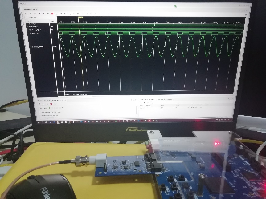
Figure 19.2 Signal waveform of AD9226 captured by logic analyzer
Experiment 20 DAC9767 DDS Signal Source Experiment
20.1 Experiment Objective
- Learn about DDS (Direct Digital Synthesizer) related theoretical knowledge.
- Read the AD9767 datasheet and use the AD9767 to design a signal source that can generate sine, square, triangle, and sawtooth waves.
20.2 Experiment Implement
- Learn about DDS theoretical knowledge.
- On the basis of understanding the principle of DDS, combined with the theoretical knowledge, use AD9767 module and development board to build a signal source whose waveform, amplitude and frequency can be adjusted. (There are no specific requirements for the adjustment of waveform, amplitude, and frequency here, as long as the conversion can be adjusted by pressing a button).
20.3 Experiment
20.3.1 DDS Introduction
The DDS technology is based on the Nyquist sampling theorem. Starting from the phase of the continuous signal, the sine signal is sampled, encoded, and quantized to form a sine function table, which is stored in the ROM. During synthesis, phase increment is changed by changing the frequency word of the phase accumulator. Phase increment is what is called step size. The difference in phase increment results in different sampling points in a cycle. When the clock frequency, or the sampling frequency does not change, the frequency is changed by changing the phase. The block diagram is shown in Figure 20.1.
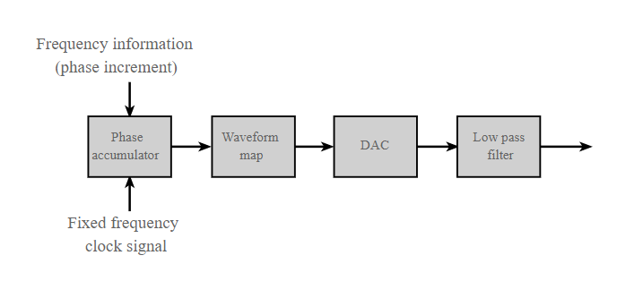
Figure 20.1 DDS block diagram
20.3.2 AD9767 Configuration Introduction
The AD9767 module uses ADI’s AD9767 DAC chip, which is a 14-bit, 125MSPS conversion rate high-performance DAC device. It supports the IQ output mode and can be used in the communications.
AD9767 interface timing requirements. As shown in Figure 20.2 below, when the rising edge of the clock comes, the data must remain stable for ts time. After the rising edge of the clock, the data must remain stable for th to be correct.
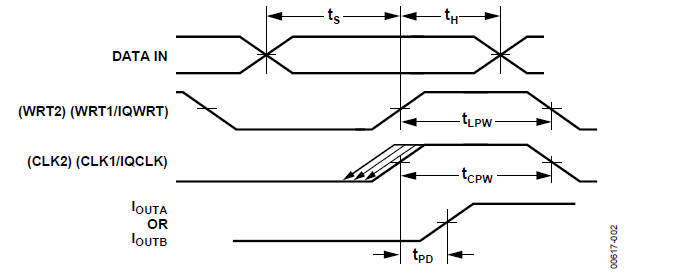
Figure 20.2 9767 interface timing diagram
20.3.3 Waveform Memory File Configuration
The waveform storage area file is dds_4096x10b_wave_init.coe. For the specific making process, refer to the use of the *.coe file in the experiment 9. The file containing the waveform information is stored in the ROM. After the project file is programmed into the FPGA, the FPGA directly reads the waveform information from the ROM and sends it to the AD9767 interface, and then outputs the corresponding waveform on the AD9767 module. The waveform storage is as shown in Figure 20.3.
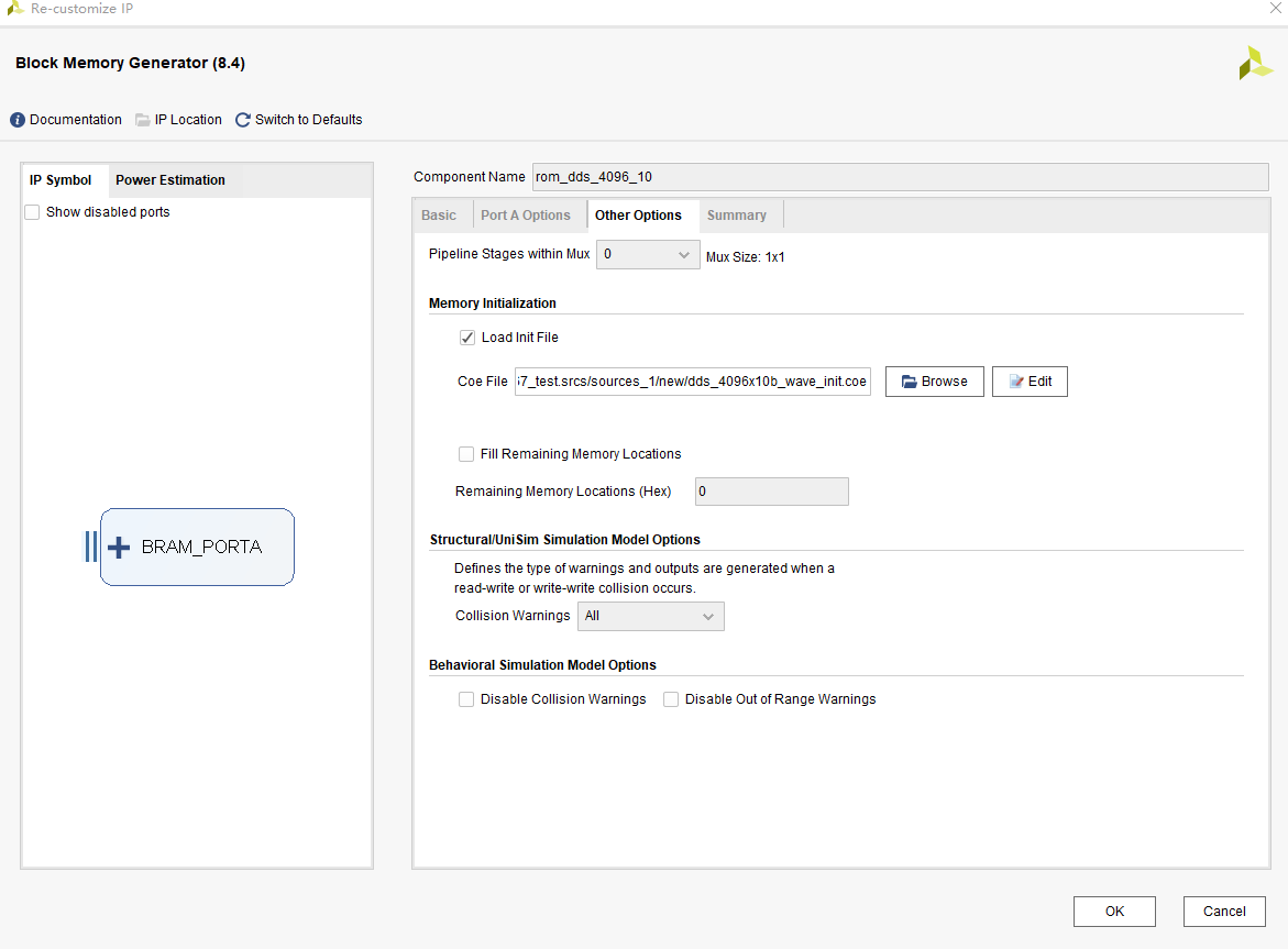
Figure 20.3 Wave file storage
20.3.4 Program Design
1. The main program includes waveform selection, mode selection, frequency adjustment, and amplitude adjustment. The specific code is as follows:
|
20.4 Experiment Varification
1. Pin assignment
| Signal Name | Port Description | Network Name | FPGA Pin |
| sys_clk_50m | System clock | C10_50MCLK | U22 |
| mode | 9767mode control | IO24 | U19 |
| wave_adjust | Waveform selection | key2 | L4 |
| a_adjust | Amplitude selection | key3 | L5 |
| f_adjust | Frequency selection | key4 | K5 |
| mode_adjust | Mode selection | key6 | P1 |
| led | Mode indicator light | LED0 | N17 |
| dac_clk | 9767 driving clock | IO28 | U14 |
| rst_n | System reset | key1 | M4 |
| data_out[0] | AD9767 data bus | IO1 | V24 |
| data_out[1] | AD9767 data bus | IO0 | U24 |
| data_out[2] | AD9767 data bus | IO5 | W23 |
| data_out[3] | AD9767 data bus | IO4 | V23 |
| data_out[4] | AD9767 data bus | IO3 | AA23 |
| data_out[5] | AD9767 data bus | IO6 | V22 |
| data_out[6] | AD9767 data bus | IO2 | AA22 |
| data_Out[7] | AD9767 data bus | IO7 | V21 |
| data_out[8] | AD9767 data bus | IO29 | V14 |
| data_out[9] | AD9767 data bus | IO30 | V16 |
| data_out[10] | AD9767 data bus | IO31 | V17 |
| data_out[11] | AD9767 data bus | IO27 | U16 |
| data_out[12] | AD9767 data bus | IO26 | U15 |
| data_out[13] | AD9767 data bus | IO25 | T15 |
2. Board verification
After the FPGA development board is programmed, press the right key (mode), and the mode indicator led0 lights up.
Then waveform can be chosen according to UP key (waveform selection), RETURN key (amplitude selection), LEFT key (frequency selection). (This experiment is only to introduce the theoretical knowledge of DDS and verify its correctness. Therefore, only four types of waveforms are set, which are sine wave, square wave, triangle wave, and sawtooth wave. The frequency and amplitude are also randomly set.) Figure 20.4 below shows four waveforms of the oscilloscope measuring the output of the 9767 module.
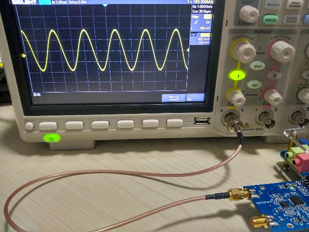
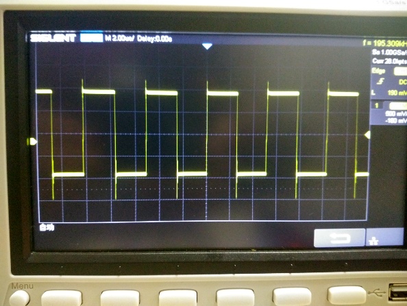
Figure 20-4a Sine wave Figure 20-4b Square wave
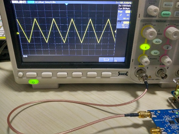
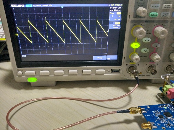
Figure 20-4c Triangle wave Figure 20-4d Sawtooth wave
References
-
- http://web.engr.oregonstate.edu/~traylor/ece474/beamer_lectures/verilog_operators.pdf
- https://www.utdallas.edu/~akshay.sridharan/index_files/Page5212.htm
- https://www.xilinx.com/support/documentation/sw_manuals/xilinx2015_2/ug908-vivado-programming-debugging.pdf
- https://www.xilinx.com/support/documentation/sw_manuals/xilinx2016_4/ug835-vivado-tcl-commands.pdf#nameddest=xwrite_cfgmem