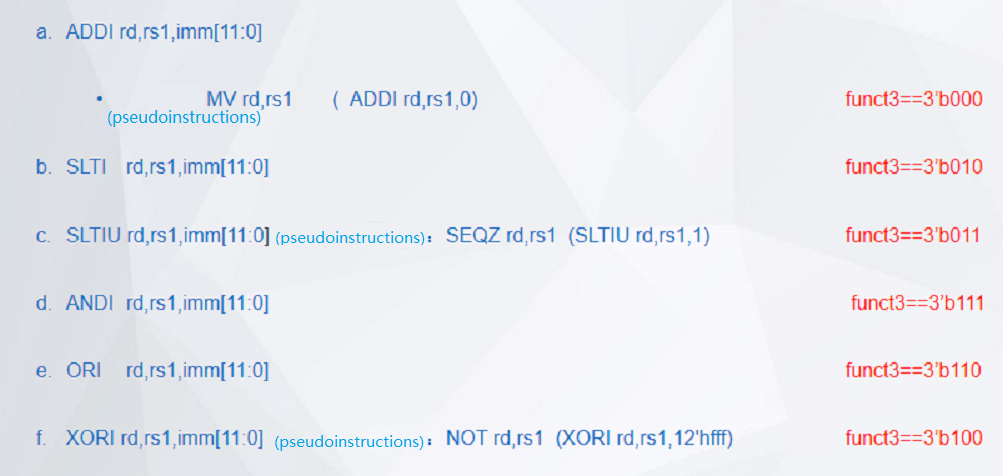
Risc-V Bus and PipeLine – FII Risc-V Bus and Pipeline Design – Risc-V Tutorial and Exercise
V1.0
Fraser Innovation inc
RISCV FII-PRX100 (ARTIX-7, XC7A100T) XILINX FPGA Board Bus and Pipeline
Version Control
| Version | Date | Description |
| 1.0 | 10/28/2020 | Initial Release |
Copyright Notice:
© 2020 Fraser Innovation Inc ALL RIGHTS RESERVED
Without written permission of Fraser Innovation Inc, no unit or individual may extract or modify part of or all the contents of this manual. Offenders will be held liable for their legal responsibility.
Thank you for purchasing the FPGA development board. Please read the manual carefully before using the product and make sure that you know how to use the product correctly. Improper operation may damage the development board. This manual is constantly updated, and it is recommended that you download the latest version when using.
Official Shopping Website:
https://fpgamarketing.com/FII-PRX100-D-ARTIX-100T-XC7A100T-RISC-V-FPGA-Board-PRX100-D-1.htm
Content
1. Introduction to Bus 4
2. FII-RISCV Bus Design 9
3. Introduction to Pipeline 23
4. FII-RISCV Pipeline Design 31
5. Exercise 39
6. References 40
Introduction to Bus
In computing, a bus (originally from Latin word, omnibus) is a communication system that transfers data between components inside a computer, or between computers [1]. It is usually a transmission wire harness composed of wires. According to the types of information transmitted by the computer, the computer bus can be divided into data bus, address bus, and control bus, respectively used to transmit data, address and control signals.
There are some bus classification. For example, based on the bus’s primary role, connecting devices internally or externally, there are internal buses and external buses. SPI and I2C are internal buses, while Firewire (IEEE 1394) and GPIB (IEEE-488) are external buses. Also, the classification could be based on the data transmission form, buses could be either serial or parallel. Serial buses carry data word in parallel on multiple wires, and serial buses carry data in bit-serial form. For instance, PCIE and USB are serial buses, while ISA and wishbone are parallel.
The reason why using buses is to standardize the data format of both input and output, so that the data communication between CPU and peripherals, peripherals and peripherals does not depend on its own data format. Since there are huge amount of different peripherals, so as the data format of peripherals, it is vital to adopt on the same standard. When the computer accesses multiple peripherals, like printers, microphones, keyboards, as long as the computer is using the USB protocol, and cooperate with the corresponding software, the peripherals can work without designing varies of interfaces connecting with the computer. In this way, the design of different interfaces has been eliminated, and the design of the computer and the peripherals are separated and simplified.
RAM, FIFO, FLASH and etc. are all FPGA’s internal logic, but they have different modules and communication interfaces. Below are the interface modules of RAM and FIFO.
//RAM module
//single port RAM, could be dual_port
TSP_RAM your_instance_name
(
.clka (clka), // input wire clka
.wea (wea), // input wire [0 : 0] wea
.addra (addra), // input wire [11 : 0] addra
//the second time to instantiate RAM, may require a different length of address
.dina (dina), // input wire [31 : 0] dina
.douta (douta), // output wire [31 : 0] douta
);
//FIFO module
fifo_generator your_instance_name (
.clk (clk), // input wire clk
.srst (srst), // input wire srst, reset
.din (din), // input wire [7 : 0] din
.wr_en (wr_en), // input wire wr_en
.rd_en (rd_en), // input wire rd_en
.dout (dout), // output wire [7 : 0] dout
//FIFO full/empty
.full (full), // output wire full
.empty (empty) // output wire empty
);
CPU needs to connect both RAM and FIFO, while it is obvious that they have different data length, and different address format. If CPU does not need to design every specific interface with each, a lot of time saved for designing CPU itself, instead of designing the connection with peripherals. Here is an example of RISCV CPU load and store module:
i_D_PC, //peripherals address (like FIFO, RAM)
i_LOAD, //load instruction
i_load_instr, // {rv32i_lbu,rv32i_lb,rv32i_lhu,rv32i_lh,rv32i_lw};
o_rd_wen, //read, write enable
i_rd_idx, //register index, used to write back
o_wb_data, //write back data
i_STORE, //store instruction
i_store_instr, // {rv32i_sb,rv32i_sh,rv32i_sw};
i_rs2_val, //actual value stored on the peripherals
It can be seen that CPU interface is also different from the peripherals. Furthermore, the peripherals are always developing. Without bus, even the CPU is considering every peripherals when it is initially designed, with the expansion of peripherals, it will eventually cause trouble.
Assume there is no bus between CPU and peripherals, then some issues need to be resolved.
- Convert the instruction information decoded by the CPU into the signal required by the RAM interface. And convert the instruction information decoded by the CPU into the signal required by the FIFO interface
- Clock mismatch. The peripheral may be a super low-speed device, or a device that can get data in multiple clock cycles (e.g. DDR needs tens of clocks to read or write data one time)
- RISCV CPU designers have to deal with different peripherals one by one. In this way, CPU core designers and peripheral IP designers must cooperate.
- Many projects are completed by multiple developers or multiple companies, which increase service communication costs.
The solution is to use bus. The benefits are as follows:
- With the same standard, no need to care about the peripheral interfaces
- No need to care about the clock mismatch between the CPU and peripherals
- The CPU designer concentrates on designing the CPU core. Peripheral developers pay attention to related development of peripherals. Everyone abides by the bus specification and can easily achieve interconnection.
- Bus can be expanded and interconnected.
- For example, FII-RISCV bus can be expanded as AHB, while the current bus structure will not be destroyed, and the IP core previously connected by AHB can be used directly.
- It is very helpful tailoring the peripheral as well. CPU does not need to change, only the address is updated, and the chip is tailored.
In all, bus is necessary as an agreement standard, and is a solution from practice.
FII-RISCV Bus Design
FII-RISCV bus design is shown in the following code block. The detailed explanation is commended inside the code block.
//FII-RISCV bus design:RIB (RISCV internal bus)
output [31:0] o_rib_maddr, // address bus
output [31:0] o_rib_mdout, // data bus
input [31:0] i_rib_mdin, //data bus
output o_rib_mvalid, // control bus
input [1:0] i_rib_mready, // control bus
output [3:0] o_rib_mwe, // control bus
output o_rib_mrd, // control bus
output o_rib_mop, // control bus
//FII-RISCV master bus design (cpu):
output [31:0] o_rib_maddr, // master transmit, 32-bit address
output [31:0] o_rib_mdout, // master transmit, 32-bit data (write operation)
input [31:0] i_rib_mdin, // master receive, 32-bit data (read operation)
output o_rib_mvalid, // master transmit, indicate operation (read/write) occurs
input [1:0] i_rib_mready, // master receive, bit[1] = bus error, bit[0] = peripherals ready
output [3:0] o_rib_mwe, // master transmit, write operation signal, each bit represents one operation (single edge)
output o_rib_mrd, // master transmit, read operation signal (single edge)
output o_rib_mop, // master transmit, indicate every operation (single edge)
//FII-RISCV slave bus design (peripherals):
input [31:0] i_rib_saddr, // slave receive, 32-bit address
input [31:0] i_rib_sdin, // slave receive, 32-bit data (write operation)
output [31:0] o_rib_sdout, // slave transmit, 32-bit data (read operation)
input i_rib_svalid, // slave receive, indicate operation (read/write) occurs
output [1:0] o_rib_sready, // slave transmit, bit[1] = bus error, bit[0] = peripherals ready
input [3:0] i_rib_swe, // slave receive, write operation signal, each bit represents one operation (single edge)
input i_rib_srd, // slave receive, read operation (single edge)
input i_rib_sop, // slave receive, indicate every operation (single edge)
Next, separate read and write operations for analyzing, the simplest single clock cycle bus read operation timing diagram is shown in Figure 1. Note that:
- mvalid, mready[0] set high simultaneously
- read signal, address, read data, mop (operation signal) are all single clock cycle operations
In the figure, the gray waveform means invalid area (do not care). Blue waveform means output (for CPU), green waveform is the input (for CPU).
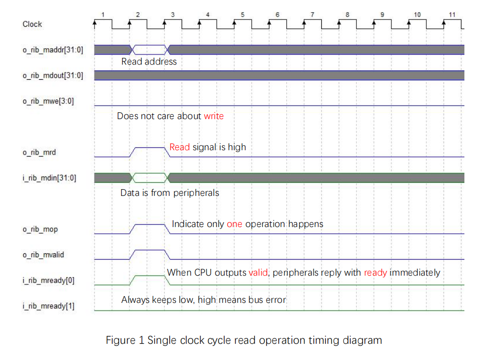
Figure 1 Single clock cycle read operation timing diagram
The numerical example is as follows: for address 32’h9000_00xx, read data (mdin) 32’h1234_5678.
mrd = 1, 32’hxxxx_xx78, maddr = 32’h9000_0000 lb(u)
mrd = 1, 32’hxxxx_56xx maddr = 32’h9000_0001 lb(u)
mrd = 1, 32’hxx34_xxxx maddr = 32’h9000_0002 lb(u)
mrd = 1, 32’h12xx_xxxx maddr = 32’h9000_0003 lb(u)
mrd = 1, 32’hxxxx_5678 maddr = 32’h9000_0000 lh(u)
mrd = 1, 32’h1234_xxxx maddr = 32’h9000_0002 lh(u)
mrd = 1, 32’h1234_5678 maddr = 32’h9000_0000 lw
The single clock cycle bus write operation timing diagram is shown in Figure 2. Note that similar to the single clock cycle bus read operation:
- mvalid, mready[0] set high simultaneously
- write signal, address, write data, mop (operation signal) are all single clock cycle operations
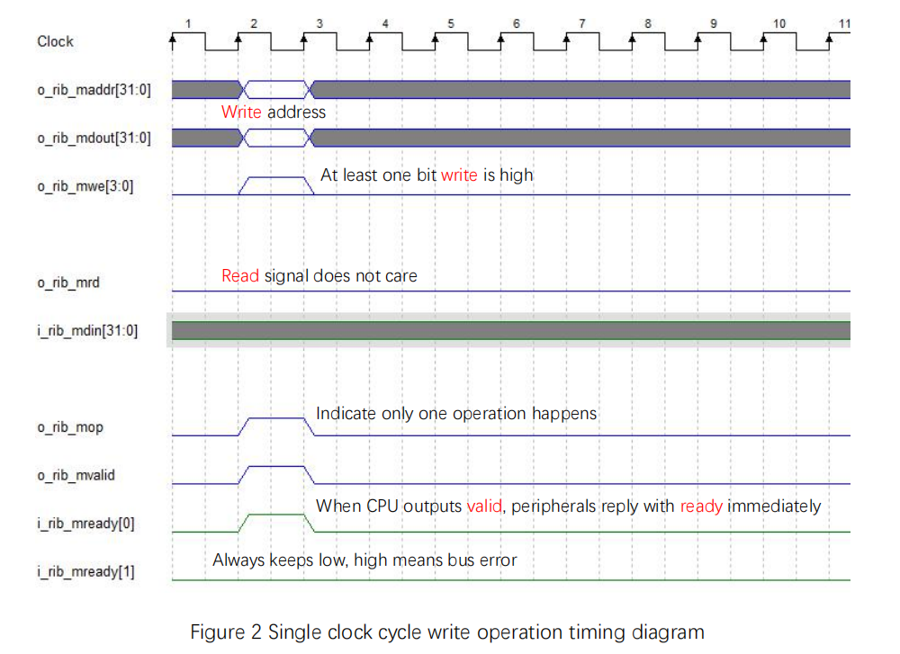
Figure 2 Single clock cycle write operation timing diagram
Similar to the numerical read example, the write numerical example is as follows: for address 32’h9000_00xx, write data (mdout) 32’h1234_5678.
mwe = 4’b0001, 32’hxxxx_xx78, maddr= 32’h9000_0000 sb
mwe = 4’b0010, 32’hxxxx_56xx maddr= 32’h9000_0001 sb
mwe = 4’b0100, 32’hxx34_xxxx maddr= 32’h9000_0002 sb
mwe = 4’b1000, 32’h12xx_xxxx maddr= 32’h9000_0003 sb
mwe = 4’b0011, 32’hxxxx_5678 maddr= 32’h9000_0000 sh
mwe = 4’b1100, 32’h1234_xxxx maddr= 32’h9000_0002 sh
mwe = 4’b1111, 32’h1234_5678 maddr= 32’h9000_0000 sw
Now elevate to single clock cycle read continuously operation, the timing diagram is shown in Figure 3. Same with the single clock cycle read operation:
- mvalid, mready[0] set high simultaneously
- read signal, address, read data, mop (operation signal) are all single clock cycle operations
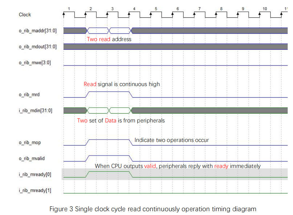
Figure 3 Single clock cycle read continuously operation timing diagram
Single clock cycle write continuously operation timing diagram is shown in Figure 4:
- mvalid, mready[0] set high simultaneously
- write signal, address, write data, mop (operation signal) are all single clock cycle operations
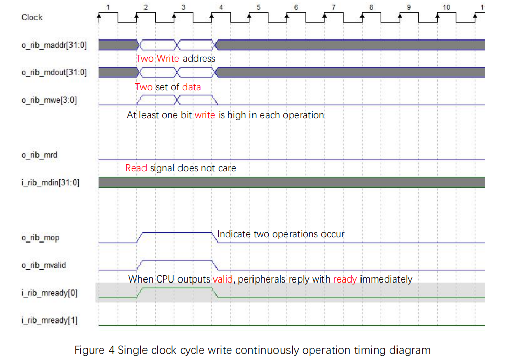
Figure 4 Single clock cycle write continuously operation timing diagram
Multiple clock cycles bus read operation timing diagram is shown in Figure 5. Multiple cycles means that ready is not responding valid immediately, such as the peripheral is in slow pace.
- With mvaild is high, only after the data is prepared, mready[0] is set high
- read signal and address are multiple clock cycle operations, read data and mop are single clock cycle operations
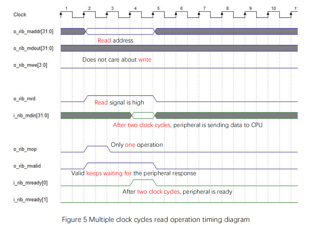
Figure 5 Multiple clock cycles read operation timing diagram
Multiple clock cycles bus write operation timing diagram is shown in Figure 6.
- With mvaild is high, only after the data is prepared, mready[0] is set high
- write signal, address, and write data are all multiple clock cycle operations. mop is single clock cycle operations
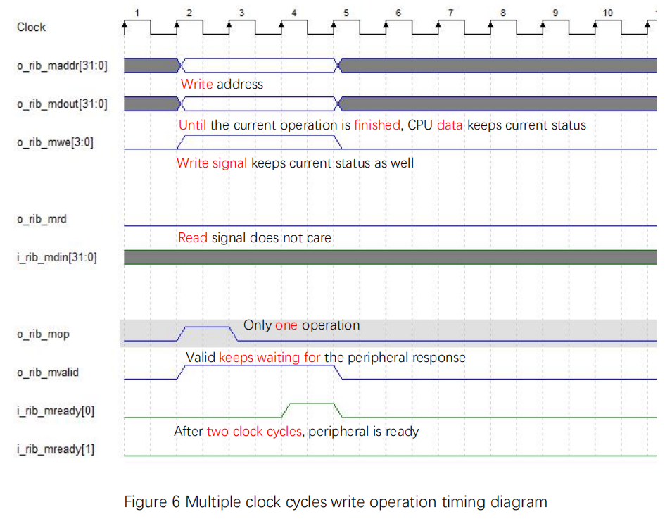
Figure 6 Multiple clock cycles write operation timing diagram
Multiple clock cycles bus read continuously operation timing diagram is shown in Figure 7.
- With mvaild is high, only after the data is prepared, mready[0] is set high
- read signal and address are multiple clock cycle operations. read data and mop are single clock cycle operations
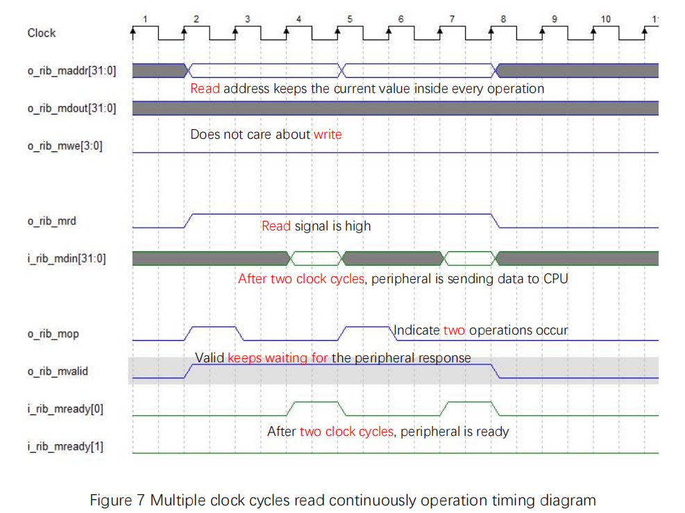
Figure 7 Multiple clock cycles read continuously operation timing diagram
Multiple clock cycles bus write continuously operation timing diagram is shown in Figure 8.
- With mvaild is high, only after the data is prepared, mready[0] is set high
- write signal, address and write data are all multiple clock cycle operations. mop is single clock cycle operation
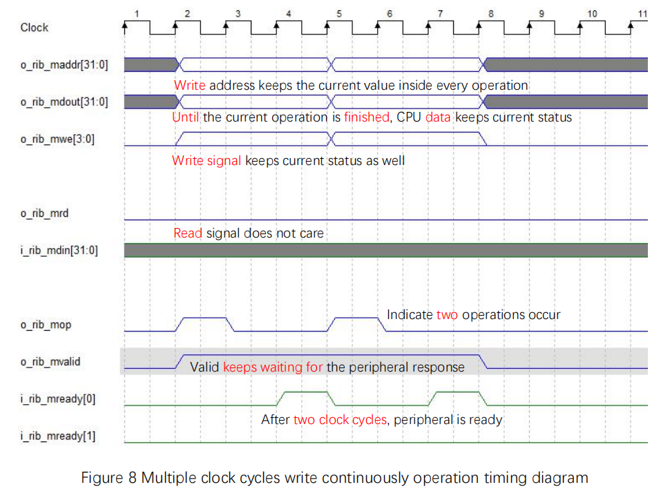
Figure 8 Multiple clock cycles write continuously operation timing diagram
The corresponding code block is shown below. The detailed explanation is commended inside the code block.
localparam DEV_NUM = 10;
wire [DEV_NUM – 1:0] s_cs;//slave chip select
assign s_cs[0] = ( i_rib_maddr[31:12] == DBG_BASEADDR[31:12] ) ? 1’b1 : 1’b0;//jtag debug
assign s_cs[1] = ( i_rib_maddr[31:16] == PLIC_BASEADDR[31:16] ) ? 1’b1 : 1’b0;//external interrupt
assign s_cs[2] = ( i_rib_maddr[31:16] == CPU_BASEADDR[31:16] ) ? 1’b1 : 1’b0;//CPU
assign s_cs[3] = ( i_rib_maddr[31:16] == MEM_BASEADDR[31:16] ) ? 1’b1 : 1’b0;//memory block
assign s_cs[4] = ( i_rib_maddr[31:16] == TMR_BASEADDR[31:16] ) ? 1’b1 : 1’b0;//timer interrupt
assign s_cs[5] = ( i_rib_maddr[31:16] == GPIO_BASEADDR[31:16] ) ? 1’b1 : 1’b0;//GPIO
assign s_cs[6] = ( i_rib_maddr[31:16] == UART_BASEADDR[31:16] ) ? 1’b1 : 1’b0;//UART
//some unused selection, could be expanded later
assign s_cs[7] = 1’b0;
assign s_cs[8] = 1’b0;
assign s_cs[9] = 1’b0;
//===============================================================================
always @ ( * )
if(!rst_n)
begin
o_rib_saddr = 0;
o_rib_sdin = 0;
o_rib_svalid = 0;
o_rib_swe = 0;
o_rib_srd = 0;
o_rib_sop = 0;
end
else
begin
//information transmitted by the master, every peripheral can receive it (function as broadcast)
o_rib_saddr = i_rib_maddr;
o_rib_sdin = i_rib_mdout;
o_rib_svalid = i_rib_mvalid;
o_rib_swe = i_rib_mwe;
o_rib_srd = i_rib_mrd;
o_rib_sop = i_rib_mop;
end
//===============================================================================
wire bus_err_ack = (i_rib_maddr == i_PC) ? 1’b1 : 1’b0;
always @ ( * )
begin
//the information transmitted by peripherals cannot be the same time
//if the current chip selection is high, the corresponding peripheral will return data and ready
//together with master information transmit, it is a bus splitter/multiplexer
case (s_cs)
10’b00_0000_0001: // DBG_BASEADDR
begin
o_rib_mdin = i0_rib_sdout;
o_rib_mready = i0_rib_sready;
end
10’b00_0000_0010: // PLIC_BASEADDR
begin
o_rib_mdin = i1_rib_sdout;
o_rib_mready = i1_rib_sready;
end
10’b00_0000_0100: // CPU_BASEADDR
begin
o_rib_mdin = i2_rib_sdout;
o_rib_mready = i2_rib_sready;
end
10’b00_0000_1000: // MEM_BASEADDR
begin
o_rib_mdin = i3_rib_sdout;
o_rib_mready = i3_rib_sready;
end
10’b00_0001_0000: // TMR_BASEADDR
begin
o_rib_mdin = i4_rib_sdout;
o_rib_mready = i4_rib_sready;
end
10’b00_0010_0000: // GPIO_BASEADDR
begin
o_rib_mdin = i5_rib_sdout;
o_rib_mready = i5_rib_sready;
end
10’b00_0100_0000: // UART_BASEADDR
begin
o_rib_mdin = i6_rib_sdout;
o_rib_mready = i6_rib_sready;
end
10’b00_1000_0000:
begin
o_rib_mdin = i7_rib_sdout;
o_rib_mready = i7_rib_sready;
end
10’b01_0000_0000:
begin
o_rib_mdin = i8_rib_sdout;
o_rib_mready = i8_rib_sready;
end
10’b10_0000_0000:
begin
o_rib_mdin = i9_rib_sdout;
o_rib_mready = i9_rib_sready;
end
default:
begin
o_rib_mdin = 0;
o_rib_mready = {1’b1, bus_err_ack};
end
endcase
end
Introduction to Pipeline
Before introducing pipeline, the finite-state machine (FSM, or just state machine) should be referred. The state machine CPU has a set of states, and a transition function to map input symbols and current states to a next one [2]. Every time CPU only executes one state, then loop repeat.
FII-RISCV has a state machine version, the code block is shown as follows, and the detailed explanation is commended inside the code block.
`DBG_INFO reg [ 2: 0 ] instr_st = 0;
reg [ 2: 0 ] instr_st_nxt = 0;
always@( posedge sys_clk )
if (( rst_n == 1’b0 ) | i_cpu_reset ) instr_st <= IDLE;
else instr_st <= instr_st_nxt;
always @ ( * )
begin
case ( instr_st )
//IDLE is when the FPGA board is in power-on reset state
//the normal execution states are fetch, execution, and write back.
//every clock cycle only executes one state. The one complete loop costs at least 3 clock cycles
//if with long period instructions, the execution time will be longer
IDLE: // 0
begin
if(!i_cpu_reset)
instr_st_nxt = I_FCH;
else
instr_st_nxt = IDLE;
end
I_FCH: // 1
begin
if(i_cpu_reset) instr_st_nxt = IDLE;
else instr_st_nxt = I_EXE;
end
I_EXE: // 2
begin
if ( i_ls_need )
begin
if ( ls_rib_ok )
instr_st_nxt = I_WB;
else
instr_st_nxt = I_EXE;
end
else
instr_st_nxt = I_WB;
end
I_WB: // 3
begin
instr_st_nxt = I_FCH;
end
default : instr_st_nxt = IDLE;
endcase
end
There is an example assembly file shown in Figure 9.
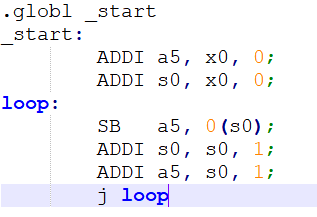
Figure 9 assembly file

Figure 10 State machine states in clock cycles
Numbers in Figure 10 means clock cycle, different instruction states are drawn in different colors. It simply shows that for state machine CPU:
- 1 clock: FCH, fetch the instruction, ADDI
- 2 clock: EXE, execute ADDI
- 3 clock: WB, write the result of X0 + 0 to a5
- 4 clock: FCH, fetch the instruction, ADDI
- 5 clock: EXE, execute ADDI
- 6 clock: WB, write the result of X0 + 0 to s0
- …
For the same sample assembly code, the pipeline is executing differently. See Figure 11 for details. Here is an example of 3-stage pipeline.
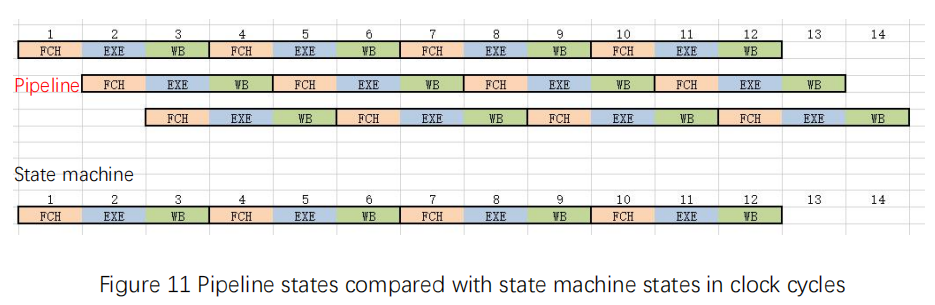
Figure 11 Pipeline states compared with state machine states in clock cycles
For pipeline:
- 1 clock: FCH, fetch the instruction, ADDI
- 2 clock: EXE&FCH, execute ADDI & fetch the instruction ADDI
- 3 clock: WB&EXE&FCH, write the result of X0 + 0 to a5 & execute ADDI & fetch the instruction SB
- 4 clock: FCH&WB&EXE, fetch the instruction ADDI & write the result of X0 +0 to s0 & execute SB
- …
Although for every single instruction, like 2 ADDI and SB, they still need 3 clock cycles each to finish, but under the same clock cycle, 3 instructions are executed in the same time. Except the first and second clock cycles, the pipeline is not fully filled, thus the execution efficiency is not high, the other clock cycles are all executing three instructions simultaneously. For the same period from 1 clock cycle to 12 clock cycles, the state machines executes 4 instructions, while the pipeline executes at least 10 instructions. When the clock speed is the same, pipelined CPU has absolutely higher efficiency than state machine CPU.
Pipeline in computing is also known as data pipeline. It is to decompose a repetitive process into several sub-processes, and each sub-process runs in parallel with other sub-process. Because this working method is very similar to the production pipeline in the factory, it is called pipeline technology, that is, in the same time, several sub-processes are executed together.
Classically, 5-stage pipeline includes fetch instruction, instruction decoder, execution, memory access, and writeback. FII-RISCV has combined instruction decoder and execution, memory access and writeback together to become 3-stage pipeline. Figure 12 shows FII-RISCV 3-stage pipeline. There are some classifications for pipelines. According to the execution order, pipeline could be divided to sequential pipeline and out-of-order pipeline. If the pipeline has feedback or feed-forward connection, then it is defined as non-linear pipeline. On the contrary, if the data in the pipeline flow from the first stage to the last stage, it is a linear pipeline. There are different stages of pipelines, up to 31 stages (hyper pipelined technology). The reason why different pipelined CPUs are developed and used is that under the same production process and the same clock, the efficiency of pipelined CPU instruction execution is largely improved, as well as the main frequency.
Figure 12 FII-RISCV 3-stage pipeline
Pipelined CPU has its price to pay for the high performance, such as it has more complicated logic than the state machine CPU. Also, there are mainly three types of hazard occurring along with pipelined CPU: data hazard, structural hazard, and control hazard.
- Data hazard
Data hazard occurs when instructions in different stages of a pipeline exhibit data dependence. For example in Figure 13, instruction 2 is depending on instruction 1, s0 is both the result of instruction1 and addend in instruction 2. While instruction 1 is writing the result back to the register, instruction 2 has executed using the wrong s0 value that is not updated. The solution is to bypass the value, which means specifically, s0 value in instruction 1 result will be passes to instruction 2 before writeback directly.
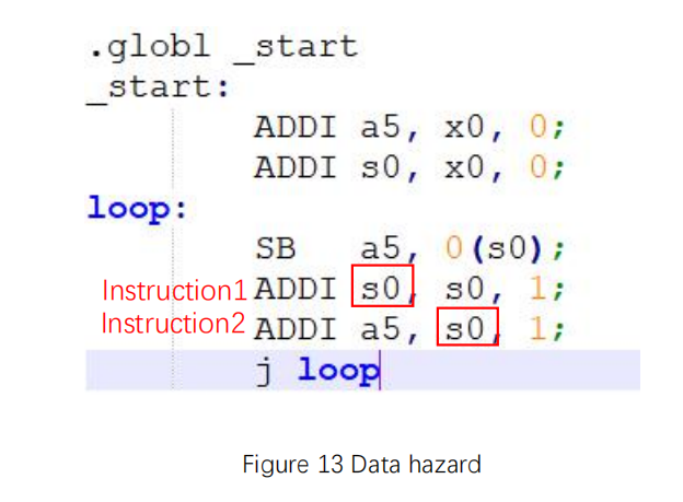
Figure 13 Data hazard
- Structural hazard
Structural hazard occurs when two or more instructions in the pipeline need the same resource. For example, when the instruction is fetched from the memory block and in the meantime, another instruction is writing back to the memory block. The solution is to add a pipeline bubble (nop) in front of the later instruction, or to increase available resources.
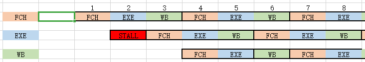
Figure 14 Structural hazard
- Control hazard
Control hazard occurs when the pipeline makes wrong decision on branch prediction, therefore the instruction that has been brought into the pipeline must be discarded. For example in Figure 15, when the j loop is being executed, the instruction following it has been fetched in the meantime. However, the PC (program counter) will jump to loop instead of pointing to the instruction that is already fetched. In this case, the pipeline will executed the already fetched instruction as nop (no operation).

Figure 15 Control hazard
FII-RISCV Pipeline Design
As mentioned before, FII-RISCV is 3-stage pipelined CPU. The three stages are:
- Fetch
Fetch the instructions from ITCM according to the PC.
- Execution
Execute the current instruction, including instruction decode and instruction execution.
- Writeback
Only when modifying 31 registers (register x0 which is hardwired to 0 is not counted) or read/write peripherals needs this stage. This stage could be skipped according to needs, thus saving one clock cycle. If it takes a long time for the peripheral to get the data, the pipeline will be suspended (PC is not changing, and the nop is sent).
According to the feedback in writeback stage, FII-RISCV is a non-linear pipeline.
As mentioned above for handling the pipeline data hazard, specifically in read after write situation. As shown in Figure 16, when the previous writeback register is the same as the next instruction fetch register, the value is directly bypassed.
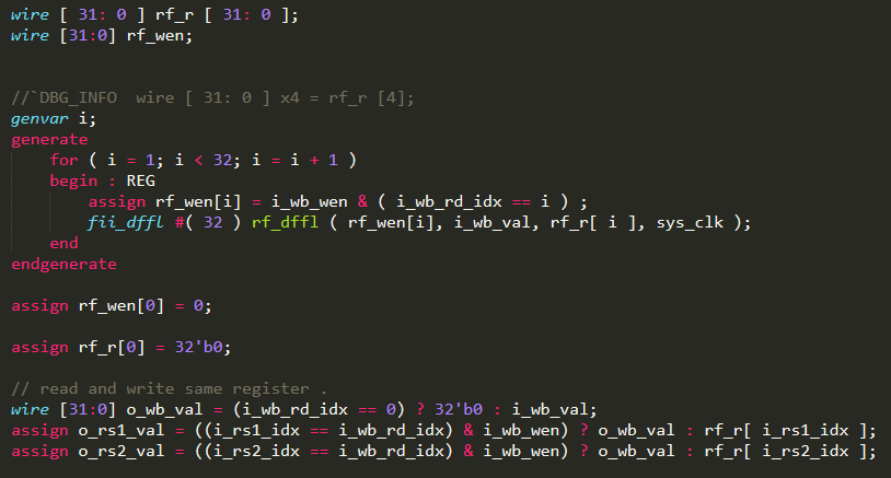
Figure 16 FPGA code in resolving data hazard
In the stage 1, assign the next instruction address to the instr_fch_pc, according to the situation. Normally, PC+4 is the next instruction address. When there is a jump related instruction or long period load and store, the PC will be assigned a different value to get the correct next instruction address, as shown in Figure 17. In the stage 2, output instr_fch_pc to the i_PC.
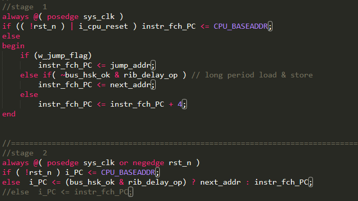
Figure 17 instr_fch_pc
Figure 18 lists the code for jump situations, and according to the jump type, assign different address to jump_addr. The jump flags are as follows:
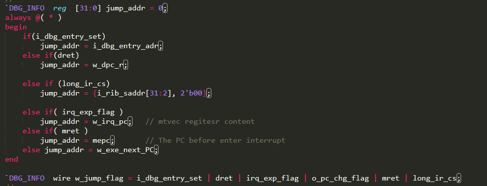
Figure 18 jump_addr and jump_flag
| Flag | Description | Flag | Description |
| I_dbg_entry_set | Jtag debugging mode | dret | Exit debug mode |
| Long_ir_cs | Long period instruction | Irq_exp_flag | Enter interrupt |
| mret | Exit interrupt | default | Jump instruction |
Table 1 Jump flags
Figure 19 shows assigning jump flags to the waiting_r. As long as any jump happens, waiting_r is pulled high. In Figure 20, `INST_NOP (no operation) is assigned to curr_instr if waiting_r is high. When jump instruction happen, the instruction after it which has been brought into pipeline already will be replaced with nop. `INST_NOP (0x0000_0001) is decoded as nop, which will not operate on memory or address.
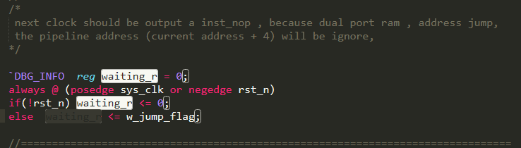
Figure 19 waiting_r

Figure 20 Assign curr_instr nop
Figure 21 shows a disassembly example which displays character “F” in segment display. It is obvious that before label <START>, every instruction is fetched, executed and wrote back by the pipeline in order. However, in 8000_003c, there is a branch condition. If it is satisfied, PC will jump to 8000_0038 instead of the 8000_0040 instruction. When the pipeline has already fetched 8000_0040 instruction, the execution of it should be handled with attention.
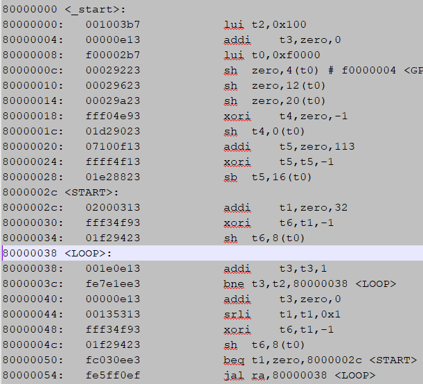
Figure 21 Jump example
The simulation result is shown in Figure 22. It can be seen that when curr_instr is 0x0000_0001, that is, the curr_instr has been assigned with nop, the i_PC will change from 0x8000_0040 to 0x8000_0038 with some delays. As mentioned before, jump flags will make the curr_instr change from whatever instruction to `INST_NOP.
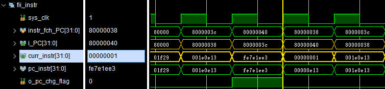
Figure 22 Simulation result
Figure 23 shows an another UART example. It will output “ This is a call function program” from UART. Figure 24 shows the information stored in rodata section. When the 0x8000_0044 instruction is being executed, 0x8000_0048 has been fetched already. However, the PC should point to 0x8000_0078 to load the print data according to the 0x8000_0044 instruction. At this time, the 0x8000_0048 instruction is abandoned, and the address is kept until the 0x8000_0078 rodata is loaded, PC will return pointing to 0x8000_0048. Figure 25 shows the simulation result of the UART example. It can be seen that curr_instr has been assigned to `INST_NOP (0x0000_0001) for the load instruction.
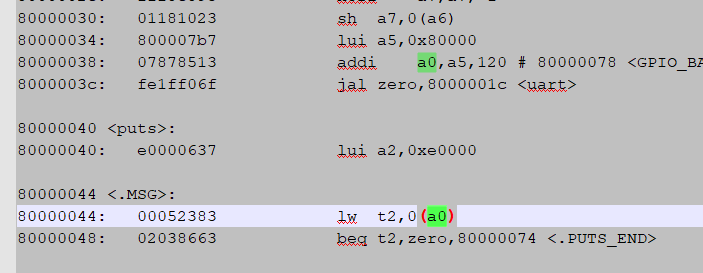
Figure 23 UART example
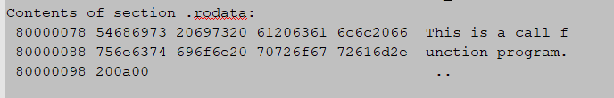
Figure 24 Print information
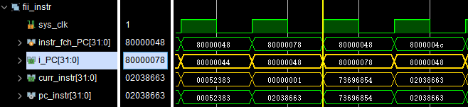
Figure 25 Simulation result
Before assigning the real address to the PC, assign the instr_fch_PC (PC+4) to the next_addr, since after the load/store has been executed, the normal PC+4 address will be the next executed PC, as shown in Figure 26. Figure 27 is the same as Figure 17, however, here rib_delay_op is highlighted. It is a decision making, if the current instruction is the long period load&store, assign next_addr to the instr_fch_PC, while the long period load&store is executed, assign the next_addr to the i_PC.
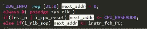
Figure 26 Assign the instr_fch_PC to next_addr

Figure 27 Long period load&store i_PC
Exercise
- Refer to RIB_FII_GPIO module or RIB_FII_UART module, create a new gpio group E (learn to use RIB bus), and add SW7-0 to the module. Write a C program to control LED by sliding the switches.
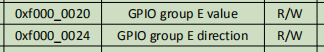
Figure 28 gpio group E address
References
- “Bus (computing) | Wikiwand”, Wikiwand, 2020. [Online]. Available: https://www.wikiwand.com/en/Bus_(computing). [Accessed: 05- Nov- 2020].
[2]Wiki.c2.com, 2020. [Online]. Available: https://wiki.c2.com/?FiniteStateMachine. [Accessed: 05- Nov- 2020].