Experimental Manuals FII-PRA040 FPGA Board Based FPGA Tutor Risc-V Risc-V Core

Frequency Division Design, Learn the BCD Code Counter, Digital Display Decoding Design, Segment Display – Altera Risc-V Board PRA040 Experimental 3

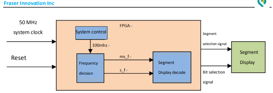
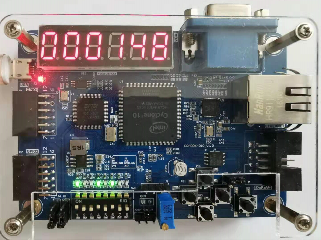
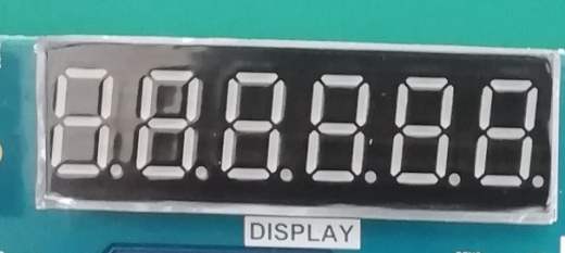
Experiment 3 Segment Display 3.1 Experiment Objective Review experiment 1, proficient in PLL configuration, frequency division design, and project verification; Learn the BCD code counter; Digital display decoding design; Learn to program the project into the serial FLASH of the development board; 3.2 Experiment Implement The segment display has two lower digits to display seconds, the middle two digits to display minutes, and the highest two digits to display hours. The decimal point remains off and will not be considered for the time being. 3.3 Experiment 3.3.1 Introduction to the…

Read More
Experimental Manuals FPGA Board Based FPGA for Beginners FPGA Tutor PRA006/PRA010

Use the BCD Code Counter, Digital Display Decoding Design, the Serial Flash, – Segment Display – FPGA Beginner Study Board PRA006, PRA010 Experiment 3

Experiment 3 Segment Display 3.1 Experiment Objective Review previous experiments, proficient practice in PLL configuration, frequency division design, and project verification; Learn to use the BCD code counter; Digital display decoding design; Learn to program the project into the serial FLASH of the development board; 3.2 Experiment Implement The segment display has two lower (right most) digits to display seconds, the middle two digits to display minutes, and the highest (left most) two digits to display hours. The decimal point remains off and will not be considered for the time…

Read More
Experimental Manuals FPGA Tutor Risc-V

AD,DA Experiment , write the data into PCF8591, Read the value of AD acquisition from PCF8591, – FII-PRA040 FPGA Board Experimental 12 – Altera Risc-V FPGA Tutorial :

Experiment 12 AD,DA Experiment 12.1 Experiment Objective Since in the real world, all naturally occurring signals are analog signals, and all that are read and processed in actual engineering are digital signals. There is a process of mutual conversion between natural and industrial signals (digital-to-analog conversion: DAC, analog-to-digital conversion: ADC). The purpose of this experiment is as follows: Learn about the theory of AD conversion Review the knowledge of the IIC protocol learned in the previous experiment and write the data into PCF8591 on the development board. Read the value…

Read More
Learn How to use ROM
FPGA Board Based FPGA for Beginners FPGA Tutor Pocket Boards PRA006/PRA010

Design 16 outputs ROM, Study the format of *.mif and how to edit *.mif file to configure the contents of ROM, Use of ROM (Read-only Memory) – FPGA Board for Beginner Tutorial – Experiment 8

Experiment 8 Use of ROM 8.1 Experiment Objective Study the internal memory block of FPGA Study the format of *.mif and how to edit *.mif file to configure the contents of ROM Learn to use RAM, read and write RAM 8.2 Experiment Implement Design 16 outputs ROM, address ranging 0-255 Interface 8-bit switch input as ROM’s address Segment display illustrates the contents of ROM and require conversion of hexadecimal to BCD output. 8.3 Experiment 8.3.1 Introduction to Program This experiment was carried out on the basis of Experiment 7, and…

Read More