Use Dual-port RAM to Read and Write Frame Data
Experimental Manuals FII-PE7030 FPGA Board Based FPGA Products FPGA Tutor

zynq xc7z030 board – FII-PE7030 Experiment 9 – Use Dual-port RAM to Read and Write Frame Data

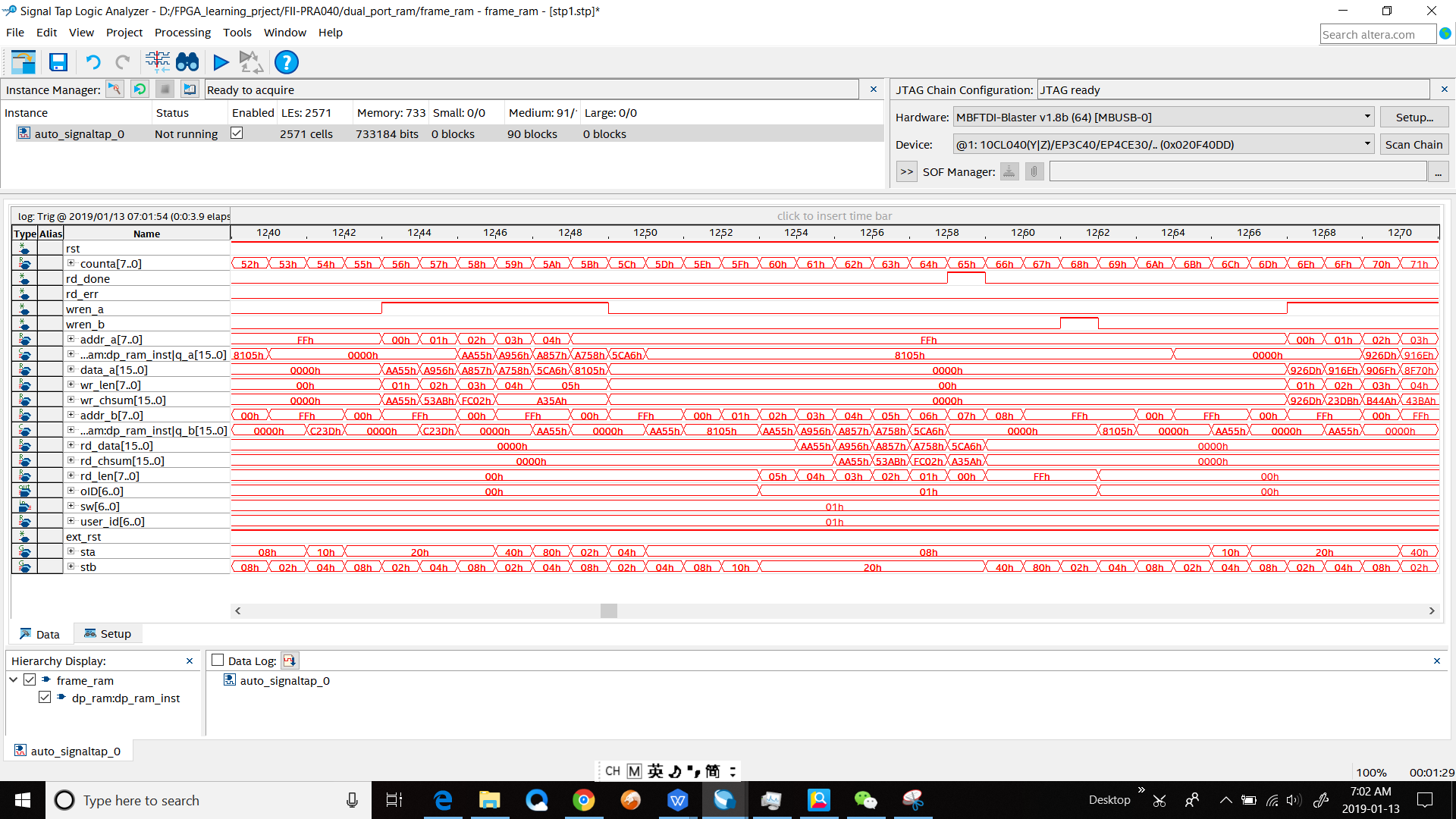
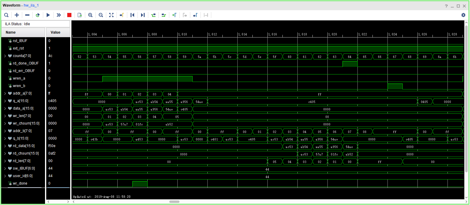
Experiment 9 Use Dual-port RAM to Read and Write Frame Data 9.1 Experiment Objective Learn to configure and use dual-port RAM Learn to use synchronous clock to control the synchronization of frame structure Learn to use asynchronous clock to control the synchronization of frame structure Use ILA to observe the structure of a synchronized clock frame Extended the use of dual-port RAM Design the use of three-stage state machine Experiment Implement Use ILA to observe the structure of a synchronized clock frame Extended the use of dual-port RAM Design the…

Read More
SignalTap II simulation
FPGA Board Based FPGA for Beginners FPGA Tutor Pocket Boards PRA006/PRA010

Use Dual-port RAM to Read and Write Frame Data, use synchronous (or asynchronous ) clock to control the synchronization of frame structure – FPGA Board Beginner Tutorial – Experiment 9

Experiment 9 Use Dual_port RAM to Read and Write Frame Data 9.1 Experiment Objective Learn to configure and use dual-port RAM Learn to use synchronous clock to control the synchronization of frame structure Learn to use asynchronous clock to control the synchronization of frame structure Experiment Implement Observing the synchronization structure of synchronous clock frames using SignalTap II Extended the use of dual-port RAM Design the use of three-stage state machine Design a 16-bit data frame Data is generated by an 8-bit counter: Data={~counta,counta} The ID of the data frame…

Read More
Learn How to use ROM
FPGA Board Based FPGA for Beginners FPGA Tutor Pocket Boards PRA006/PRA010

Design 16 outputs ROM, Study the format of *.mif and how to edit *.mif file to configure the contents of ROM, Use of ROM (Read-only Memory) – FPGA Board for Beginner Tutorial – Experiment 8

Experiment 8 Use of ROM 8.1 Experiment Objective Study the internal memory block of FPGA Study the format of *.mif and how to edit *.mif file to configure the contents of ROM Learn to use RAM, read and write RAM 8.2 Experiment Implement Design 16 outputs ROM, address ranging 0-255 Interface 8-bit switch input as ROM’s address Segment display illustrates the contents of ROM and require conversion of hexadecimal to BCD output. 8.3 Experiment 8.3.1 Introduction to Program This experiment was carried out on the basis of Experiment 7, and…

Read More