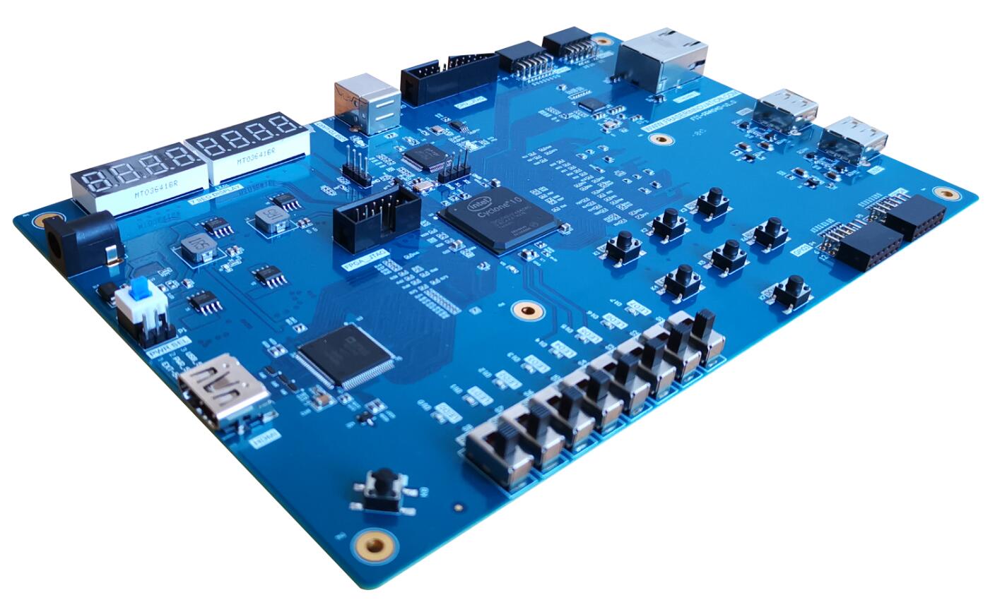
Audio 8978 Loopback Experiment – What is I2S (Inter-IC Sound) bus and how it works – AWM8978 Audio Boardudio – Xilinx Risc-V FII-PRX100 Board Experiment 16
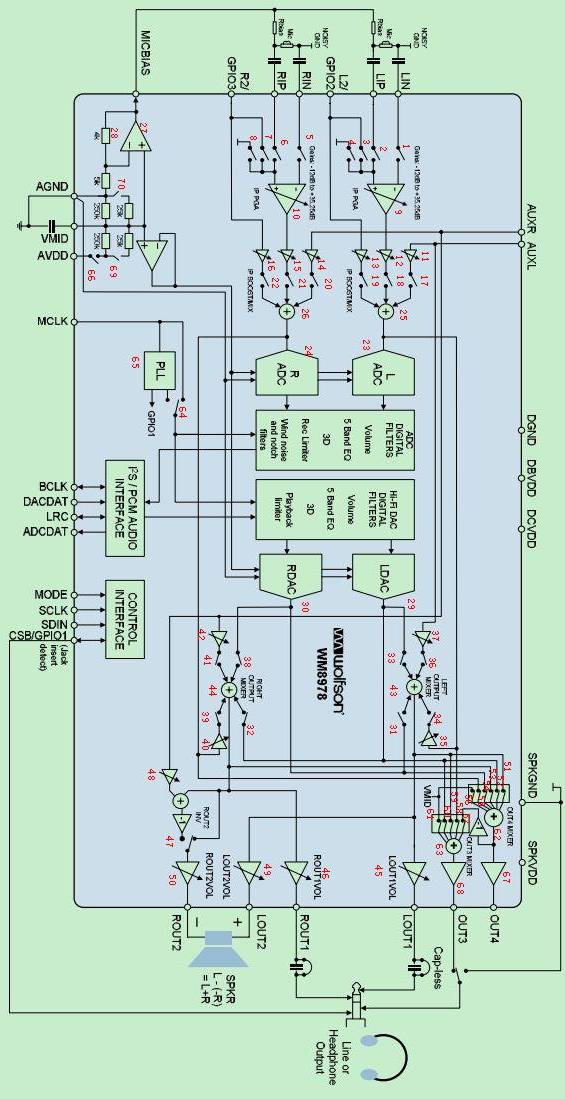
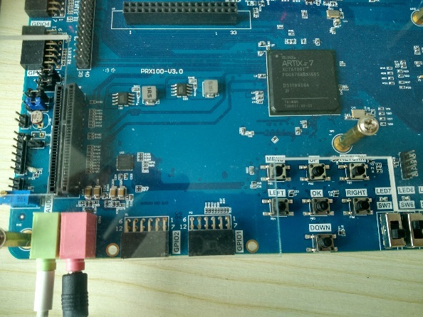
Experiment 16 8978 Audio Loopback Experiment 16.1 Experiment Objective Learn about I2S (Inter-IC Sound) bus and how it works Familiar with the working mode of WM8978. And by configuring the interface mode and selecting the relevant registers in combination with the development board, complete the data transmission and reception, and verify it 16.2 Experiment Implement Perform audio loopback test by configuring the onboard audio chip WM8978 to check if the hardware is working properly Adjust the volume output level with the push buttons. 16.3 Experiment 16.3.1 WM8978 Introduction WM8978 is…
Read More