SRAM read timing
Experimental Manuals FII-PRX100-S FII-PRX100D FPGA Board Based PRX100 Risc-V

Reading Experiment of Serial Port Partition of Static Memory SRAM, Read and write timing of IS61WV25616BLL SRAM, and prepare for the next experimental experiment of OV5640 camera experiment – – Xilinx Risc-V FII-PRX100 Board Experiment 17

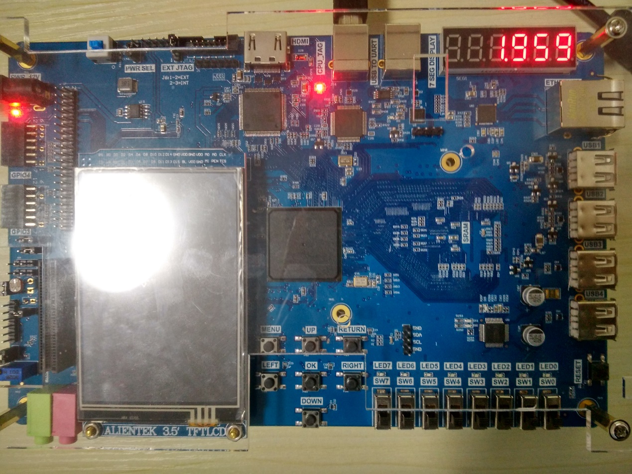
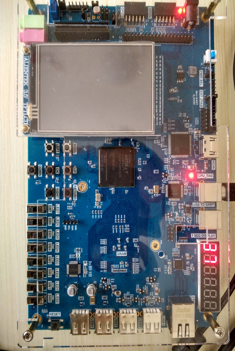
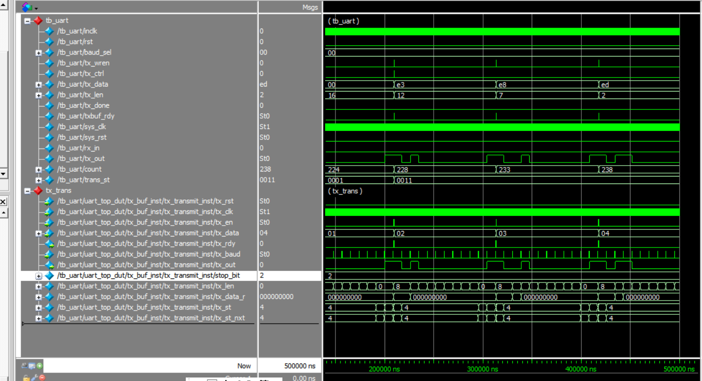
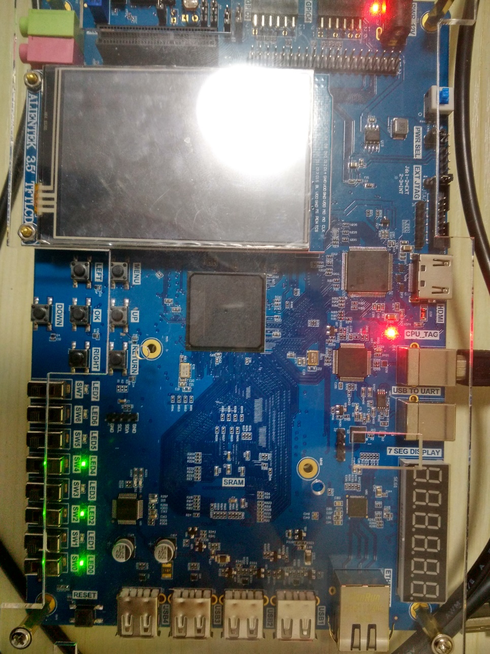
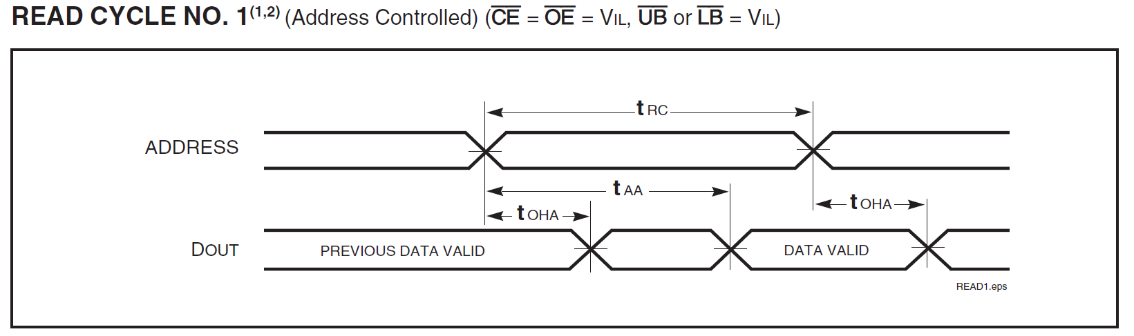
Experiment 17 Reading Experiment of Serial Port Partition of Static Memory SRAM 17.1 Experiment Objective Learn about static memory SRAM read and write operations and how it works Familiar with the read and write timing of IS61WV25616BLL SRAM, and prepare for the next experimental experiment of OV5640 camera experiment. 17.2 Experiment Implement The experimental board is equipped with two pieces of SRAM, which are combined to form 18-bit address lines and 32-bit data spaces. After power-on, the FPGA will write the same value in the corresponding address in the entire…

Read More
wm8978 board verification
FII-PRX100-S FII-PRX100D FPGA Board Based PRX100 Risc-V

Audio 8978 Loopback Experiment – What is I2S (Inter-IC Sound) bus and how it works – AWM8978 Audio Boardudio – Xilinx Risc-V FII-PRX100 Board Experiment 16

Experiment 16 8978 Audio Loopback Experiment 16.1 Experiment Objective Learn about I2S (Inter-IC Sound) bus and how it works Familiar with the working mode of WM8978. And by configuring the interface mode and selecting the relevant registers in combination with the development board, complete the data transmission and reception, and verify it 16.2 Experiment Implement Perform audio loopback test by configuring the onboard audio chip WM8978 to check if the hardware is working properly Adjust the volume output level with the push buttons. 16.3 Experiment 16.3.1 WM8978 Introduction WM8978 is…

Read More
Schematics of RTL8211E-VB
Experimental Manuals FII-PRX100-S FII-PRX100D FPGA Board Based FPGA Tutor PRX100 Risc-V

How ethernet work and familiar with MII, GMII, RGMII interface types – FII-PRX100 Risc-V Board Experiment 15

Experiment 15 Ethernet 15.1 Experiment Objective Understand what Ethernet is and how it works Familiar with the relationship between different interface types (MII, GMII, RGMII) and their advantages and disadvantages (FII-PRA040 uses RGMII) Combine the development board to complete the transmission and reception of data and verify it 15.2 Experiment Implement Perform a loopback test to check if the hardware is working properly. Perform data receiving verification Perform data transmission verification 15.3 Experiment 15.3.1 Introduction to Experiment Principle Ethernet is a baseband LAN technology. Ethernet communication is a communication method…

Read More
Signal waveform of AD9226 captured by logic analyzer
FII-PRX100-S FII-PRX100D PRX100

FII-PRX100T User Experiment Manuals (newly updated 2020-09-28)

  PRX100 USER experimental manual PRX100 EXPERIMENTAL INSTRUCTIONS FRASER INNOVATION INC December 11, 2019 Version Control Version Date Descrption V1.0 07/10/2019 Initial Release V1.1 09/16/2019 Modify part of pin assignments and Ethernet description V1.2 12/12/2019 Add Experiments 15-20 Contents: Part 1 FII-PRX100 Development System Introduction 6 1. System Design Objective 6 2. System Resource 6 3. Human-computer Interaction Interface 6 4. Software Development System 7 5. Supporting Resources 7 Part 2 FII-PRX100 Main Hardware Resources Usage and FPGA Development Experiment 7 Experiment 1 LED Shifting 7 1. Experiment Object 7…

Read More
Experimental Manuals FII-PRX100-S FII-PRX100D FPGA Products FPGA Tutor PRX100 Risc-V

RISC-V FPGA Board Study Guide – FII-PRX100 Experimental Manuals

Version Control Version Date Descrption V1.0 10/07/2019 Initial Release V1.1 16/09/2019 Modify part of pin assignments and Ethernet description Contents: Part 1 FII-PRX100 Development System Introduction 5 1. System Design Objective 5 2. System Resource 5 3. Human-computer Interaction Interface 5 4. Software Development System 6 5. Supporting Resources 6 Part 2 FII-PRX100 Main Hardware Resources Usage and FPGA Development Experiment 6 Experiment 1 LED Shifting 6 1. Experiment Object 6 2. Create A New Project Under Vivado 6 Experiment 2 Switches and display 25 1.Experiment Objective 25 2.Start New…

Read More
HDMI connection block diagram
Experimental Manuals FPGA Tutor PRX100 Risc-V

Understand the register configuration of the ADV7511, HDMI Graphic Display Experiment – Xilinx Risc-V Board Tutorial : FII-PRX100 FPGA Board Experiment 14

Experiment 14 HDMI Graphic Display Experiment 1.Experiment Objective Learn about video timing (2) Understand the register configuration of the ADV7511, reviewing the knowledge from experiment 12 2.Experiment Requirement Image display processing has always been the focus of FPGA research. At present, the image display mode is also developing. The image display interface is also gradually transitioning from the old VGA interface to the new DVI or HDMI interface. Display the image using the HDMI interface of the development board. Download the program to the board for comparison. Introduction to HDMI:…

Read More
AD, DA Experiment Results
Experimental Manuals FPGA Tutor PRX100 Risc-V

digital-to-analog conversion: DAC, analog-to-digital conversion: ADC – Xilinx Risc-V Board Tutorial : AD, DA Experiment – FII-PRX100 FPGA Board Experiment 13

Experiment 13 AD, DA Experiment 1.Experiment Objective Since in the real world, all naturally occurring signals are analog signals, and all that are read and processed in actual engineering are digital signals. There is a process of mutual conversion between natural and industrial signals (digital-to-analog conversion: DAC, analog-to-digital conversion: ADC). The purpose of this experiment is twofold: Learning the theory of AD conversion Read the value of AD acquisition from PCF8591, and convert the value obtained into actual value, display it with segment decoders 2.Experiment Requirement Perform analog-to-digital conversion using…

Read More
Demonstration of the develop board
Experimental Manuals FPGA Tutor PRX100 Risc-V

Learning the basic principles of the different IIC bus, mastering the IIC communication protocol, Xilinx Risc-V Board Tutorial : IIC Protocol Transmission – FII-PRX100 FPGA Board Experiment 12

Experiment 12 IIC Protocol Transmission 1.Experiment Objective There is an IIC interface EEPROM chip 24LC02 in the test plate, capacity sized 2 kbit (256 bite). Since the data is not lost after the EEPROM is powered down, users can store some hardware setup data or user information. Learning the basic principles of the different IIC bus, mastering the IIC communication protocol Master the method of reading and writing EEPROM Joint debugging using logic analyzer 2.Experiment Requirement Correctly write a number to any address in the EEPROM (this experiment writes to…

Read More
ModelSim simulation waves sent by serial
Experimental Manuals FPGA Tutor PRX100 Risc-V

Xilinx Risc-V Board Tutorial : Asynchronous Serial Port Design and Experiment – FII-PRX100 FPGA Board Experiment 11

Experiment 11 Asynchronous Serial Port Design and Experiment 1.Experiment Objective Because asynchronous serial ports are very common in industrial control, communication, and software debugging, they are also vital in FPGA development. Learning the basic principles of asynchronous serial port communication, handshake mechanism, data frame Master asynchronous sampling techniques Review the frame structure of the data packet Learning FIFO Joint debugging with common debugging software of PC (SSCOM, teraterm, etc.) 2.Experiment Requirement Design and transmit full-duplex asynchronous communication interface Tx, Rx Baud rate of 11520 bps, 8-bit data, 1 start bit,…

Read More
Risc-V Board - Dual_port RAM test result
Experimental Manuals FPGA Tutor PRX100 Risc-V

Xilinx Risc-V Board Tutorial : Use Dual_port RAM to Read and Write Frame Data – FII-PRX100 FPGA Board Experiment 10

Experiment 10 Use Dual_port RAM to Read and Write Frame Data 1.Experiment Objective Learn to configure and use dual-port RAM Learn to use synchronous clock to control the synchronization of frame structure Learn to use asynchronous clock to control the synchronization of frame structure Observing the synchronization structure of synchronous clock frames using ILA Extended the use of dual-port RAM Design the use of three-stage state machine 2.Experiment Requirement Generate dual-port RAM and PLL 16-bit width, 256-depth dual-port RAM 2 PLL, both 50 MHz input, different 100 MHz and 20…

Read More