Risc-V Use of ROM Results
Experimental Manuals FPGA Tutor PRX100 Risc-V

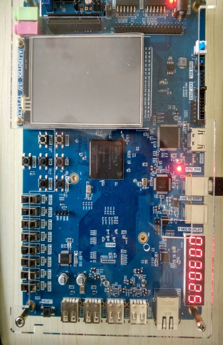
Study the internal memory block of FPGA, Study the format of *.mif and how to edit *.mif file to configure the contents of ROM : Use of ROM – FII-PRX100 Risc-V FPGA Board Experiment 9

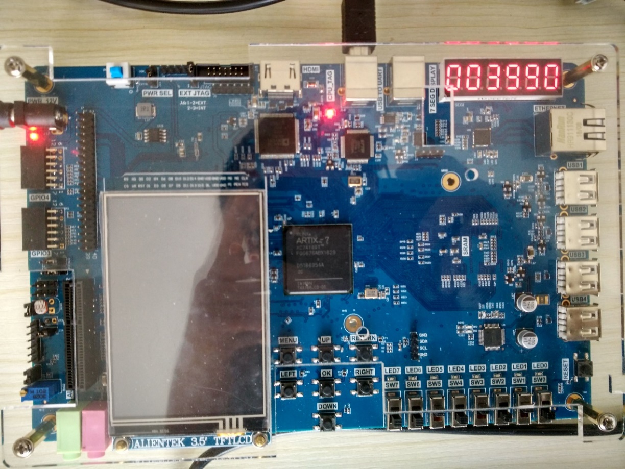
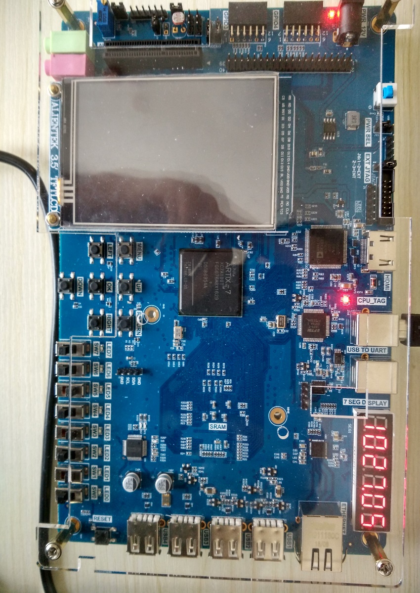
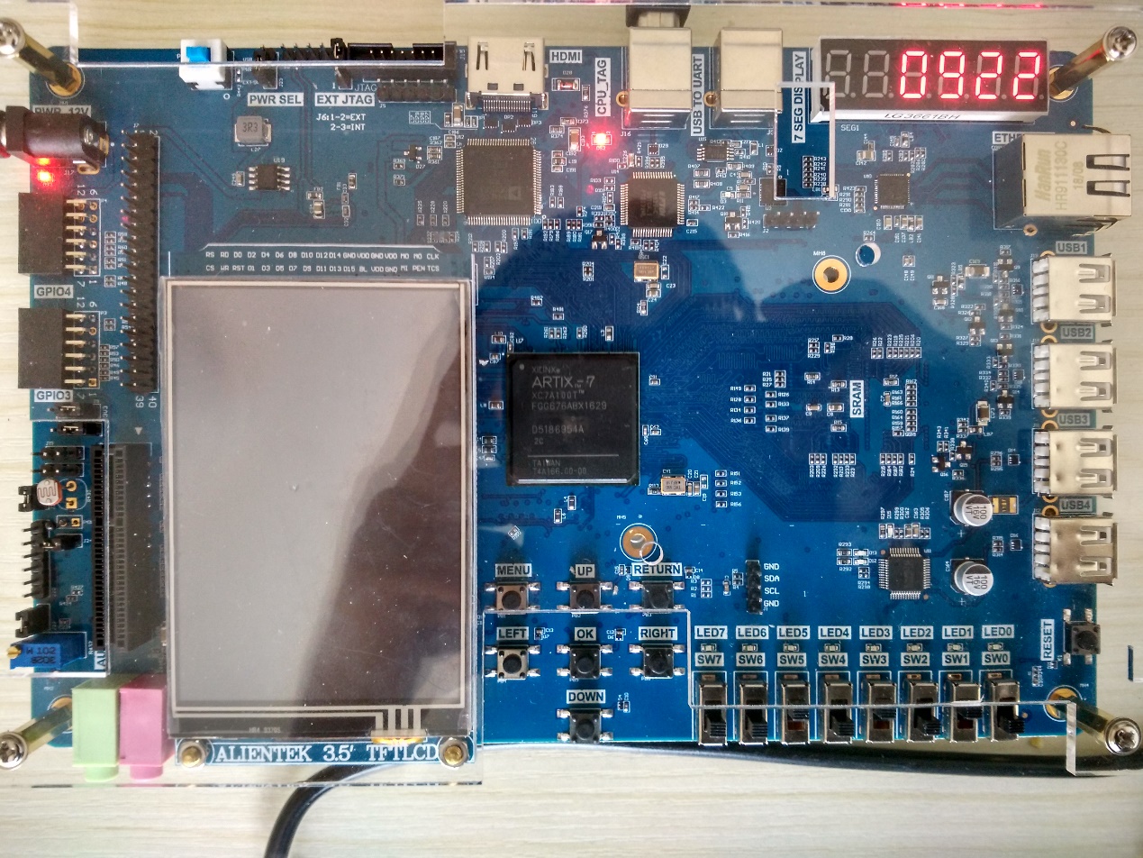
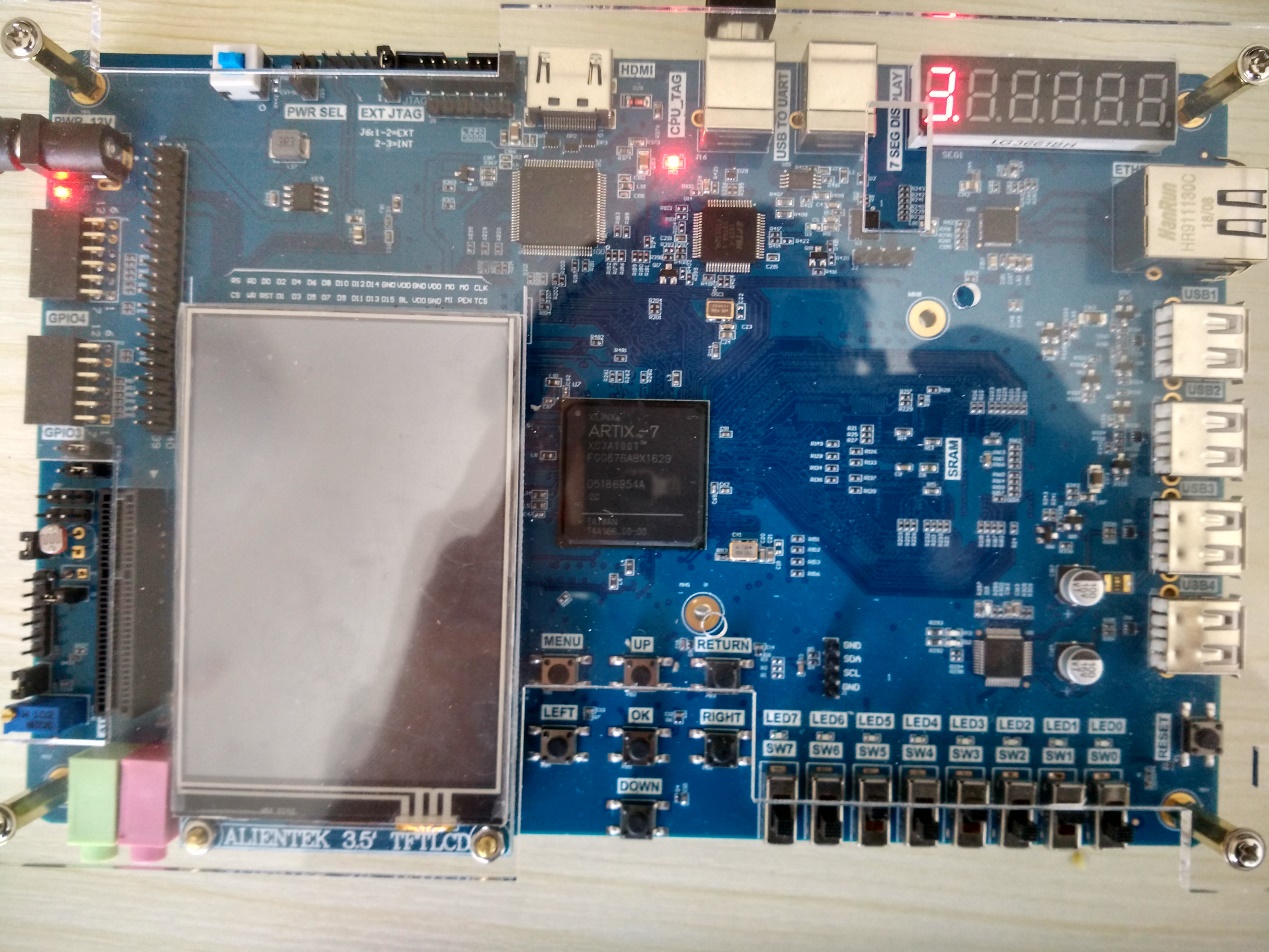
Experiment 9 Use of ROM 1.Experiment Objective Study the internal memory block of FPGA Study the format of *.mif and how to edit *.mif file to configure the contents of ROM Learn to use RAM, read and write RAM 2.Experiment Design Design 16 outputs ROM, address ranging 0-255 Interface 8-bit switch input as ROM’s address Segment decoders display the contents of ROM and require conversion of hexadecimal to BCD output. 3.Design Procedure Create a coe file. This experiment *.coe file is generated based on Matlab2018. The *.m file is as…

Read More
Risc-V Board
Experimental Manuals FPGA Tutor PRX100 Risc-V

Xilinx Risc-V Board Tutorial : Hexadecimal Number to BCD Code Conversion and Application – FII-PRX100 FPGA Board Experiment 8

Experiment 8 Hexadecimal Number to BCD Code Conversion and Application 1.Experiment Objective Since the hexadecimal display is not intuitive, decimal display is more widely used in real life. Human eye recognition is relatively slow, so the display from hexadecimal to decimal does not need to be too fast. Generally, there are two methods Countdown method: Under the control of the synchronous clock, the hexadecimal number is decremented by 1 until it is reduced to 0. At the same time, the appropriate BCD code decimal counter is designed to increment. When…

Read More
Risc-V Board Multiplier Use and ISIM Simulation
Experimental Manuals FPGA Tutor PRX100 Risc-V

Xilinx Risc-V Board Tutorial : Multiplier Use and ISIM Simulation- FII-PRX100 FPGA Board Experiment 7

Experiment 7 Multiplier Use and ISIM Simulation 1.Experiment Objective Learn to use multiplier Use ISIM to simulate design output 2.Experiment Design Build new project mult_sim Select device XC7A100TFGG676-2 Design requirement 8×8 multiplier, the first input value is an 8-bit switch, and the second input value is the output of an 8-bit counter. Observe the result on Modelsim Observe the result on 6 segment decoders Design procedure Create new file mult_sim.v  Add PLL,set the input clock to be 50 MHz, and the output clock to be 100 MHz Add LPM_MULT IP…

Read More
Risc-V Board - Digital Clock Comprehensive Design Experiment
Experimental Manuals FPGA Tutor PRX100 Risc-V

Xilinx Risc-V Board Tutorial : Digital Clock Comprehensive Design Experiment- FII-PRX100 FPGA Board Experiment 6

Experiment 6 Digital Clock Comprehensive Design Experiment 1.Experiment Objective Design month, day, hour, minute, and second digital clock experiments, using 6 segment decoders 60 seconds carried to the minute 60 minutes carried to the hour 24 hours carried to the day 30 days carried to the month, and reset all Set four keys: menu, left, up, down The menu key controls the calibration function to switch between clock, date, and alarm. The left key selects which value is currently calibrated The Up and down keys add 1 and subtract 1…

Read More
Button Debounce Design and Experimental-
Experimental Manuals FPGA Tutor PRX100 Risc-V

Xilinx Risc-V Board Tutorial : Button Debounce Design and Experimental- FII-PRX100 FPGA Board Experiment 5

Experiment 5 Button Debounce Design and Experimental 1.Experiment Objective Review the design of blinking LED Learn the principle of button debounce, and adaptive programming Learn the connection and use of the FII-PRX100T button schematics Integrated application of button debounce and another compatible program design 2.Experiment Button debounce principle Usually, the switches used for the buttons are mechanical elastic switches. When the mechanical contacts are opened and closed, due to the elastic action of the mechanical contacts, a push button switch does not immediately turn on when closed, nor is it…

Read More
Block/SCH Digital Clock Design
Experimental Manuals FPGA Tutor PRX100 Risc-V

Xilinx Risc-V Board Tutorial : Block/SCH Digital Clock Design- FII-PRX100 FPGA Board Experiment 4

Experiment 4 Block/SCH Digital Clock Design 1.Experiment Objective Review the new FPGA project building in Vivado, device selection, PLL creation, PLL frequency setting, Verilog tree hierarchy design, and the use of ILA Master the design method of graphics from top to bottom Combine the BCD_counter project to realize the movement of the decimal point (DP) of the decoder Observe the test result 2.Experiment Procedure File -> Project -> New Project Name:block_counter Select Device: XC7A100T-2FGG676I See Fig 4. 1, add source file, new top-level entity: block_counter.v Fig 4. 1 Build source…

Read More
isc-V Board Tutorial : Basic Digital Clock Experiment and Programming of FPGA Configuration Files
Experimental Manuals FPGA Tutor PRX100 Risc-V

Xilinx Risc-V Board Tutorial : Basic Digital Clock Experiment and Programming of FPGA Configuration Files- FII-PRX100 FPGA Board Experiment 3

Experiment 3 Basic Digital Clock Experiment and Programming of FPGA Configuration Files 1.Experiment Objective Review the contents of experiment 1 and experiment 2, master the configuration of PLL, the design of frequency divider, the principle of schematics and the pin assignment of FPGA. Study BCD decoder Display design of 4-digit hexadecimal to 7 segment display decoders Generate a programmable configuration file and program it to the serial FLASH of the development board through the JTAG interface. 2.Design of The Experiment Refer experiment 1 for building new projects, chip selection module…

Read More
Altera Risc-V fpga board
Experimental Manuals FPGA Tutor PRX100 Risc-V

Xilinx Risc-V Board Tutorial : Switches and Display – FII-PRX100 FPGA Board Experiment 2

Experiment 2 Switches and display 1.Experiment Objective Continue to practice using develop board Learn to use ILA (Integrated Logic Analyzer) in Vivado Learn to use the FPGA configuration memory for programming 2.Start New Project Refer to Experiment 1 Select the same chip in Experiment 1 Add PLL1 (Here PLL1 is optional, external input clock can be used directly) 3.Verilog HDL Code module SW_LED( input inclk, input [7:0] sw, output reg[7:0] led ); wire sys_clk; wire pll_locked; reg sys_rst; always@(posedge sys_clk) sys_rst<=!pll_locked;   always @(posedge inclk) if(sys_rst) led<=8’hff; else led<=~sw; PLL1…

Read More
Experimental Manuals FPGA Tutor PRX100 Risc-V

Verilog HDL program to achieve frequency division, Write Verilog HDL program to implement LED shifting – Risc-V FPGA Board Xilinx – Development Board Experiment 1 – LED Shifting – FII-PRX100

Experiment 1 LED Shifting 1. Experiment Object Practice how to use the development system software Vivado to establish a new project, call the system resource PLL to establish the clock. Write Verilog HDL program to achieve frequency division Write Verilog HDL program to implement LED shifting Combine hardware resources for FPGA pin configuration Compile Download the program to the develop board Observe the experimental result and debug the project 2. Create A New Project Under Vivado Start Vivado in the start Menu. See Fig 1. 1 Fig 1. 1 Start…

Read More
prx100 system block diagram
Experimental Manuals FPGA Tutor PRX100 Risc-V

xilinx Risc-V FPGA Board – FII-PRX100 – FPGA Development Board System Introduction

  FII-PRX100 Development Board ( ARTIX 100T, XC7A100T, RISC-V FPGA Developing Board) Online Shopping: https://fpgamarketing.com/FII-PRX100-ARTIX-100T-XC7A100T-RISC-V-FPGA-Board-PRX100-1.htm Fraser Innovation Inc develops FII-PRX100 based on the boards of the Xilinx ARTIX-7 series. It was initial released in 2018. This development board is resource-rich and high-speed, making it an ideal platform for learning and engineering research. This development board has been spent a lot on system design, PCB design, and function creation. It could even be said comprehensive and powerful. System Design Objective The main purpose of this system design is to complete FPGA learning,…

Read More