The knowledge of the IIC protocol, the Theory of AD Conversion, AD, DA Experiment – FPGA Beginner Study Board PRA006, PRA010 Experiment 12
Experiment 12 AD, DA Experiment
12.1 Experiment Objective
Since in the real world, all naturally occurring signals are analog signals, and all that are read and processed in actual engineering are digital signals. There is a process of mutual conversion between natural and industrial signals (digital-to-analog conversion: DAC, analog-to-digital conversion: ADC). The purpose of this experiment is as follows:
- Learn about the theory of AD conversion
- Review the knowledge of the IIC protocol learned in the previous experiment and write the data into PCF8591 on the development board.
- Read the value of AD acquisition from PCF8591, and convert the value obtained into actual value, display it with segment display
12.2 Experiment Implement
- The ADC port of the chip is used for analog-to-digital conversion. The chip is correctly configured. Three variable (potentiometer, photoresistor, thermistor) voltages on the development board are collected, and the collected voltage value is displayed through the segment display.
- Board downloading verification, compared with resistance characteristics, verify the correctness of the results
12.3 Experiment
Introduction to AD Conversion Chip PCF8591
The PCF8591 is a monolithically integrated, individually powered, low power consuming, 8-bit CMOS data acquisition device. The PCF8591 has four analog inputs, one analog output, and one serial IIC bus interface. The three address pins A0, A1 and A2 of the PCF8591 can be used for hardware address programming. The address, control signals and data signals of the input and output on the PCF8591 device are transmitted serially via the two-wire bidirectional IIC bus. Please refer to the previous experiment 11 for the contents of the IIC bus protocol. After the device address information and the read/write control word are sent, the control word information is sent.
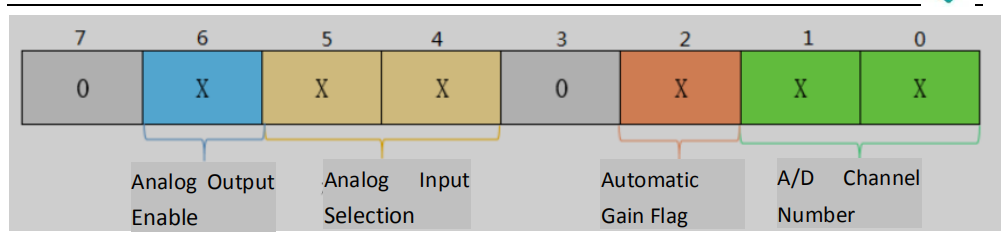
Figure 12.1 PCF8951 control word
The specific control word information is shown in Figure 12.1. Digit 1 – digit 0 is used for four channel settings, digit 2 is for automatic gain selection, ‘1’ is valid. Digit 5 – digit 4 determines analog input selection. Digit 6 is analog output enable. Digit 7 and digit 3 are reserved to be ‘0’. The second byte sent to PCF8951 is stored in the control register to control the device functionality. The upper nibble of the control register is used to allow the analog output to be programmed as a single-ended or differential input. The lower nibble selects an analog input channel defined by the high nibble. If the auto increment flag is set to 1, the channel number will be automatically incremented after each A/D conversion.
In this experiment, the input channel is selected as the AD acquisition input channel by using the DIP switch (SW1, SW0). The specific channel information is shown in Table 12.1. The control information is configured as 8’h40, which is the analog output, and defaults to “00” channels, which means that the photoresistor voltage value is displayed by default.
Table 12.1 Channel information
| SW1,SW0 | Channel Selection | Acquisition Object |
| 00 | 0 | Voltage of photoresistor |
| 01 | 1 | Voltage of thermistor |
| 10 | 2 | Voltage of potentiometer |
Hardware Design
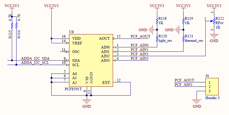
Figure 12.2 Schematics of the AD/DA converter
The schematics of AD/DA conversion using PCF8591 is shown in Figure 12.2. The IIC bus goes through two pull-up resistors and pulls high when not working. A0, A1, A2 are grounded, so the device address is 7’b1010000, the analog input channel AIN0 is connected to the photoresistor, AIN1 is connected to the thermistor, and AIN3 is connected to the potentiometer. When the channel is selected, FPGA will read the value in PCF8591 through the data bus ADDA_I2C_SLC for processing.
12.3.3 Introduction to the Program
This experiment also uses the IIC bus to control the PCF8951 chip, so the program is basically the same as Experiment 11. Only parts difference from Experiment 11 are indicated here.
| reg [7:0] read_data_temp [15:0];
reg [11:0] dis_data_temp; always @ (posedge clk) dis_data_temp <= read_data_temp[0] + read_data_temp[1] + read_data_temp[2] + read_data_temp[3] + read_data_temp[4] + read_data_temp[5] + read_data_temp[6] + read_data_temp[7] + read_data_temp[8] + read_data_temp[9] + read_data_temp[10] + read_data_temp[11] + read_data_temp[12] + read_data_temp[13] + read_data_temp[14] + read_data_temp[15]; always @ (posedge clk ) dis_data <= dis_data_temp >> 4; integer i; always @ (posedge clk or posedge rst) begin if (rst) begin for (i=0;i<16;i=i+1) read_data_temp[i] <= 8’h00; end else if (iic_done) begin for (i=0;i<15;i=i+1) read_data_temp[i+1] <= read_data_temp[i]; read_data_temp[0] <= read_data ; end else begin for (i=0;i<16;i=i+1) read_data_temp[i] <= read_data_temp[i]; end end |
The role of this part is that when the chip continuously collects the voltage value across the resistor, due to a series of unstable factors, the voltage value will be unstable, so the output value will have a large error, so 16 sets of data is collected each time, then gets averaged, and the result is output as the voltage value across the resistor at this time. Then, by the change of the voltage value, it is possible to judge the regular pattern. Such as photoresistor, the greater the light intensity, the smaller the voltage value, the smaller the resistance value, satisfying the photoresistor characteristics; the higher the thermistor temperature, the smaller the voltage value, the smaller the resistance, satisfying the photoresistor characteristics; the potentiometer rotates clockwise, and the voltage increases, the resistance increases; counterclockwise rotating decreases the voltage, and the resistance decreases.
The maximum output of the AD chip is an 8-bit digital quantity, but in fact it is not the required voltage value. It quantifies the voltage value of the range into 256 portions (8-bit binary number can represent 256 decimal numbers), so further calculations and conversions needs to be applied when displaying on the segment display.
| parameter V_REF = 12’d3300;
reg [19:0] num_t; reg [19:0] num1; wire [3:0] data0; wire [3:0] data1; wire [3:0] data2; wire [3:0] data3; wire [3:0] data4; wire [3:0] data5; assign data5 = num1 / 17’d100000; assign data4 = num1 / 14’d10000 % 4’d10; assign data3 = num1 / 10’d1000 % 4’d10 ; assign data2 = num1 / 7’d100 % 4’d10 ; assign data1 = num1 / 4’d10 % 4’d10 ; assign data0 = num1 % 4’d10;
always @ (posedge clk) num_t <= V_REF * dis_data; always @(posedge clk or posedge rst) begin if(rst) begin num1 <= 20’d0; end else num1 <= num_t >> 4’d8; end |
VCC is 3.3V, so the maximum resistance voltage is 3.3V. The 8-bit data dis_data is multiplied by 3300 and assigned to numt by 1000 times, which is convenient for display and observation. The numt is further reduced by 256 times (left shifting 8 bits) to num1, corresponding to 256 quantitized portions of PCF8951. num1 at this time is 1000 times the voltage value of two ends of the resistor. Display each digit on the segment display, in the order of high to low (data5 to data0) and add the decimal point (data3) to digit of thousands. At this time, the value displayed by the segment display is the voltage across the resistor value and correct to 3 decimal places.
12.4 Experiment Verification
The first step: pin assignments
See Table 12.2 for the pin assignmnet
Table 12.2 AD conversion experiment pin mapping
| Signal Name | Network Label | FPGA Pin | Port Description |
| clk | C10_50MCLK | 91 | System Clock 50 MHz |
| rst | KEY3 | 10 | Reset |
| sm_db[0] | SEG_PA | 132 | Segment selection signal |
| sm_db [1] | SEG_PB | 137 | |
| sm_db [2] | SEG_PC | 133 | |
| sm_db [3] | SEG_PD | 125 | |
| sm_db [4] | SEG_PE | 126 | |
| sm_db [5] | SEG_PF | 138 | |
| sm_db [6] | SEG_PG | 135 | |
| sm_db [7] | SEG_DP | 128 | |
| data[0] | SW0 | 80 | Switch input |
| data[1] | SW1 | 83 | |
| data[2] | SW2 | 86 | |
| data[3] | SW3 | 87 | |
| data[4] | SW4 | 74 | |
| data[5] | SW5 | 75 | |
| data[6] | SW6 | 76 | |
| data[7] | SW7 | 77 | |
| scl | ADDA_I2C_SCL | 53 | PCF8591 clock line |
| sda | ADDA_I2C_SDA | 52 | PCF8591 data line |
| sel[0] | SEG_3V3_D0 | 136 | Bit selection signal |
| sel[1] | SEG_3V3_D1 | 142 | |
| sel[2] | SEG_3V3_D2 | 141 | |
| sel[3] | SEG_3V3_D3 | 129 | |
| sel[4] | SEG_3V3_D4 | 127 | |
| sel[5] | SEG_3V3_D5 | 124 |
The second step: board verification
After the pin assignment is completed, the compilation is performed, and board is verified after passing.
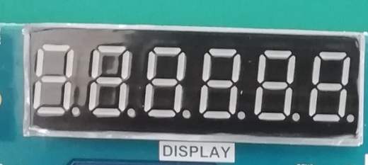
Under the default state, that is, the channel selection is “00”, the segment display shows the current ambient brightness state, the voltage value across the photoresistor is 1.469 V, as shown in Figure 12.3.
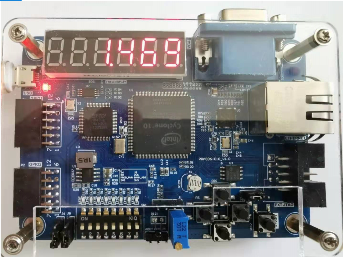
Figure 12.3 Photoresistor test phenomenon
When the channel selection is “01”, the segment display shows the current ambient temperature, the voltage across the thermistor is 2.926 V, as shown in Figure 12.4.
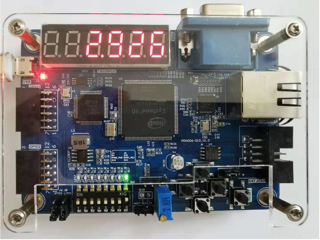
Figure 12.4 Thermistor experiment phenomenon
When the channel is selected as “10”, the segment display shows the current resistance value, and the voltage across the potentiometer is 1.624 V, as shown in Figure 12.5.
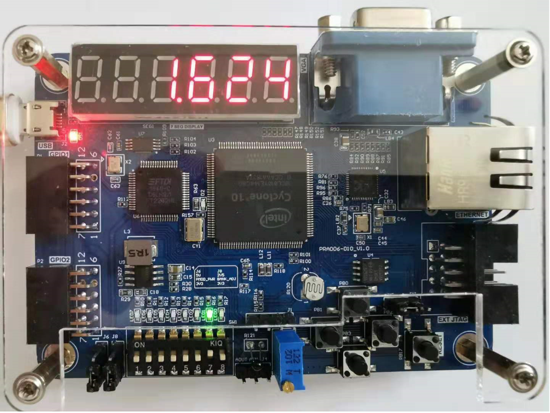
Figure 12.5 Potentiometer experiment phenomenon