Asynchronous Serial Port Communication, Handshake Mechanism and Data Frame Strcuture, Asynchronous Serial Port Design and Experiment – FPGA Beginner Study Board PRA006, PRA010 Experiment 10
Experiment 10 Asynchronous Serial Port Design and Experiment
10.1 Experiment Objective
Because asynchronous serial ports are very common in industrial control, communication, and software debugging, they are also vital in FPGA development.
- Study the basic principles of asynchronous serial port communication, handshake mechanism and data frame strcuture
- Master asynchronous sampling techniques
- Review the frame structure of the data packet
- Learn to use FIFO
- Joint debugging with common debugging software of PC (SSCOM, Tera Term, etc.)
10.2 Experiment Implement
- Design and transmit full-duplex asynchronous communication interface Tx, Rx
- Baud rate of 11520 bps, 8-bit data, 1 start bit, 1 or 2 stop bits
- Receive buffer (Rx FIFO), transmit buffer (Tx FIFO)
- Forming a data packet
- Packet parsing
10.3 Experiment
10.3.1 Inrtroduction of USB to Serial Conversion Chip (FT2232)
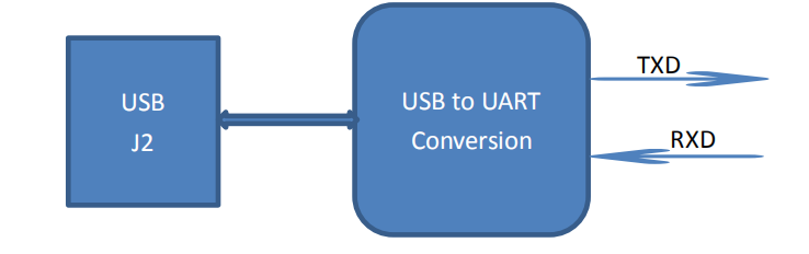
USB is an interface technology used in the PC field to regulate the connection and communication between computers and external devices. The USB interface supports plug-and-play and hot-swap capabilities for devices and connects up to 127 peripherals such as mice, modems and keyboards. However, there are still a large number of peripheral devices and software using the RS232 serial port standard. In order to fully utilize the advantages of USB, a USB-RS232 converter is designed to transmit RS232 data through the USB bus. Here is a design scheme of USB-RS232 conversion module based on FT2-232H.
The onboard serial port conversion chip is FT2232, which can realize USB to two serial UART, FIFO, Bit-Bang I/O interface, and can also be configured as MPSSE, I2C, JTAG and SPI bus. The FT2232H has two independent UART/FIFO controllers for controlling asynchronous data, 245 FIFO data, opto-isolated (high-speed serial) or controlling Bit-Bang mode when installing program commands; USB protocol engine controlling and managing the interface between UTMI PHY and FIFO. It is also responsible for power management and USB protocol specifications; the dual port FIFO TX buffer (4KB) stores data from the host PC and uses data from the multipurpose UART, FIFO controller; dual port FIFO RX buffer (4KB) Stores data from the multipurpose UART/FOFO controller and then sends the data to the host; the reset generator module provides a reliable power reset for the internal circuitry of the device when powered up. The RESETn input pin allows the external device to reset the FT2232H. If RESETn is not used, it should be connected to VCCIO (+3.3 V); the independent baud rate generator provides a ×16 or ×10 clock signal to the UART. The optimum baud rate tuning is provided by a 14-bit scale factor and 4 register bits to determine the baud rate of the UART programmable settings.
10.3.2 Hardware Design
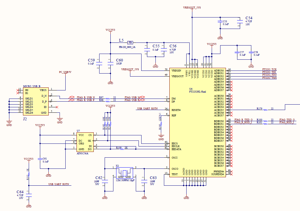
Figure 10.1 Schematics of the serial port
The schematics of USB serial port conversion is shown in Figure 10.1. J2 is a USB interface. When downloading the program, the two lines of USB_N and USB_P are input to the FT2232, and are internally processed and input into the FPGA by JTAG_TXD_O. In the serial port experiment, the transmission path from the PC end to the FPGA end is consistent with the download procedure. The FPGA to PC receive path is the FPGA transmits the data from JTAG_RXD_I to the FT2232, and is internally processed and then sent to the PC through the USB interface to implement serial receive and transmit functions.
10.3.3 Introduction to the Program
The first step: the main program architecture
| module uart_top
( input inclk, input rst, input [1:0] baud_sel, input tx_wren, input tx_ctrl, input [7:0] tx_data, input tx_done, output txbuf_rdy,
input rx_rden, output [7:0] rx_byte, output rx_byte_rdy, output sys_rst, output sys_clk, input rx_in, output tx_out ); |
There are a lot of handshake signals here, with the tx prefix for the transmit part of the signal, and the rx prefix is for the receive part of the signal.
The second step: create a new baud rate generator file
- Input clock 7.3728MHz (64 times 115200). The actual value is 7.377049 MHz, which is because the coefficient of the PLL is an integer division, while the error caused by that is not large, and can be adjusted by the stop bit in asynchronous communication. See Figure 10.2.
Fine solution
- Implemented with a two-stage PLL for a finer frequency
- The stop bit is set to be 2 bits, which can effectively eliminate the error.
This experiment will not deal with the precision. The default input frequency is 7.3728 MHz.
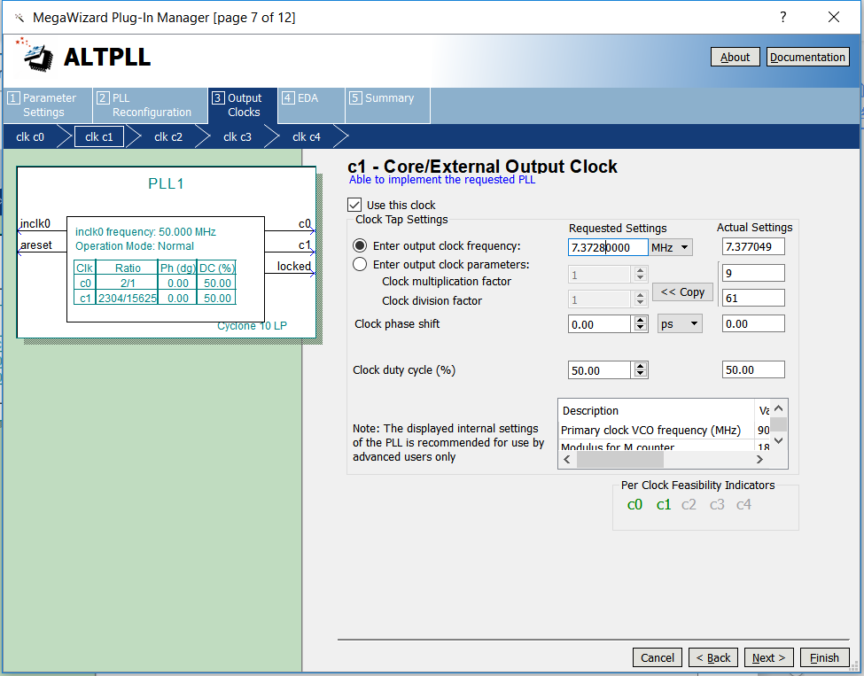
Figure 10.2 PLL setting
- Supported baud rates are 115200,57600,38400,19200
- The default baud rate is 115200
- Source file of designing baud rate
| //Transmit baud rate, clock frequency division selection
wire [8:0] frq_div_tx; assign frq_div_tx = (baud_sel == 2’b00) ? 9’d63: (baud_sel == 2’b01) ? 9’d127: (baud_sel == 2’b10) ? 9’d255:9’d511; reg [8:0] count_tx=9’d0; always @ (posedge inclk) if (rst) begin count_tx <= 9’d0; baud_tx <= 1’b0; end else begin if (count_tx == frq_div_tx) begin count_tx <= 9’d0; baud_tx <= 1’b1; end else begin count_tx <= count_tx + 1’b1; baud_tx <= 1’b0; end end |
Four different gear positions are set to select the baud rate, corresponding to the second step, (1). The baud rate of the receiving part is consistent to that of the transmitting part.
The third step: design the transmit buffer file tx_buf
- 8-bit FIFO, depth is 256, read/write clock separation, write full flag, read empty flag
- Interface and handshake
- rst reset signal
- wr_clk write clock
- tx_clk transmit clock
- 8-bit write data tx_data
- wr_en write enable
- ctrl writes whether the input is a data or a control word
- rdy buffer ready, can accept the next data frame
Transmit buffer instantiation file
| tx_buf
#(.TX_BIT_LEN(8),.STOP_BIT(2)) tx_buf_inst ( .sys_rst (sys_rst), .uart_rst (uart_rst), .wr_clk (sys_clk), .tx_clk (uart_clk), .tx_baud (tx_baud), .tx_wren (tx_wren), .tx_ctrl (tx_ctrl), .tx_datain (tx_data), .tx_done (tx_done), .txbuf_rdy (txbuf_rdy), .tx_out (tx_out) ); |
- Serial transmission, interface and handshake file design
- Interface design
- tx_rdy, send vacancy, can accept new 8-bit data
- tx_en, send data enable, pass to the sending module 8-bit data enable signal
- tx_data, 8-bit data to be sent
- tx_clk, send clock
- tx_baud, send baud rate
- Instantiation
| tx_transmit
#(.DATA_LEN(TX_BIT_LEN), .STOP_BIT(STOP_BIT) ) tx_transmit_inst ( .tx_rst (uart_rst), .tx_clk (tx_clk), .tx_baud (tx_baud), .tx_en (tx_en), .tx_data (tx_data), .tx_rdy (trans_rdy), .tx_out (tx_out) ); |
- Write a testbench file to simulate the transmit module. (tb_uart)
- ModelSim simulation waveforms for transmit module. See Figure 10.3.
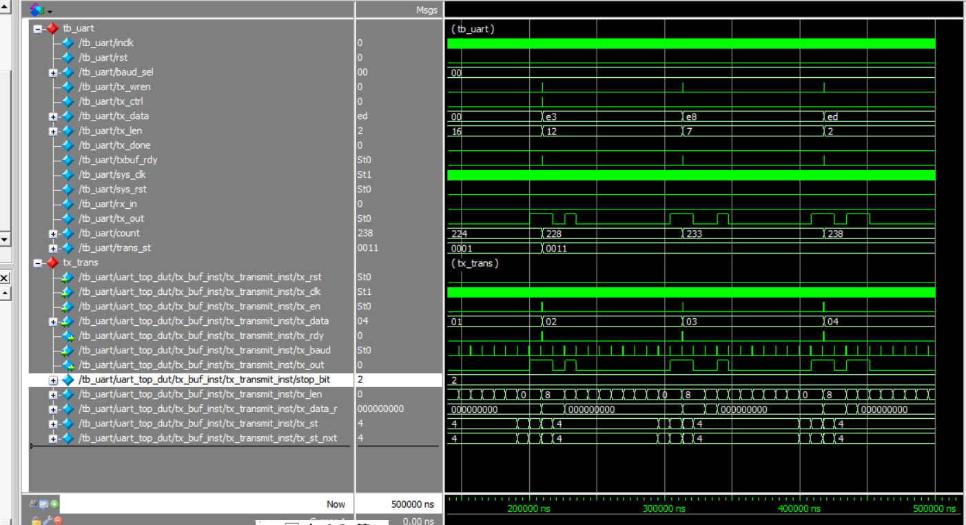
Figure 10.3 Serial port transmit ModelSim waveform
- Extended design (extended content is only reserved for users to think and practice)
- Design the transmitter to support 5, 6, 7, 8-bit PHY (Port physical layer)
- Support parity check
- The settings of the above steps involve FIFO, PLL, etc. (Refer to uart_top project file)
The fourth step: UART receiving module design
- Desigbn of rx_phy.v
- Design strategies and steps
- Use 8 times sampling: so rx_baud is different from tx_baud, here sampling is rx_band = 8*tx_band
- Adopting judgments to the receiving data
Determine whether the data counter is greater than 4 after the sampling value is counted.
- Steps to receive data:
- Synchronization: refers to how to find the start bit from the received binary data e.g. 0101 (sync_dtc)
- Receive start bit (start)
- Cyclically receive 8-bit data
- Receive stop bit (determine whether it is one stop bit or two stop bits)
- Determine if the stop bit is correct
- Correct, jump to step B
- Incorrect, jump to step A, resynchronize
- Do not judge, jump directly to B, this design adopts the scheme of no judgment
- Design of rx_buf
- Design strategies and steps
- Add 256 depth, 8-bit fifo
- Read and write clock separation
- Asynchronous clear (internal synchronization)
- Data appears before the rdreq in the read port
- Steps:
- Initialization: fifo, rx_phy
- Wait: FIFO full signal (wrfull) is 0
- Write: Triggered by rx_phy_byte, rx_phy_rdy of rx_phy:
- End of writing
- Back to step b and continue to wait
- rx_buf.v source program (Reference to project files)
- Receive module simulation
Contents and steps
- tx, rx loopback test (assign rx_in = tx_out)
- Continue to use the testbench file in the tx section
- Write the testbench of rx
- ModelSim simulation. See Figure 10.4.
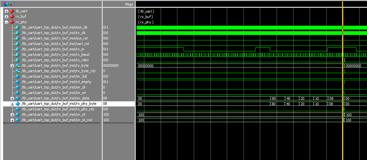
Figure 10.4 rx_phy waveform
- Reflection and development
- Modify the program to complete the 5, 6, 7, 8-bit design
- Completing the design of the resynchronization when the start and stop have errors of the receiving end rx_phy
- Complete the analysis and packaging of the receiving data frame of rx_buf
- Using multi-sampling to design 180° alignment data sampling method, compare FPGA resources, timing and data recovery effects
10.4 Experiment Verification
- Hardware interface, FII-PRA006/010 development board has intergrated USB to serial port conversion
- See Table 10.1 for the FPGA and UART pin assignment.
Table 10.1 FPGA and UART pin mapping
| UART Name | RXD | TXD |
| Network Label | JTAG_TXD_O | JTAG_RXD_I |
| FPGA Pin | 144 | 143 |
- Write a hardware test file
- Test plan: connect development board J2 to host USB interface
- Using test software such as Tera Term, SSCOM3, etc., you can also write a serial communication program (C#, C++, JAVA, Python…)
- PC sends data in a certain format
- The test end uses a counter to generate data in a certain format.
- Write the test program hw_tb_uart and instantiate uart_top in it.
- et hw_tb_uart to the top level, instantiate the previous program, and then verify it
- Pin assignments:
The pin assignment is shown in Tabel 10.2.
Table 10.2 Serial port experiment pin mapping
| Signal Name | Network Label | FPGA Pin | Port Description |
| Inclk | C10_50MCLK | 91 | Input clock |
| rst | KEY2 | 10 | Reset |
| rx_in | TAG_RXD_I | 144 | Serial data received |
| tx_out | TAG_TXD_O | 143 | Serial data transmitted |
- Observe the experiment result
- Observe the data received by the PC. See in Figure 10.5.
- Observe the data received by the FPGA with SignalTap II
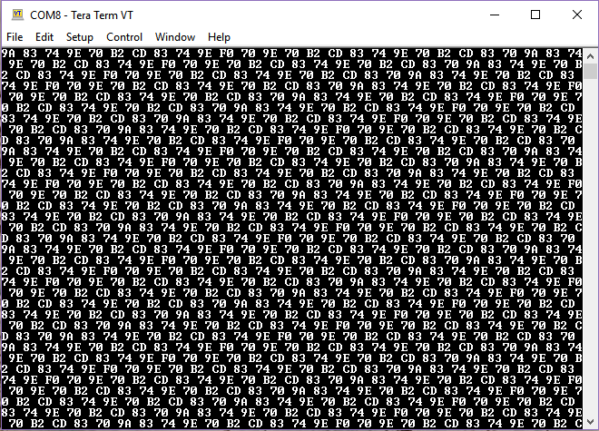
Figure 10.5 Data transmitted by FPGA displayed on the host computer
- The receiving part has been skipped here. It is encouraged to try it personaly.