Description
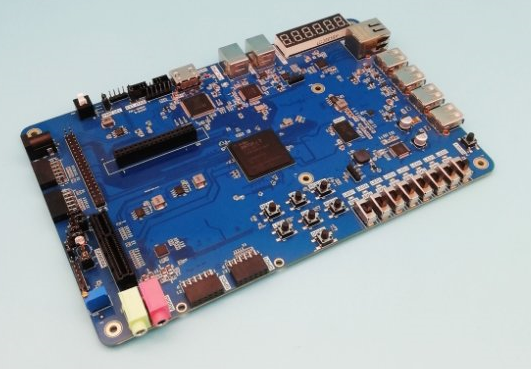
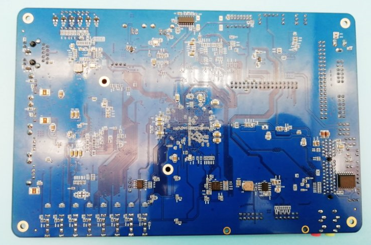
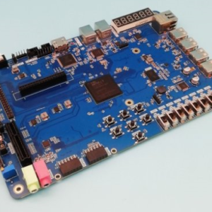
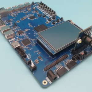
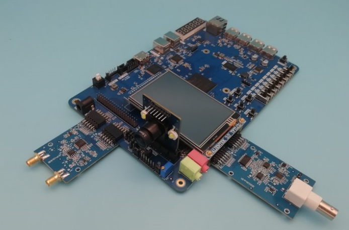
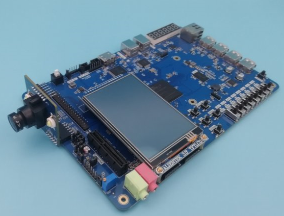
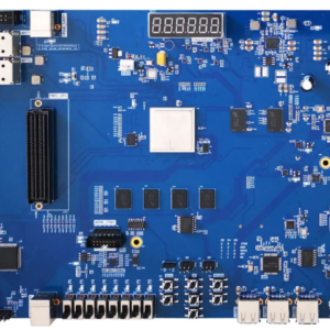
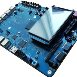
FII-PRX100-D Risc-V FPGA Board is a ready-to-use development platform designed around the Field Programmable Gate Array (FPGA) from Xilinx.
It was designed to cover all aspects of FPGA Development and Experiment, RISC-V SOC . The main application areas aim at smart home, Wearable, sensor Fusion, IOT, and industrial control etc.
FII-PRX100-D Risc-V FPGA Board is a ready-to-use development platform designed around the Field Programmable Gate Array (FPGA) from Xilinx. It was designed to cover all aspects of FPGA Development and Experiment, RISC-V SOC . The main application areas aim at smart home, Wearable, sensor Fusion, IOT, and industrial control etc.
Features:
|
|
The entire system is designed by the verilog language, and all IPs can be added, deleted and reconfigured.
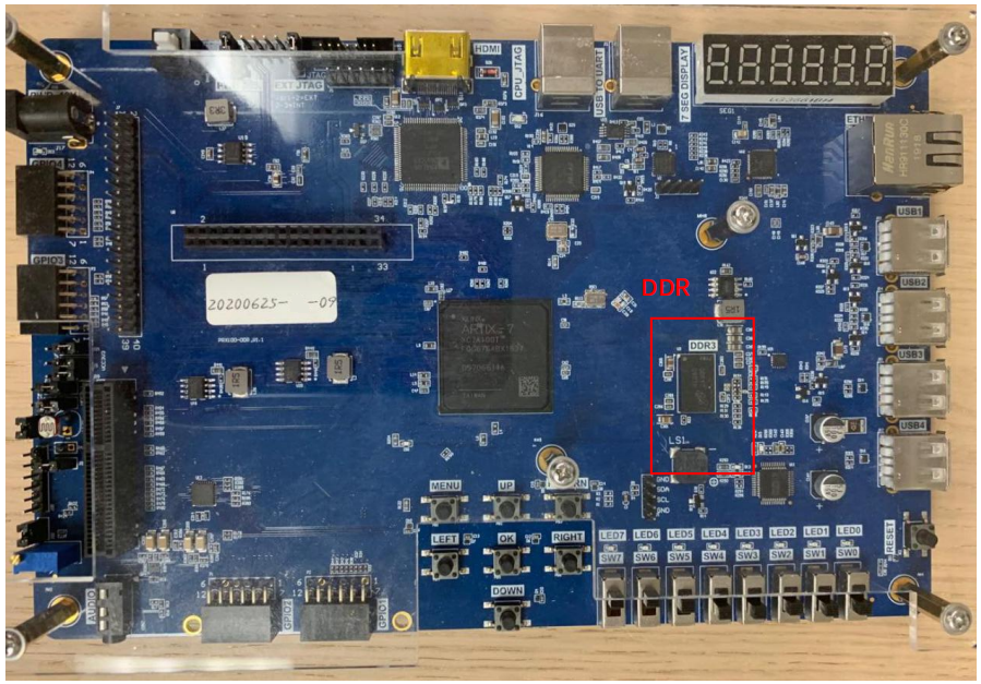
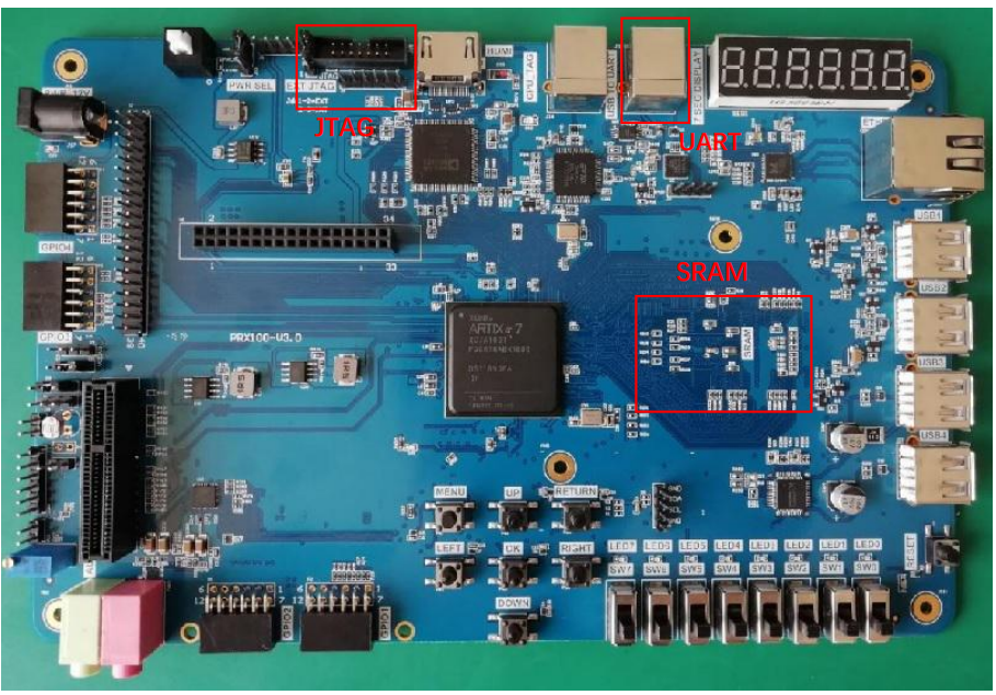
The FII-PRX100-D RISC-V development board introduction
- Suitable for FPGA study and training
- Fully support FIE310 CPU running and system development
- Suitable for user customized RV32G verification and validation
- JTAG interface for FPGA and FIE310 CPU download and debug
- Support Windows software and linux development environment
- GCC compilation toolchain and graphical software development environment
- Hardware resource: Switchs, Push Button ,USB to UART convertor, QSPI flash, I2C EEPROM, 100M/1G ethernet, USB keyboard mouse,GPIO , hdmi transmitter and camera etc.
RISC-V IPCore user development Guide
This document is edited by Fraser Innovation Inc. Step by step introduce how to develop each RISC-V CPU RTL modules based on RISC-V ISA, Simulations and board verifications, software environment and details on C language development, debug and program
Artificial Intelligence
Voice collection, speech recognition
Image acquisition and image recognition, deep learning
IOT
FII-PRX100-D Risc-V FPGA Board Product Features:
- FPGA part: XC7A100T-2FGG676I
- 1MSPS On-chip: yes
- Logic Cells: 101440
- Logic Slices: 15850
- Flip-flops: 65200
- Memory blocks(36K): 135
- Memory block(Kb): 4860
- Clock Management Tiles: 6
- DSP Slices: 240
System Features:
- ADC: On-chip analog-to-digital converter (XADC)
- DRAM: DDR3 MT41J128M16HA-125 ( Micron Technology LTD )
- Clock Frequency: 800MHZ
- Memory Size: 2GB (128M X 16)
- Spi Flash: serial flash (16M bytes)
- JTAG: jtag Programmable ports
- Multifunction: used for other board (For example: iMX226 camera board, or adv7612 Hdmi in board , etc)
- Power Supply: 12V adapter source

Interaction and Sensory Devices:
- 8 Switches
- 7 Buttons (up , down, left, right, ok, menu, return)
- 1 Reset button
- 8 LEDs
- 1 4-digit 7 segment display
- 1 I2c interface (24c02 eeprom)
-
Expansion Connector:
- 4 gpio connectors (compatible with digilent Pmod)
- 2 MultiFunction connectors (connect with iMX226 board, or others)
- Main Chips: xilinx (1.0mm pitch) XC7A100T_FGG676
Interaction and Sensory Devices
- GPIO Interface (16 ) 2×8 Standard 2.54mm connector (pin)
- led output (8 ) 0603 SMD
- 8 switchs SMD
- 7 buttons (Top, Bottom, left, right,center, top left (menu), top right (return)
- i2c 24c02 smd soic
- spi flash MX25L6433F 8-SOP (8M bytes)
- usb2uart ft2232C/H (2 uart ) Or cp2102 (1 uart)
- jtag 2×5 Standard 2.54mm connectors(pin)
- eth 1G CAT5 Ethernet (rtl8111e)
- sram IS61WV25616 (2 pieces ) 256K x 32bit
- Digital tube 7seg (4) oasistek TOF-5421BMRL-N
- Hdmi out adv7511, hdmi_adv7511.SchDoc
- Test Port: 1×6 Standard2.54mm Connectors (pin)
We will send you following Documents after you have bought from us:
Risc-V Board PRX100-D Experimental Manual
Risc-V Board PRX100-D Schematic Diagram
Risc-V Board PRX100-D Hardware Configuration
FII-PRX100-D Development Board ( ARTIX 100T, XC7A100T, RISC-V FPGA Developing Board)
Online Shopping:
https://fpgamarketing.com/FII-PRX100-D-ARTIX-100T-XC7A100T-RISC-V-FPGA-Board-PRX100-D-1.htm
-
FII-PRX100-D RISC-V development board
- Suitable for FPGA study and training
- Fully support FIE310 CPU running and system development
- Suitable for user customized RV32G verification and validation
- JTAG interface for FPGA and FIE310 CPU download and debug
- Support Windows software and linux development environment
- GCC compilation toolchain and graphical software development environment
- Hardware resource: Switchs, Push Button ,USB to UART convertor, QSPI flash, I2CEEPROM, 100M/1G ethernet,USB keyboard mouse,GPIO, hdmi transmitter and camera etc.
1.System Design Objective
The main purpose of this system design is to complete FPGA learning, development and experiment with Xilinx-Vivado. The main device uses the Xilinx-XC7A100T-2FGG676I and is currently the latest generation of FPGA devices from Xilinx. The main learning and development projects can be completed as follows:
- Basic FPGA design training
- Construction and training of the SOPC (Microblaze) system
- IC design and verification, the system provides hardware design, simulation and verification of RISC-V CPU
- Development and application based on RISC-V
- The system is specifically optimized for hardware design for RISC-V system applications.
2.System Resource
-
- Extended memory
- Use two Super Srams in parallel to form a 32-bit data interface with a maximum access space of 1M bytes.
- IS61WV25616 (2 pieces) 256K x 32bit
- Serial flash
- Spi interface serial flash (128M bytes)
- Serial EEPROM
- Gigabit Ethernet: 100/1000 Mbps
- USB to serial interface: USB-UART bridge
3.Human-computer Interaction Interface
-
- 8 toggle switches
- 8 push buttons
- Definition of 7 push buttons: up, down, left, right, ok, menu, return
- 1 for rest: Reset button
- 8 LEDs
- 6 7-segment decoders
- I2C bus interface
- UART external interface
- JTAG programming interfaces
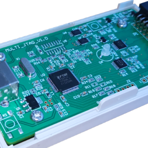
- Integrated FPGA Jtag and Risc-V Jtag by using single USB port.
- Built-in RISC-V IPCore
- CPU software debugger, no external RISC-V JTAG emulator required
- 12-pin GPIO connectors, in line with PMOD interface compatible.
4 Software Development System
- Vivado 18.1 and later version for FPGA development, Microblaze SOPC
- Freedom Studio-Win_x86_64 Software development for RISC-V CPU
5. Supporting Resources
-
- RISC-V JTAG Debugger
- Xilinx Altera JTAG Download Debugger
- FII-PRX100-D Development Guide
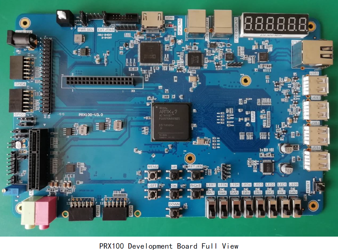
The Artix-7 is one of the Xilinx 28nn FPGA families. It features a small form factor package that reduces the power consumption of the Artix-7 family by half compared to the Spartan-6 family.
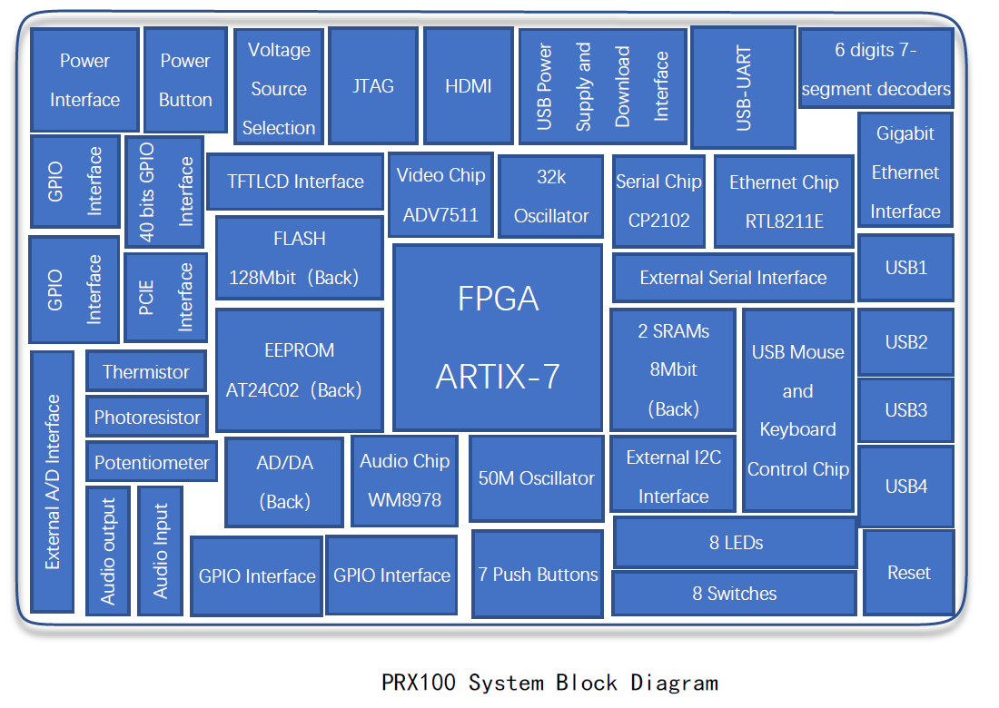
PRX100 system block diagram:
PRX100 Hardware resources:
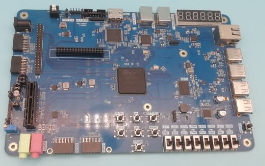
- It can be powered by external 12V DC source or by “USB Power Supply and Download Interface”. The latter also provides program download functionality. Only one wire is to complete the power supply and download functions;
- A 50 MHz oscillator, a 32.768 kHz oscillator, provides a stable clock source for the development board;
- 6-digit common anode 7-segment decoders, through dynamic scanning to achieve data display;
- 1 HDMI interface displaying color pictures or camera video;
- 1 chip I2C interface EEPROM chip, model AT24C02;
- 1 adaptive 10 M/100M/Gigabit Ethernet interface;
- 8 push buttons, 7 for programmable buttons, 1 for reset button;
- 1 photoresistor, through which it can simulate light control; 1 thermistor, which can collect temperature or analog temperature alarm function; 1 potentiometer, which can simulate voltage change;
- 1 PCF8591 AD/DA conversion chip, reserved external interface, free input and output;
- Onboard 50MHz and 32.768kHz oscillators provide stable clock signals to the development board;
- 8-bit DIP switch;
- 8-bit LED;
- 1 128Mbit Flash chip;
- 4 GPIO external signal expansion interfaces, also the PMOD standard interface;
- A 40-pin GPIO expansion interface that provides a large amount of I/O for developers to use freely;
- Two JTAG interfaces, one for the FPGA download debug interface (J4, J5) and one for the RISC-V CPU JTAG debug interface(J16). Built-in RISC-V CPU software debugger, no external RISC-V JTAG emulator required;
- 1 UART asynchronous serial interface;
- 2 SRAMs with a capacity of 8Mbit;
- a pair of audio input and output interfaces;
- 1 PCIE interface;
- 4 USB interfaces, 2 for the mouse and keyboard interface, 2 for the universal serial interface;
- 1 USB (USB-B) to UART interface for serial communication;
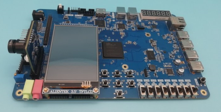
- 1 TFTLCD touch screen interface, which can realize the display and operation of the touch screen;
RISC-V FPGA Board – FII-PRX100-S Experimental Manuals – Study Guide (V1.1)
-
-
- xilinx Risc-V FPGA Board – FII-PRX100 – Development System Introduction
- Risc-V FPGA Board Xilinx – Development Board Experiment 1 – LED Shifting – FII-PRX100
- Xilinx Risc-V Board Tutorial : Switches and Display – FII-PRX100 FPGA Board Experiment 2
- Xilinx Risc-V Board Tutorial : Basic Digital Clock Experiment and Programming of FPGA Configuration Files- FII-PRX100 FPGA Board Experiment 3
- Xilinx Risc-V Board Tutorial : Block/SCH Digital Clock Design- FII-PRX100 FPGA Board Experiment 4
- Xilinx Risc-V Board Tutorial : Button Debounce Design and Experimental- FII-PRX100 FPGA Board Experiment 5
- Xilinx Risc-V Board Tutorial : Digital Clock Comprehensive Design Experiment- FII-PRX100 FPGA Board Experiment 6
- Xilinx Risc-V Board Tutorial : Multiplier Use and ISIM Simulation- FII-PRX100 FPGA Board Experiment 7
- Xilinx Risc-V Board Tutorial : Hexadecimal Number to BCD Code Conversion and Application – FII-PRX100 FPGA Board Experiment 8
- Xilinx Risc-V Board Tutorial : Use of ROM – FII-PRX100 FPGA Board Experiment 9
- Xilinx Risc-V Board Tutorial : Use Dual_port RAM to Read and Write Frame Data – FII-PRX100 FPGA Board Experiment 10
- Xilinx Risc-V Board Tutorial : Asynchronous Serial Port Design and Experiment – FII-PRX100 FPGA Board Experiment 11
- Xilinx Risc-V Board Tutorial : IIC Protocol Transmission – FII-PRX100 FPGA Board Experiment 12
- Xilinx Risc-V Board Tutorial : AD, DA Experiment – FII-PRX100 FPGA Board Experiment 13
- Xilinx Risc-V Board Tutorial : HDMI Graphic Display Experiment – FII-PRX100 FPGA Board Experiment 14
- How ethernet work and familiar with MII, GMII, RGMII interface types – FII-PRX100 Risc-V Board Experiment 15
- Audio 8978 Loopback Experiment – What is I2S (Inter-IC Sound) bus and how it works – AWM8978 Audio Boardudio – Xilinx Risc-V FII-PRX100 Board Experiment 16
- Reading Experiment of Serial Port Partition of Static Memory SRAM, Read and write timing of IS61WV25616BLL SRAM, and prepare for the next experimental experiment of OV5640 camera experiment – – Xilinx Risc-V FII-PRX100 Board Experiment 17
- Photo Display Experiment of OV5640 Camera , Understand the power-on sequence of the OV5640 camera and the corresponding register configuration process – Xilinx Risc-V Board FII-PRX100 Experiment 18
- High-speed ADC9226 Acquisition Experiment – Xilinx Risc-V Board FII-PRX100 Experiment 19
-
-
The Newest Xilinx Risc-V Board FII-PRX100-S, FII-PRX100-D Experiment Manuals with 20 experiments.
- Loading...
Loading...







Reviews
There are no reviews yet.