Experimental Manuals FPGA Tutor PRX100 Risc-V

Verilog HDL program to achieve frequency division, Write Verilog HDL program to implement LED shifting – Risc-V FPGA Board Xilinx – Development Board Experiment 1 – LED Shifting – FII-PRX100

Experiment 1 LED Shifting 1. Experiment Object Practice how to use the development system software Vivado to establish a new project, call the system resource PLL to establish the clock. Write Verilog HDL program to achieve frequency division Write Verilog HDL program to implement LED shifting Combine hardware resources for FPGA pin configuration Compile Download the program to the develop board Observe the experimental result and debug the project 2. Create A New Project Under Vivado Start Vivado in the start Menu. See Fig 1. 1 Fig 1. 1 Start…

Read More
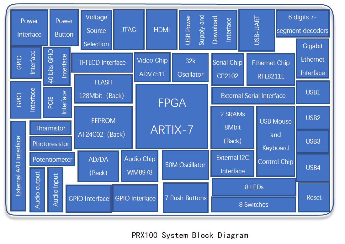
prx100 system block diagram
Experimental Manuals FPGA Tutor PRX100 Risc-V

xilinx Risc-V FPGA Board – FII-PRX100 – FPGA Development Board System Introduction

  FII-PRX100 Development Board ( ARTIX 100T, XC7A100T, RISC-V FPGA Developing Board) Online Shopping: https://fpgamarketing.com/FII-PRX100-ARTIX-100T-XC7A100T-RISC-V-FPGA-Board-PRX100-1.htm Fraser Innovation Inc develops FII-PRX100 based on the boards of the Xilinx ARTIX-7 series. It was initial released in 2018. This development board is resource-rich and high-speed, making it an ideal platform for learning and engineering research. This development board has been spent a lot on system design, PCB design, and function creation. It could even be said comprehensive and powerful. System Design Objective The main purpose of this system design is to complete FPGA learning,…

Read More
FPGA for Beginners FPGA Tutor PRA006/PRA010

interface types (MII, GMII, RGMII) advantages and disadvantages – Ethernet Experiment – FPGA Board for Beginner – Experiment 14

Experiment 14 Ethernet Experiment 14.1 Experiment Objective Understand what Ethernet is and how it works Familiar with the relationship between different interface types (MII, GMII, RGMII) and their advantages and disadvantages (our development board uses RGMII) Combine the development board to complete the transmission and reception of data and verify 14.2 Experiment Requirement Perform a loopback test to check if the hardware is working properly. Performing data verification Perform data transmission verification 14.3 Experiment 14.3.1 Experiment Principle Ethernet is a baseband LAN technology. Ethernet communication is a communication method that…

Read More
SignalTap II simulation
FPGA Board Based FPGA for Beginners FPGA Tutor Pocket Boards PRA006/PRA010

Use Dual-port RAM to Read and Write Frame Data, use synchronous (or asynchronous ) clock to control the synchronization of frame structure – FPGA Board Beginner Tutorial – Experiment 9

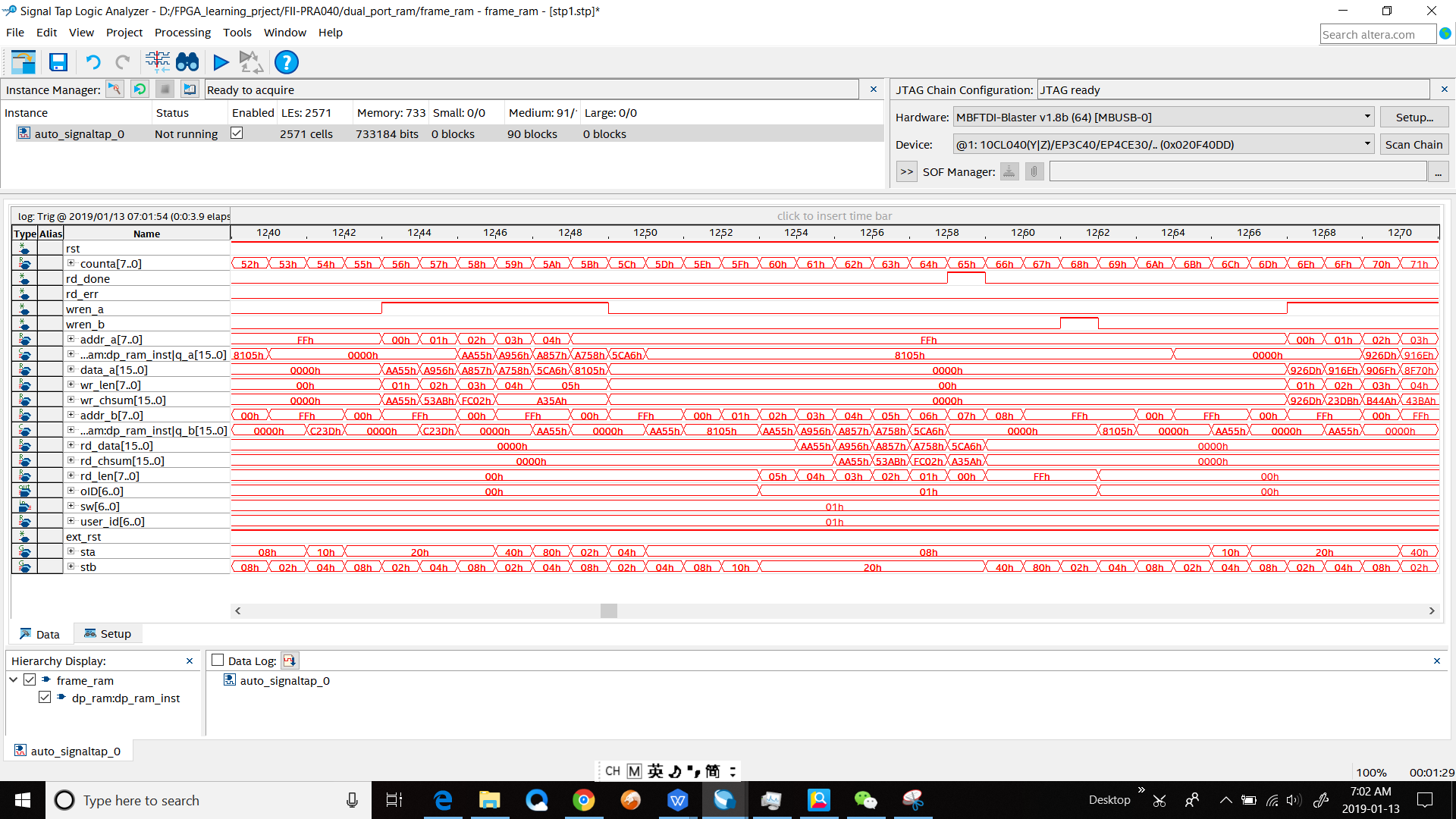
Experiment 9 Use Dual_port RAM to Read and Write Frame Data 9.1 Experiment Objective Learn to configure and use dual-port RAM Learn to use synchronous clock to control the synchronization of frame structure Learn to use asynchronous clock to control the synchronization of frame structure Experiment Implement Observing the synchronization structure of synchronous clock frames using SignalTap II Extended the use of dual-port RAM Design the use of three-stage state machine Design a 16-bit data frame Data is generated by an 8-bit counter: Data={~counta,counta} The ID of the data frame…

Read More
Learn How to use ROM
FPGA Board Based FPGA for Beginners FPGA Tutor Pocket Boards PRA006/PRA010

Design 16 outputs ROM, Study the format of *.mif and how to edit *.mif file to configure the contents of ROM, Use of ROM (Read-only Memory) – FPGA Board for Beginner Tutorial – Experiment 8

Experiment 8 Use of ROM 8.1 Experiment Objective Study the internal memory block of FPGA Study the format of *.mif and how to edit *.mif file to configure the contents of ROM Learn to use RAM, read and write RAM 8.2 Experiment Implement Design 16 outputs ROM, address ranging 0-255 Interface 8-bit switch input as ROM’s address Segment display illustrates the contents of ROM and require conversion of hexadecimal to BCD output. 8.3 Experiment 8.3.1 Introduction to Program This experiment was carried out on the basis of Experiment 7, and…

Read More
Hexadecimal Numbers to BCD Code(hex_to_bcd), binary numbers to BCD code (bin_to_bcd) Conversion and Application
FPGA for Beginners FPGA Tutor Pocket Boards PRA006/PRA010

Hexadecimal Numbers to BCD Code(hex_to_bcd), binary numbers to BCD code (bin_to_bcd) Conversion and Application – FPGA Board for Beginner Tutorial – Experiment 7

Experiment 7 Hexadecimal Number to BCD Code Conversion and Application Experiment Objective Learn to convert binary numbers to BCD code (bin_to_bcd) Learn to convert hexadecimal numbers to BCD code (hex_to_bcd) 7.2 Experiment Implement Combined with experiment 6, display the results of the operation to the segment display. 7.3 Experiment 7.2.1 Introduction to the Principle of Converting Hexadecimal Number to BCD Code Since the hexadecimal display is not intuitive, decimal display is more widely used in real life. Human eyes recognition is relatively slow, so the display from hexadecimal to decimal…

Read More
signal Tap Setting
FPGA for Beginners FPGA Tutor Pocket Boards PRA006/PRA010

Switch and Use SignalTap II Logic Analyzer in Quartus ( Verilog HDL code ), Learn to analyze the captured signals – FPGA for Beginner Tutorial – Experiment 2 – FII-PRA006

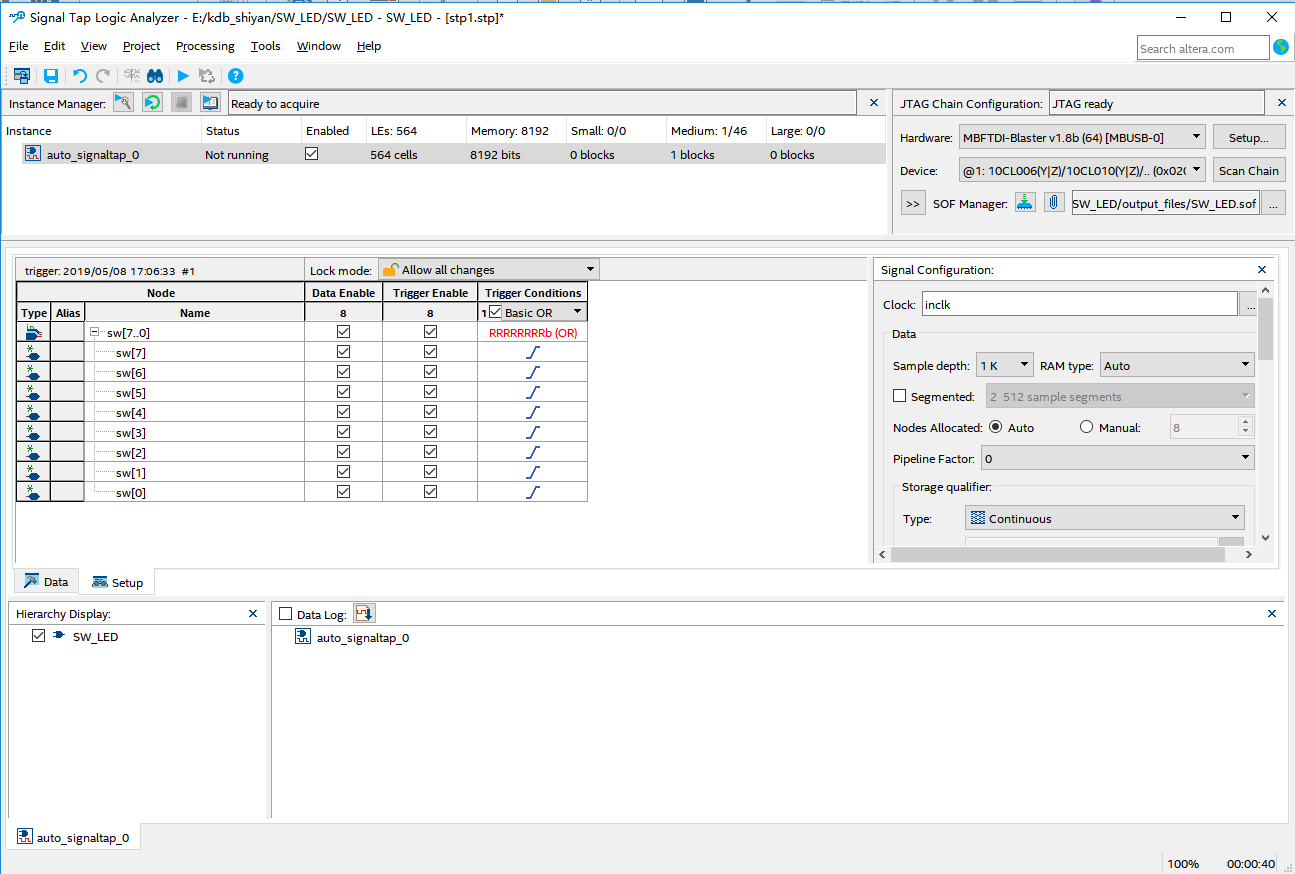
2.1 Experiment Objective  Continue to practice using the develop board  Use SignalTap II Logic Analyzer in Quartus Use FPGA configuration memory to program 2.2 Experiment Requirement By using SignalTap II, learn to analyze and capture the experimental signals. 2.3 Experiment 2.3.1 Project Building Refer to Experiment1, the following experiment project building steps will be eliminated. 2.3.2 PCB Schematics 2.3.3 Experiment Procedure We include the PLL1 generated in Experiment 1 Verilog HDL code is as follows: 2.3.4 SignalTap II Logic Analyzer Step 1: SignalTap II startup and basic setup Tools >…

Read More