Experimental Manuals FPGA Board Based FPGA for Beginners PRA006/PRA010

Building new FPGA Projects in Quartus, Device Selection, PLL setup, PLL Frequency Setting, Verilog’s Tree Hierarchy Design, and the Use of SignalTap II – Block/SCH Experiment – FPGA Beginner Study Board PRA006, PRA010 Experiment 4

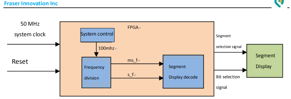
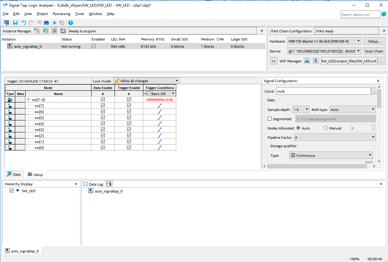
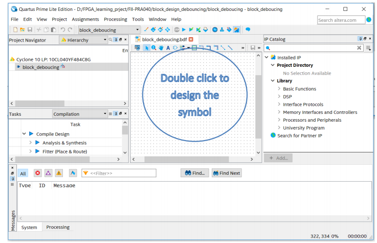
Experiment 4 Block/SCH Experiment 4.1 Experiment Objective Review building new FPGA projects in Quartus, device selection, PLL setup, PLL frequency setting, Verilog’s tree hierarchy design, and the use of SignalTap II Master the design method of graphics from top to bottom Combined with the BCD_counter project to achieve the display of the digital clock Observe the experimental results 4.2 Experiment Implement Use schematics design to build the project 4.3 Experiment This experiment is mainly to master another design method. The other design contents are basically the same as the experiment…

Read More
Experimental Manuals FPGA Board Based FPGA for Beginners FPGA Tutor PRA006/PRA010

Use the BCD Code Counter, Digital Display Decoding Design, the Serial Flash, – Segment Display – FPGA Beginner Study Board PRA006, PRA010 Experiment 3

Experiment 3 Segment Display 3.1 Experiment Objective Review previous experiments, proficient practice in PLL configuration, frequency division design, and project verification; Learn to use the BCD code counter; Digital display decoding design; Learn to program the project into the serial FLASH of the development board; 3.2 Experiment Implement The segment display has two lower (right most) digits to display seconds, the middle two digits to display minutes, and the highest (left most) two digits to display hours. The decimal point remains off and will not be considered for the time…

Read More
Signal Tap setting
Experimental Manuals FPGA Board Based FPGA for Beginners FPGA Tutor PRA006/PRA010

The Use of SignalTap Logic Analyzer, Analyze the Captured Signals – FPGA Beginner Study Board PRA006, PRA010 Experiment 2

Experiment 2 SignalTap 2.1 Experiment Objective Continue to practice using of the development board hardware; Practice the use of SignalTap Logic Analyzer in Quartus; Learn to analyze the captured signals. 2.2 Experiment Implement Capture and analyze the switching signals on the development board through the use of SignalTap. 2.3 Experiment 2.3.1 Introduction to the Switches and SignalTap Introduction to the switches The on-board switch is 8 DIP switches, as shown in Figure 2.1. The switch is used to switch the circuit by turning the switch handle using the binary coding…

Read More
Schematics of LED
FPGA for Beginners PRA006/PRA010

LED shifting, Using Quartus, the Writing of Verilog HDL programs, Mange FPGA Pin Assignment – FPGA Beginner Study Board PRA006, PRA010 Experiment 1

Experiment 1 LED shifting 1.1 Experiment Objective Practice using the development software Quartus, the building of new projects, and the use of system resources IP Core; Proficiency practice in the writing of Verilog HDL programs to develop a fine code writing style; Master the design of the frequency divider to realize the design of LED shifting; Mange FPGA pin assignment according to the schematics, and verify it though programming the development board; Observe and summarize the experiment result 1.2 Experiment Implement All LEDs are lit up when pressing self-defined reset…

Read More
Experimental Manuals FPGA for Beginners FPGA Tutor Pocket Boards PRA006/PRA010

FPGA for Beginner Board Experimental Manuals and Study Guide – PRA006, PRA010 FPGA Beginner Study Board

Fraser Innovation Inc   FII-PRA006/010 User Experimental Manual Version Control Version Date Descrption V1.0 10/07/2019 Initial Release V1.1 12/07/2019 Add figures for corresponding experimental phonomena of experiment board V1.2 30/08/2019 Modify part of pin assignments and Ethernet description   Project Files Content Experiment 1: LED_shifting Experiment 2: SW_LED Experiment 3: BCD_counter Experiment 4: block_counter Experiment 5: block_debouncing Experiment 6: mult_sim Experiment 7: HEX_BCD, HEX_BCD_mult Experiment 8: memory_rom Experiment 9: dual_port_ram Experiment 10: UART_FRAME Experiment 11: eeprom_test Experiment 12: adda_test Experiment 13: vga Experiment 14: Ethernet Part One: Introduction to FII-PRA006/010…

Read More
FPGA for Beginners FPGA Tutor PRA006/PRA010

interface types (MII, GMII, RGMII) advantages and disadvantages – Ethernet Experiment – FPGA Board for Beginner – Experiment 14

Experiment 14 Ethernet Experiment 14.1 Experiment Objective Understand what Ethernet is and how it works Familiar with the relationship between different interface types (MII, GMII, RGMII) and their advantages and disadvantages (our development board uses RGMII) Combine the development board to complete the transmission and reception of data and verify 14.2 Experiment Requirement Perform a loopback test to check if the hardware is working properly. Performing data verification Perform data transmission verification 14.3 Experiment 14.3.1 Experiment Principle Ethernet is a baseband LAN technology. Ethernet communication is a communication method that…

Read More
SignalTap II simulation
FPGA Board Based FPGA for Beginners FPGA Tutor Pocket Boards PRA006/PRA010

Use Dual-port RAM to Read and Write Frame Data, use synchronous (or asynchronous ) clock to control the synchronization of frame structure – FPGA Board Beginner Tutorial – Experiment 9

Experiment 9 Use Dual_port RAM to Read and Write Frame Data 9.1 Experiment Objective Learn to configure and use dual-port RAM Learn to use synchronous clock to control the synchronization of frame structure Learn to use asynchronous clock to control the synchronization of frame structure Experiment Implement Observing the synchronization structure of synchronous clock frames using SignalTap II Extended the use of dual-port RAM Design the use of three-stage state machine Design a 16-bit data frame Data is generated by an 8-bit counter: Data={~counta,counta} The ID of the data frame…

Read More
Learn How to use ROM
FPGA Board Based FPGA for Beginners FPGA Tutor Pocket Boards PRA006/PRA010

Design 16 outputs ROM, Study the format of *.mif and how to edit *.mif file to configure the contents of ROM, Use of ROM (Read-only Memory) – FPGA Board for Beginner Tutorial – Experiment 8

Experiment 8 Use of ROM 8.1 Experiment Objective Study the internal memory block of FPGA Study the format of *.mif and how to edit *.mif file to configure the contents of ROM Learn to use RAM, read and write RAM 8.2 Experiment Implement Design 16 outputs ROM, address ranging 0-255 Interface 8-bit switch input as ROM’s address Segment display illustrates the contents of ROM and require conversion of hexadecimal to BCD output. 8.3 Experiment 8.3.1 Introduction to Program This experiment was carried out on the basis of Experiment 7, and…

Read More
Hexadecimal Numbers to BCD Code(hex_to_bcd), binary numbers to BCD code (bin_to_bcd) Conversion and Application
FPGA for Beginners FPGA Tutor Pocket Boards PRA006/PRA010

Hexadecimal Numbers to BCD Code(hex_to_bcd), binary numbers to BCD code (bin_to_bcd) Conversion and Application – FPGA Board for Beginner Tutorial – Experiment 7

Experiment 7 Hexadecimal Number to BCD Code Conversion and Application Experiment Objective Learn to convert binary numbers to BCD code (bin_to_bcd) Learn to convert hexadecimal numbers to BCD code (hex_to_bcd) 7.2 Experiment Implement Combined with experiment 6, display the results of the operation to the segment display. 7.3 Experiment 7.2.1 Introduction to the Principle of Converting Hexadecimal Number to BCD Code Since the hexadecimal display is not intuitive, decimal display is more widely used in real life. Human eyes recognition is relatively slow, so the display from hexadecimal to decimal…

Read More
signal Tap Setting
FPGA for Beginners FPGA Tutor Pocket Boards PRA006/PRA010

Switch and Use SignalTap II Logic Analyzer in Quartus ( Verilog HDL code ), Learn to analyze the captured signals – FPGA for Beginner Tutorial – Experiment 2 – FII-PRA006

2.1 Experiment Objective  Continue to practice using the develop board  Use SignalTap II Logic Analyzer in Quartus Use FPGA configuration memory to program 2.2 Experiment Requirement By using SignalTap II, learn to analyze and capture the experimental signals. 2.3 Experiment 2.3.1 Project Building Refer to Experiment1, the following experiment project building steps will be eliminated. 2.3.2 PCB Schematics 2.3.3 Experiment Procedure We include the PLL1 generated in Experiment 1 Verilog HDL code is as follows: 2.3.4 SignalTap II Logic Analyzer Step 1: SignalTap II startup and basic setup Tools >…

Read More