FPGA for Beginner Board Experimental Manuals and Study Guide – PRA006, PRA010 FPGA Beginner Study Board
Fraser Innovation Inc
FII-PRA006/010 User Experimental Manual
Version Control
| Version | Date | Descrption |
| V1.0 | 10/07/2019 | Initial Release |
| V1.1 | 12/07/2019 | Add figures for corresponding experimental phonomena of experiment board |
| V1.2 | 30/08/2019 | Modify part of pin assignments and Ethernet description |
Project Files Content
Experiment 1: LED_shifting
Experiment 2: SW_LED
Experiment 3: BCD_counter
Experiment 4: block_counter
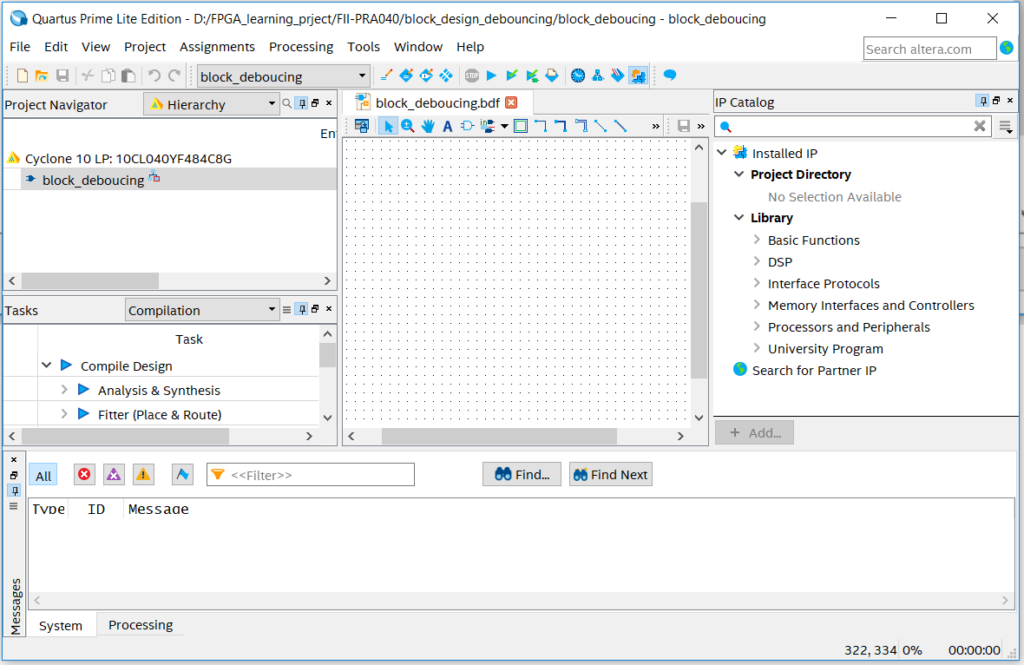
Experiment 5: block_debouncing
Experiment 6: mult_sim
Experiment 7: HEX_BCD, HEX_BCD_mult
Experiment 8: memory_rom
Experiment 9: dual_port_ram
Experiment 10: UART_FRAME
Experiment 11: eeprom_test
Experiment 12: adda_test
Experiment 13: vga
Experiment 14: Ethernet
Part One: Introduction to FII-PRA006/010
Design Objective for the System
The main purpose of designing this system is to achieve FPGA learning, development and experiment with Intel Quartus. The main device is Intel Cyclone10 10CL006YE144C8G or 10CL010YE144C8G, and is currently the latest generation of FPGA devices from Intel. The main learning and development projects can be completed as follows:
(1)Basic FPGA design practice
(2)Construction and practice using of SOPC (NIOSII) system.
(3)As a fully functional development board, PRA006/010 can also be used as a downloader to provide download services for Altera, Xillinx, and Risc-V.
System Resources
(1)Serial flash
Spi interface: serial flash (16M bytes)
(2)Serial EEPROM
(3)Gigabit Ethernet: 100/1000 Mbps
(4)USB to serial interface: USB-UART bridge
3、Human-computer Interaction Switch
(1)8 DIP switches
(2)5 buttons
4 buttons are defined as (up, down, left, right), the other one is the reset button
(3)8 LEDs
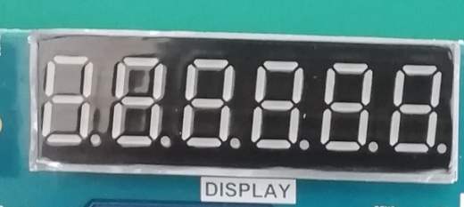
(4)6 seven-segment display
(5)I2C bus interface
(6)USB to UART interface
(7)JTAG programming interface
(8)2 12-pin GPIO connectors, in line with PMOD interface standards
(9)VGA interface
4、Software Development System
Quartus 18.0 and later versions for FPGA development, Nios-II SOPC
5、Physical Picture
(1)FII-PRA006 system block diagram
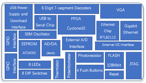
Figure 1 FII-PRA006 system block diagram
(2)FII-PRA006 physical picture
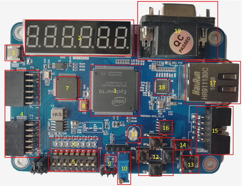
Figure 2 FII-PRA006 physical picture
(3)Corresponding to the physical picture of Figure 2, the main components of the development board are as follows:
1、10CL006YE144C8G or 10CL006YE144C8G
2、6-digit common anode seven-segment display
3、USB power supply and download interface
4、External expansion interface GPIO
5、8 DIP switches
6、8 LEDs
7、USB to serial port chip (FT2232)(Intefrated JTAG download function)
8、50 MHz oscillator
9、Thermistor (NTC-MF52)
10、Potentiometer
11、Photoresistor
12、4 buttons (up, down, right, down)
13、Reset button (Reset)
14、JTAG downloader function conversion interface
15、JTAG download interface (Used only when the board is used as a downloader)
16、Flash (N25Q128A, 128M bit/16M bytes)
17、Ethernet interface
18、Ethernet PHY chip (RTL8211E-VB)
19、VGA interface
20、Back of the board U8: AD/DA conversion chip (PCF8591)
21、Back of the board U13: EEPROM (AT24C02N)
Part Two: FII-PRA006 The Use of Major Hardware Resources and FPGA Development Experiments
This part mainly guides the user to learn the development of the FPGA program and the use of the onboard hardware through the experiment examples of the FPGA. At the same time, the experiment examples are developed from the elementary to the profound to introduction the development system software Quartus II. The experiments covered in this section are as follows.
Experiment 1: LED shifting design experiment
Experiment 2: SignalTap experiment
Experiment 3: Segment display experiment
Experiment 4: Block/SCH experiment
Experiment 5: button debouncing experiment
Experiment 6: use of multiplier and ModelSim simulation
Experiment 7: hex to BCD conversion and application
Experiment 8: usage of ROM
Experiment 9: use dual-ROM to read and write frame data
Experiment 10: asynchrounous serial port design and experiment
Experiment 11: IIC transmission experiment
Experiment 12: AD, DA experiment
Experiment 13: VGA experiment
Experiment 14: Ethernet experiment
Learning exercises in the order of the experimental design, and successfully completing these basic experiments, the level and capabilities of the primary FPGA engineers will be acheived.
- LED shifting, Using Quartus, the Writing of Verilog HDL programs, Mange FPGA Pin Assignment – FPGA Beginner Study Board PRA006, PRA010 Experiment 1
- The Use of SignalTap Logic Analyzer, Analyze the Captured Signals – FPGA Beginner Study Board PRA006, PRA010 Experiment 2
- Use the BCD Code Counter, Digital Display Decoding Design, the Serial Flash, – Segment Display – FPGA Beginner Study Board PRA006, PRA010 Experiment 3
- Building new FPGA Projects in Quartus, Device Selection, PLL setup, PLL Frequency Setting, Verilog’s Tree Hierarchy Design, and the Use of SignalTap II – Block/SCH Experiment – FPGA Beginner Study Board PRA006, PRA010 Experiment 4
- Button Debounce Principle and Adaptive Programming – Button Debounce Experiment – FPGA Beginner Study Board PRA006, PRA010 Experiment 5
- Use ModelSim Simulation to Design Output, Use of Multipliers and ModelSim Simulation – FPGA Beginner Study Board PRA006, PRA010 Experiment 6
- Binary Numbers or Hexadecimal Number to BCD Code Conversion and Application – FPGA Beginner Study Board PRA006, PRA010 Experiment 7
- Study the Format of *.mif File and How to Edit *.mif File ,Study the Internal Memory Block of FPGA,Use of ROM – FPGA Beginner Study Board PRA006, PRA010 Experiment 8
- Configure and Use Dual-port RAM, Use Dual_port RAM to Read and Write Frame Data – FPGA Beginner Study Board PRA006, PRA010 Experiment 9
- Asynchronous Serial Port Communication, Handshake Mechanism and Data Frame Strcuture, Asynchronous Serial Port Design and Experiment – FPGA Beginner Study Board PRA006, PRA010 Experiment 10
- Reading and Writing EEPROM, the Basic Principles of Asynchronous IIC Bus, the IIC Communication Protocol, IIC transmitting Experiment – FPGA Beginner Study Board PRA006, PRA010 Experiment 11
- The knowledge of the IIC protocol, the Theory of AD Conversion, AD, DA Experiment – FPGA Beginner Study Board PRA006, PRA010 Experiment 12
- Design a simple customized VGA image display, Master the principle of VGA implementation, VGA Experiment – FPGA Beginner Study Board PRA006, PRA010 Experiment 13
- Understand What Ethernet is and How it Works, the Relationship Between Different Interface Types (MII, GMII, RGMII) , Ethernet Experiment – FPGA Beginner Study Board PRA006, PRA010 Experiment 14
References
Quartus II Introduction Using VHDL Designs https://www.ee.ryerson.ca/~courses/coe328/Quartus_II_Introduction-V13.pdf
Quartus II Introduction Using VHDL Designs
https://www.ee.ryerson.ca/~courses/coe328/Quartus_II_Introduction-V13.pdf
https://www.nxp.com/docs/en/data-sheet/PCF8591.pdf