Risc-V Board - Digital Clock Comprehensive Design Experiment
Experimental Manuals FPGA Tutor PRX100 Risc-V

Xilinx Risc-V Board Tutorial : Digital Clock Comprehensive Design Experiment- FII-PRX100 FPGA Board Experiment 6

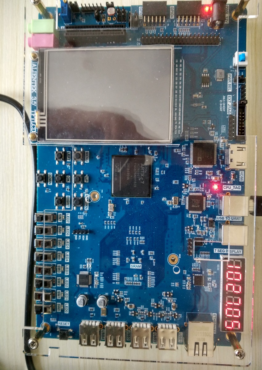
Experiment 6 Digital Clock Comprehensive Design Experiment 1.Experiment Objective Design month, day, hour, minute, and second digital clock experiments, using 6 segment decoders 60 seconds carried to the minute 60 minutes carried to the hour 24 hours carried to the day 30 days carried to the month, and reset all Set four keys: menu, left, up, down The menu key controls the calibration function to switch between clock, date, and alarm. The left key selects which value is currently calibrated The Up and down keys add 1 and subtract 1…

Read More
Button Debounce Design and Experimental-
Experimental Manuals FPGA Tutor PRX100 Risc-V

Xilinx Risc-V Board Tutorial : Button Debounce Design and Experimental- FII-PRX100 FPGA Board Experiment 5

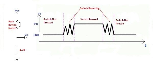
Experiment 5 Button Debounce Design and Experimental 1.Experiment Objective Review the design of blinking LED Learn the principle of button debounce, and adaptive programming Learn the connection and use of the FII-PRX100T button schematics Integrated application of button debounce and another compatible program design 2.Experiment Button debounce principle Usually, the switches used for the buttons are mechanical elastic switches. When the mechanical contacts are opened and closed, due to the elastic action of the mechanical contacts, a push button switch does not immediately turn on when closed, nor is it…

Read More
JTAG Configuration Description - FII-PRA010
Configuration Pocket Boards

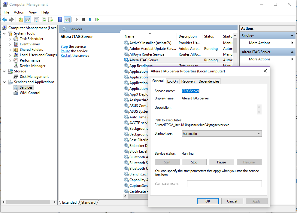
JTAG Configuration Description – FII-PRA010 – Cyclone-10 FPGA Development Board with Jtag Embeded

FII-PRA010 – Cyclone-10 FPGA Development Board is based on our FII-PRA010 fpga board. You can buy it only $59. The official shopping website: https://fpgamarketing.com/FPGA-Study-Board-Verilog-for-beginner-Cyclone-10-FII-PRA006-FII-PRA006.htm Altera FPGA Study Board, Verilog for beginner – Cyclone-10 FPGA Development Board with Jtag Embeded – FII-PRA006 The advantage of FPGA beginner board: Beginner FPGA study board, cheaper but fully functional. cellphone sized. ( < 100 USD ) power supply and download at the same time, no extra power supply and no extra data transfer line needed Small volume and light and can be put into…

Read More
JTAG Configuration Description - FII-PRA006
Configuration Pocket Boards

JTAG Configuration Description – FII-PRA006 – Cyclone-10 FPGA Development Board with Jtag Embeded

The latest DLL versions for Altera Quartus II or Intel Quartus Prime are 1.8b (Provided in the folder), for Quartus in Linux, get version 1.7b. To install the driver for Quartus II, do the following: Connect the MBFTDI programmer with a USB cable to a Windows computer. Make sure the device is detected and the FTDI drivers are already installed. To do this, look in the Device Manager Windows, in the COM and LPT ports section, two COM ports should appear. If instead you find two yellow question marks, then you need…

Read More
Block/SCH Digital Clock Design
Experimental Manuals FPGA Tutor PRX100 Risc-V

Xilinx Risc-V Board Tutorial : Block/SCH Digital Clock Design- FII-PRX100 FPGA Board Experiment 4

Experiment 4 Block/SCH Digital Clock Design 1.Experiment Objective Review the new FPGA project building in Vivado, device selection, PLL creation, PLL frequency setting, Verilog tree hierarchy design, and the use of ILA Master the design method of graphics from top to bottom Combine the BCD_counter project to realize the movement of the decimal point (DP) of the decoder Observe the test result 2.Experiment Procedure File -> Project -> New Project Name:block_counter Select Device: XC7A100T-2FGG676I See Fig 4. 1, add source file, new top-level entity: block_counter.v Fig 4. 1 Build source…

Read More
isc-V Board Tutorial : Basic Digital Clock Experiment and Programming of FPGA Configuration Files
Experimental Manuals FPGA Tutor PRX100 Risc-V

Xilinx Risc-V Board Tutorial : Basic Digital Clock Experiment and Programming of FPGA Configuration Files- FII-PRX100 FPGA Board Experiment 3

Experiment 3 Basic Digital Clock Experiment and Programming of FPGA Configuration Files 1.Experiment Objective Review the contents of experiment 1 and experiment 2, master the configuration of PLL, the design of frequency divider, the principle of schematics and the pin assignment of FPGA. Study BCD decoder Display design of 4-digit hexadecimal to 7 segment display decoders Generate a programmable configuration file and program it to the serial FLASH of the development board through the JTAG interface. 2.Design of The Experiment Refer experiment 1 for building new projects, chip selection module…

Read More
Altera Risc-V fpga board
Experimental Manuals FPGA Tutor PRX100 Risc-V

Xilinx Risc-V Board Tutorial : Switches and Display – FII-PRX100 FPGA Board Experiment 2

Experiment 2 Switches and display 1.Experiment Objective Continue to practice using develop board Learn to use ILA (Integrated Logic Analyzer) in Vivado Learn to use the FPGA configuration memory for programming 2.Start New Project Refer to Experiment 1 Select the same chip in Experiment 1 Add PLL1 (Here PLL1 is optional, external input clock can be used directly) 3.Verilog HDL Code module SW_LED( input inclk, input [7:0] sw, output reg[7:0] led ); wire sys_clk; wire pll_locked; reg sys_rst; always@(posedge sys_clk) sys_rst<=!pll_locked;   always @(posedge inclk) if(sys_rst) led<=8’hff; else led<=~sw; PLL1…

Read More
Experimental Manuals FPGA Tutor PRX100 Risc-V

Verilog HDL program to achieve frequency division, Write Verilog HDL program to implement LED shifting – Risc-V FPGA Board Xilinx – Development Board Experiment 1 – LED Shifting – FII-PRX100

Experiment 1 LED Shifting 1. Experiment Object Practice how to use the development system software Vivado to establish a new project, call the system resource PLL to establish the clock. Write Verilog HDL program to achieve frequency division Write Verilog HDL program to implement LED shifting Combine hardware resources for FPGA pin configuration Compile Download the program to the develop board Observe the experimental result and debug the project 2. Create A New Project Under Vivado Start Vivado in the start Menu. See Fig 1. 1 Fig 1. 1 Start…

Read More
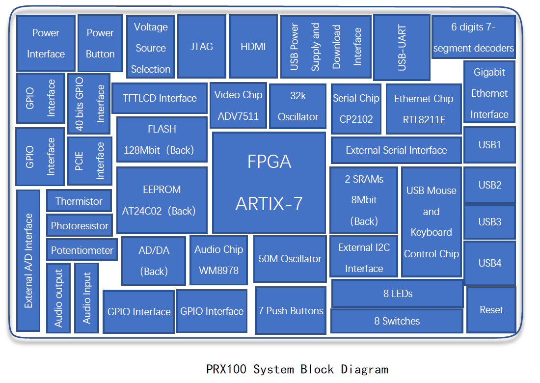
prx100 system block diagram
Experimental Manuals FPGA Tutor PRX100 Risc-V

xilinx Risc-V FPGA Board – FII-PRX100 – FPGA Development Board System Introduction

  FII-PRX100 Development Board ( ARTIX 100T, XC7A100T, RISC-V FPGA Developing Board) Online Shopping: https://fpgamarketing.com/FII-PRX100-ARTIX-100T-XC7A100T-RISC-V-FPGA-Board-PRX100-1.htm Fraser Innovation Inc develops FII-PRX100 based on the boards of the Xilinx ARTIX-7 series. It was initial released in 2018. This development board is resource-rich and high-speed, making it an ideal platform for learning and engineering research. This development board has been spent a lot on system design, PCB design, and function creation. It could even be said comprehensive and powerful. System Design Objective The main purpose of this system design is to complete FPGA learning,…

Read More
FPGA for Beginners Hardware Reference Guide

FPGA Board for beginner – FII-PRA006/010 Hardware Reference Guide

V1.2 FII-PRA006/010 Hardware Reference Guide Version Control Version Date Description V1.0 06/25/2019 Initial Release V1.1 07/15/2019 Add Description About PCF8591 V1.2 07/19/2019 Add Description About Oscillator and IIC Copyright Notice: © 2019 Fraser Innovation Inc ALL RIGHTS RESERVED Without written permission of Fraser Innovation Inc, no unit or individual may extract or modify part of or all the contents of this manual. Offenders will be held liable for their legal responsibility. Thank you for purchasing the FPGA development board. Please read the manual carefully before using the product and make…

Read More