FPGA Board Based FPGA for Beginners FPGA Tutor Pocket Boards PRA006/PRA010

Reading and Writing EEPROM, the Basic Principles of Asynchronous IIC Bus, the IIC Communication Protocol, IIC transmitting Experiment – FPGA Beginner Study Board PRA006, PRA010 Experiment 11

Experiment 11 IIC transmitting Experiment 11.1 Experiment Objective Learning the basic principles of asynchronous IIC bus, and the IIC communication protocol Master the method of reading and writing EEPROM Joint debugging using logic analyzer 11.2 Experiment Implement Correctly write a number to any address in the EEPROM (this experiment writes to the register of 8’h03 address) through the FPGA (here changes the written 8-bit data value by (SW7~SW0)). After writing in successfully, read the data as well. The read data is displayed directly on the segment display. Program the FPGA…

Read More
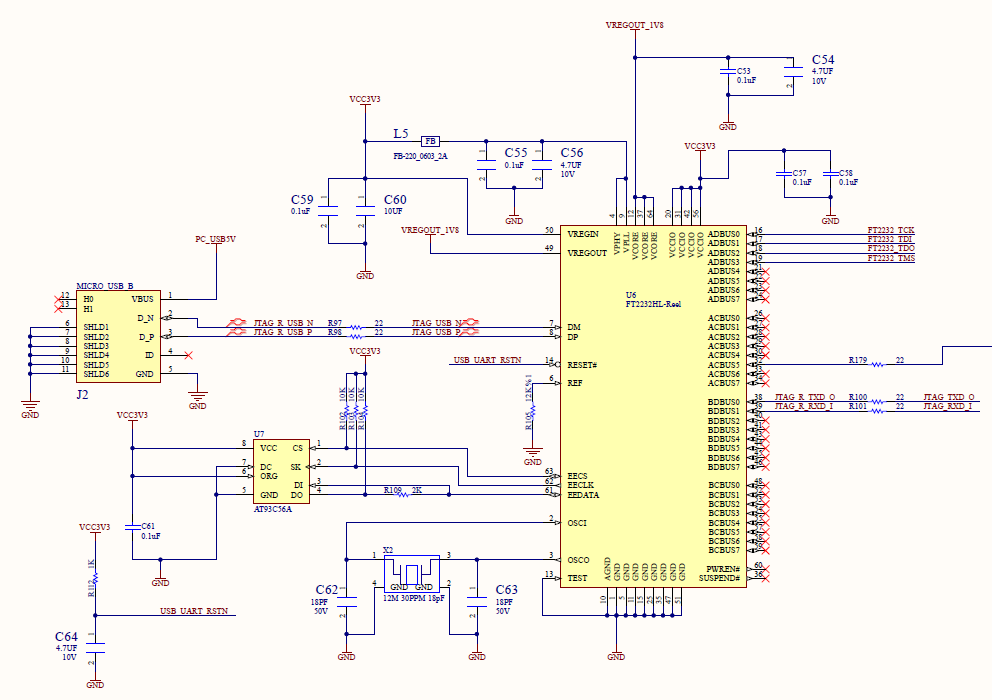
scheme of series ports
Experimental Manuals FPGA for Beginners Pocket Boards PRA006/PRA010

Asynchronous Serial Port Communication, Handshake Mechanism and Data Frame Strcuture, Asynchronous Serial Port Design and Experiment – FPGA Beginner Study Board PRA006, PRA010 Experiment 10

Experiment 10 Asynchronous Serial Port Design and Experiment 10.1 Experiment Objective Because asynchronous serial ports are very common in industrial control, communication, and software debugging, they are also vital in FPGA development. Study the basic principles of asynchronous serial port communication, handshake mechanism and data frame strcuture Master asynchronous sampling techniques Review the frame structure of the data packet Learn to use FIFO Joint debugging with common debugging software of PC (SSCOM, Tera Term, etc.) 10.2 Experiment Implement Design and transmit full-duplex asynchronous communication interface Tx, Rx Baud rate of…

Read More
Experimental Manuals FPGA for Beginners FPGA Tutor Pocket Boards PRA006/PRA010

Configure and Use Dual-port RAM, Use Dual_port RAM to Read and Write Frame Data – FPGA Beginner Study Board PRA006, PRA010 Experiment 9

Experiment 9 Use Dual_port RAM to Read and Write Frame Data 9.1 Experiment Objective Learn to configure and use dual-port RAM Learn to use synchronous clock to control the synchronization of frame structure Learn to use asynchronous clock to control the synchronization of frame structure Experiment Implement Observing the synchronization structure of synchronous clock frames using SignalTap II Extended the use of dual-port RAM Design the use of three-stage state machine Design a 16-bit data frame Data is generated by an 8-bit counter: Data={~counta,counta} The ID of the data frame…

Read More
Experimental Manuals FPGA for Beginners FPGA Tutor Pocket Boards PRA006/PRA010

Study the Format of *.mif File and How to Edit *.mif File ,Study the Internal Memory Block of FPGA,Use of ROM – FPGA Beginner Study Board PRA006, PRA010 Experiment 8

Experiment 8 Use of ROM 8.1 Experiment Objective Study the internal memory block of FPGA Study the format of *.mif and how to edit *.mif file to configure the contents of ROM Learn to use RAM, read and write RAM 8.2 Experiment Implement Design 16 outputs ROM, address ranging 0-255 Interface 8-bit switch input as ROM’s address Segment display illustrates the contents of ROM and require conversion of hexadecimal to BCD output. 8.3 Experiment 8.3.1 Introduction to Program This experiment was carried out on the basis of Experiment 7, and…

Read More
Experimental Manuals FPGA Board Based FPGA for Beginners PRA006/PRA010

Binary Numbers or Hexadecimal Number to BCD Code Conversion and Application – FPGA Beginner Study Board PRA006, PRA010 Experiment 7

Experiment 7 Hexadecimal Number to BCD Code Conversion and Application Experiment Objective Learn to convert binary numbers to BCD code (bin_to_bcd) Learn to convert hexadecimal numbers to BCD code (hex_to_bcd) 7.2 Experiment Implement Combined with experiment 6, display the results of the operation to the segment display. 7.3 Experiment 7.2.1 Introduction to the Principle of Converting Hexadecimal Number to BCD Code Since the hexadecimal display is not intuitive, decimal display is more widely used in real life. Human eyes recognition is relatively slow, so the display from hexadecimal to decimal…

Read More
Experimental Manuals FPGA for Beginners FPGA Tutor PRA006/PRA010

Use ModelSim Simulation to Design Output, Use of Multipliers and ModelSim Simulation – FPGA Beginner Study Board PRA006, PRA010 Experiment 6

Experiment 6 Use of Multipliers and ModelSim Simulation 6.1 Experiment Objective Learn to use multiplier Use ModelSim simulation to design output 6.2 Experiment Implement 8×8 multiplier, the first input value is an 8-bit switch, and the second input value is the output of an 8-bit counter. Observe the output in ModelSim Oberseve the calculation results with a four-digit segment display 6.3 Experiment Since the simulation tools and the new IP core are used here, there is no introduction or design part of hardware. 6.3.1 Introduction of Program ModelSim is an…

Read More
Experimental Manuals FPGA Board Based FPGA for Beginners FPGA Tutor PRA006/PRA010

Button Debounce Principle and Adaptive Programming – Button Debounce Experiment – FPGA Beginner Study Board PRA006, PRA010 Experiment 5

Experiment 5 Button Debounce Experiment 5.1 Experiment Objective Review the design process of the shifting LED Learn button debounce principle and adaptive programming Study the connection and use of the FII-PRA006/010 button hardware circuit Comprehensive application button debounce and other conforming programming 5.2 Experiment Implement Control the movement of the lit LED by pressing the button Each time the button is pressed, the lit LED moves one bit. When the left shift button is pressed, the lit LED moves to the left, presses the right button, and the lit LED…

Read More
Experimental Manuals FPGA Board Based FPGA for Beginners PRA006/PRA010

Building new FPGA Projects in Quartus, Device Selection, PLL setup, PLL Frequency Setting, Verilog’s Tree Hierarchy Design, and the Use of SignalTap II – Block/SCH Experiment – FPGA Beginner Study Board PRA006, PRA010 Experiment 4

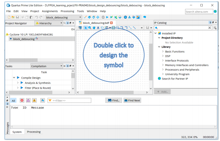
Experiment 4 Block/SCH Experiment 4.1 Experiment Objective Review building new FPGA projects in Quartus, device selection, PLL setup, PLL frequency setting, Verilog’s tree hierarchy design, and the use of SignalTap II Master the design method of graphics from top to bottom Combined with the BCD_counter project to achieve the display of the digital clock Observe the experimental results 4.2 Experiment Implement Use schematics design to build the project 4.3 Experiment This experiment is mainly to master another design method. The other design contents are basically the same as the experiment…

Read More
Experimental Manuals FPGA Board Based FPGA for Beginners FPGA Tutor PRA006/PRA010

Use the BCD Code Counter, Digital Display Decoding Design, the Serial Flash, – Segment Display – FPGA Beginner Study Board PRA006, PRA010 Experiment 3

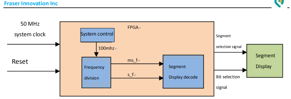
Experiment 3 Segment Display 3.1 Experiment Objective Review previous experiments, proficient practice in PLL configuration, frequency division design, and project verification; Learn to use the BCD code counter; Digital display decoding design; Learn to program the project into the serial FLASH of the development board; 3.2 Experiment Implement The segment display has two lower (right most) digits to display seconds, the middle two digits to display minutes, and the highest (left most) two digits to display hours. The decimal point remains off and will not be considered for the time…

Read More
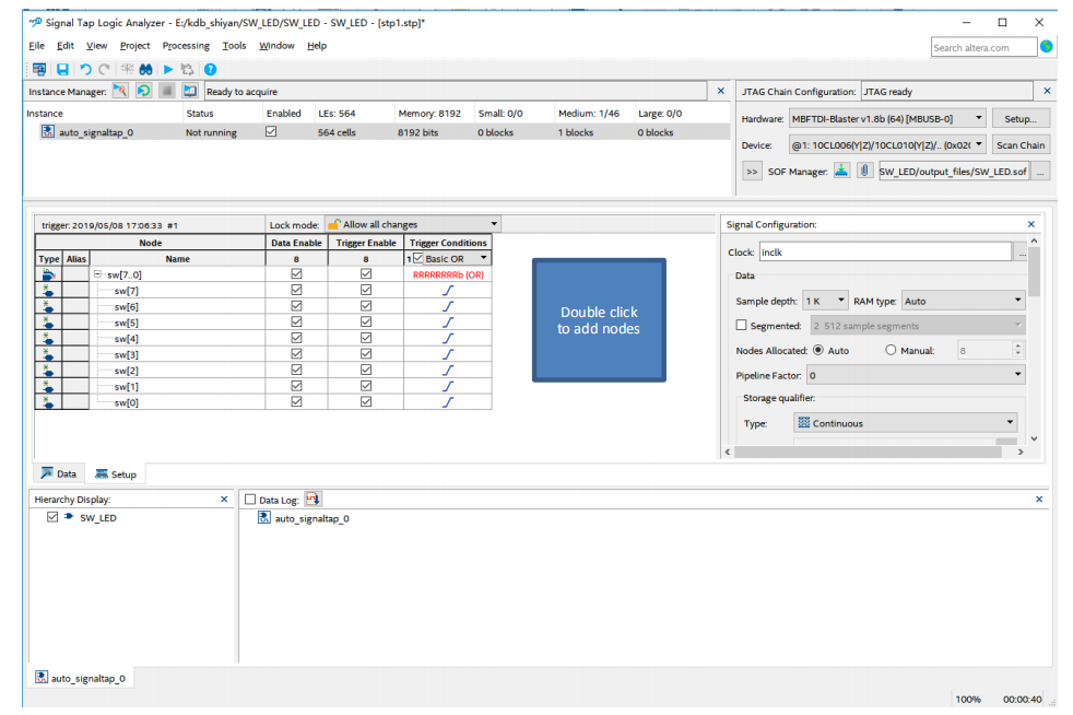
Signal Tap setting
Experimental Manuals FPGA Board Based FPGA for Beginners FPGA Tutor PRA006/PRA010

The Use of SignalTap Logic Analyzer, Analyze the Captured Signals – FPGA Beginner Study Board PRA006, PRA010 Experiment 2

Experiment 2 SignalTap 2.1 Experiment Objective Continue to practice using of the development board hardware; Practice the use of SignalTap Logic Analyzer in Quartus; Learn to analyze the captured signals. 2.2 Experiment Implement Capture and analyze the switching signals on the development board through the use of SignalTap. 2.3 Experiment 2.3.1 Introduction to the Switches and SignalTap Introduction to the switches The on-board switch is 8 DIP switches, as shown in Figure 2.1. The switch is used to switch the circuit by turning the switch handle using the binary coding…

Read More