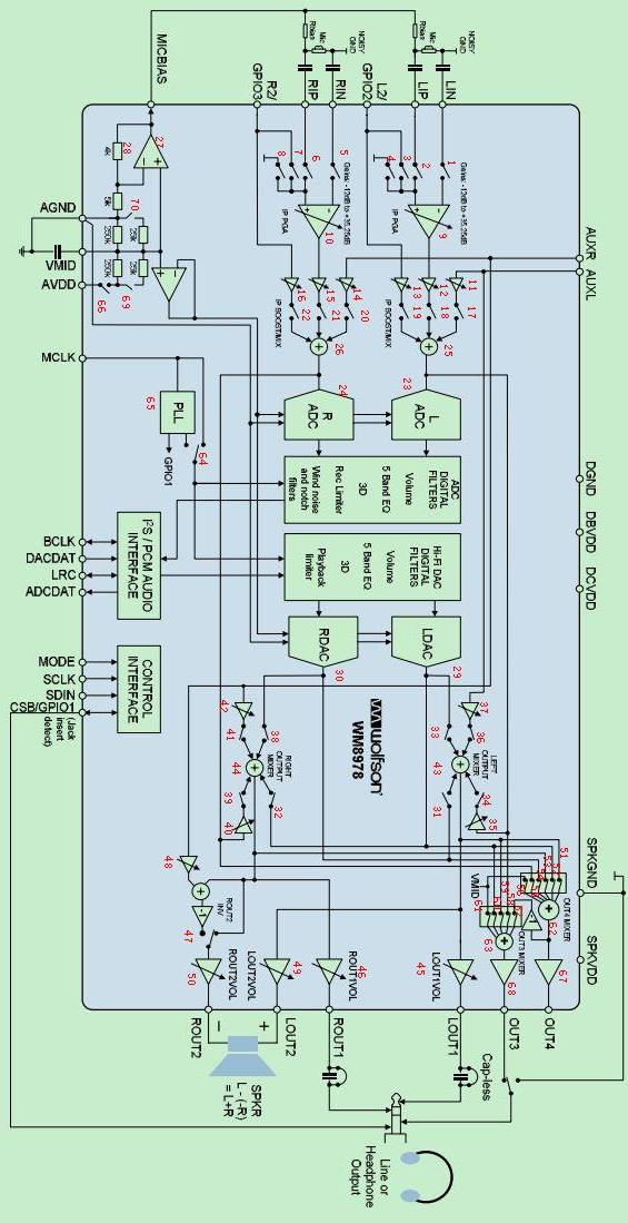
WM8978 internal structure block diagram
Experimental Manuals FII-PRA040 FPGA Board Based FPGA Tutor Risc-V

Audio 8978 Loopback Experiment (WM8978 Audio Sub Development Board) , How I2S (Inter-IC Sound) bus work ? – – FII-PRA040 Altera Risc-V Tutorial Experiment 16

Experiment 16 8978 Audio Loopback Experiment 16.1 Experiment Objective Learn about I2S (Inter-IC Sound) bus and how it works Familiar with the working mode of WM8978. And by configuring the interface mode and selecting the relevant registers in combination with the development board, complete the data transmission and reception, and verify it 16.2 Experiment Implement Perform audio loopback test by configuring the onboard audio chip WM8978 to check if the hardware is working properly Adjust the volume output level with the keys. 16.3 Experiment 16.3.1 WM8978 Introduction WM8978 is a…

Read More
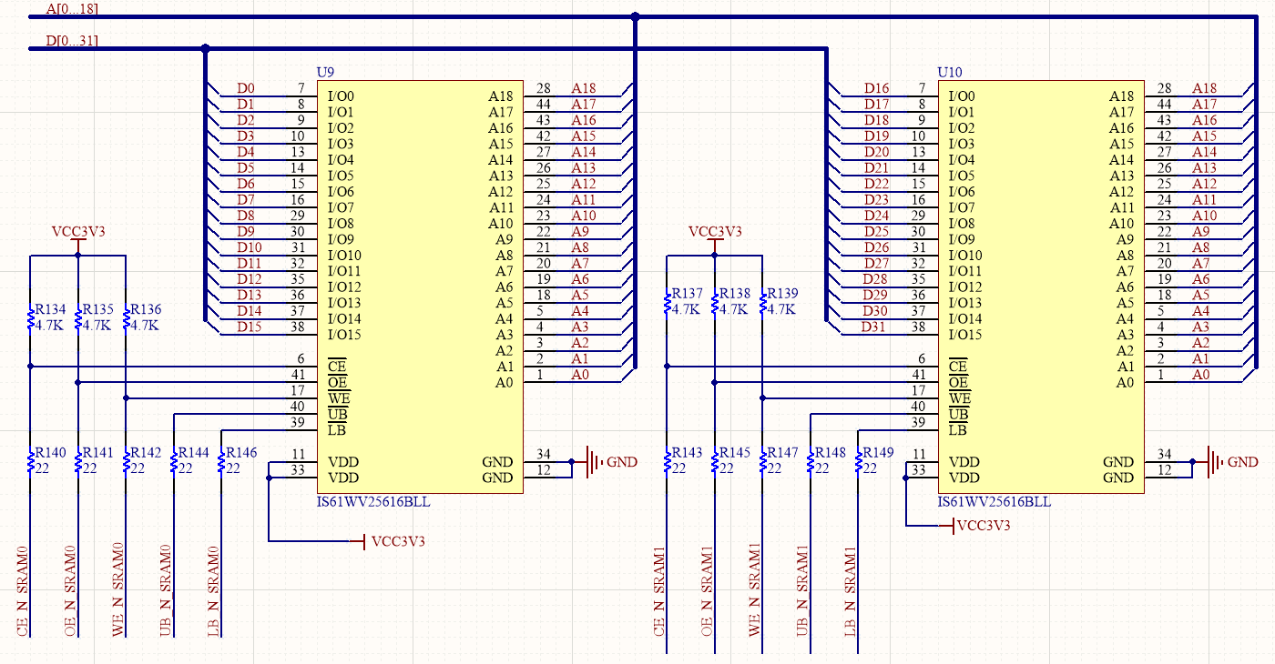
chematics of SRAM
FII-PRA040 FPGA Board Based FPGA Tutor Risc-V

How does SRAM read and write work ? Review frequency division, button debounce, and hex conversion experiment – FII-PRA040 Altera Risc-V Tutorial Experiment 15

Experiment 15 SRAM Read and Write 15.1 Experiment Objective Learn the read and write of SRAM Review frequency division, button debounce, and hex conversion experiment content 15.2 Experiment Implement Control the read and write function of SRAM by controlling the button The data written to the SRAM is read out again and displayed on the segment display In the process of reading data, it is required to have a certain time interval for each read operation. 15.3 Experiment 15.3.1 Introduction to SRAM SRAM (Static Random-Access Memory) is a type of…

Read More
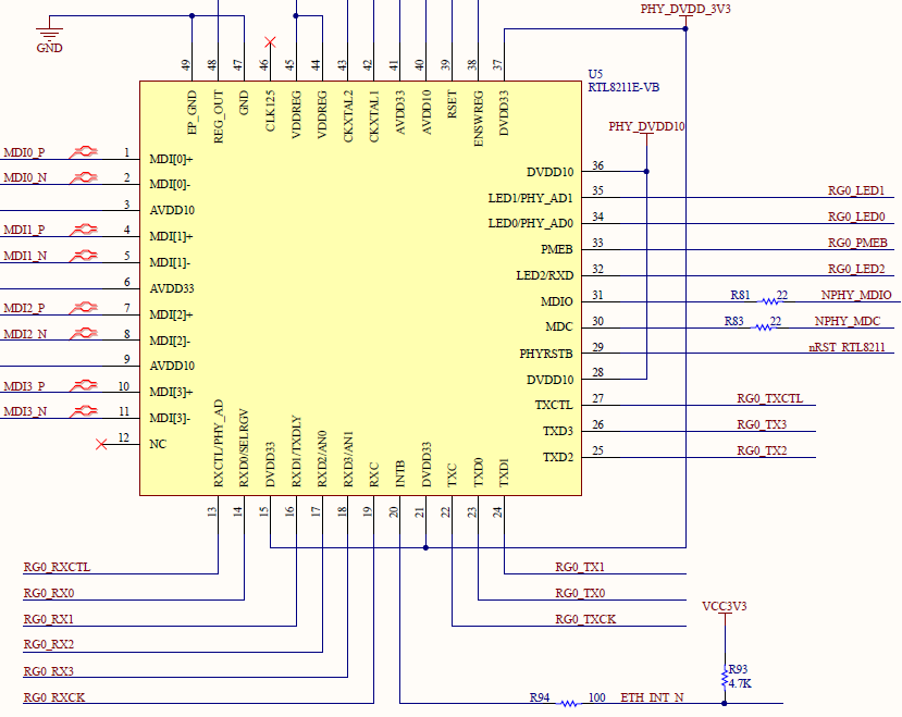
Schematics of RTL8211E-VB
FII-PRA040 FPGA Board Based FPGA Tutor Risc-V

How does Ethernet work? MII, GMII, RGMII interface advantages and disadvantages, Perform a loopback test, FII-PRA040 Altera Risc-V Tutorial Experiment 14

Experiment 14 Ethernet 14.1 Experiment Objective Understand what Ethernet is and how it works Familiar with the relationship between different interface types (MII, GMII, RGMII) and their advantages and disadvantages (FII-PRA040 uses RGMII) Combine the development board to complete the transmission and reception of data and verify it 14.2 Experiment Implement Perform a loopback test to check if the hardware is working properly. Perform data receiving verification Perform data transmission verification 14.3 Experiment 14.3.1 Introduction to Experiment Principle Ethernet is a baseband LAN technology. Ethernet communication is a communication method…

Read More
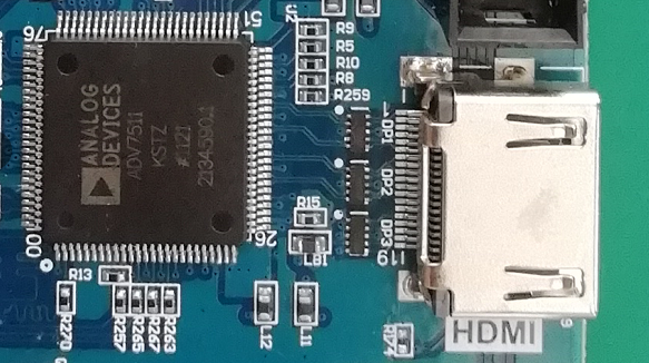
HDMI interface and ADV7511 chip physical photo
Experimental Manuals FII-PRA040 FPGA Board Based FPGA Tutor Risc-V

Learn HDMI principle, Introduction to HDMI and ADV7511 Chip, HDMI Display, FII-PRA040 Altera Risc-V tutorial Experiment 13

Experiment 13 HDMI Display 13.1 Experiment Objective Review IIC protocol Review EEPROM read and write Learn HDMI principle 13.2 Experiment Implement Display different image content on the screen through the HDMI. 13.3 Experiment 13.3.1 Introduction to HDMI and ADV7511 Chip Image display processing has always been the focus of FPGA research. At present, the image display mode is also developing. The image display interface is also gradually transitioning from the old VGA interface to the new DVI or HDMI interface. HDMI (High Definition Multimedia Interface) is a digital video/audio interface…

Read More
FII-PRA040

FII-PRA040 User Experimental Manuals ( 2020-09-28 Updated )

  PRA040 USER EXPERIMENTAL MANUAL PRA040 EXPERIMENTAL INSTRUCTIONS FRASER INNOVATION INC December 07, 2019 Version Control Version Date Description 1.0 07/20/2019 Initial Release 1.1 07/29/2019 Add Experiment 15 1.2 07/31/2019 Revised some description about HDMI 1.3 08/16/2019 SRAM part revised 1.4 08/30/2019 Add a description in Ethernet 1.5 09/17/2019 Revise some syntax and code error 1.6 12/06/2019 Add Experiments 16-19 Contents Project Files Appendix 9 Part One: Introduction of FII-PRA040 Development System 10 1、Design Objective of the System 10 2、System Resource 10 3、Human-computer Interaction Interface 10 4、Software Development System 11…

Read More
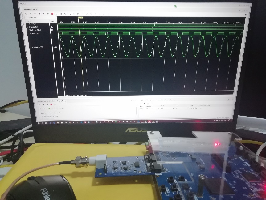
Signal waveform of AD9226 captured by logic analyzer
FII-PRX100-S FII-PRX100D PRX100

FII-PRX100T User Experiment Manuals (newly updated 2020-09-28)

  PRX100 USER experimental manual PRX100 EXPERIMENTAL INSTRUCTIONS FRASER INNOVATION INC December 11, 2019 Version Control Version Date Descrption V1.0 07/10/2019 Initial Release V1.1 09/16/2019 Modify part of pin assignments and Ethernet description V1.2 12/12/2019 Add Experiments 15-20 Contents: Part 1 FII-PRX100 Development System Introduction 6 1. System Design Objective 6 2. System Resource 6 3. Human-computer Interaction Interface 6 4. Software Development System 7 5. Supporting Resources 7 Part 2 FII-PRX100 Main Hardware Resources Usage and FPGA Development Experiment 7 Experiment 1 LED Shifting 7 1. Experiment Object 7…

Read More
https://fraserinnovations.com/wp-content/uploads/2018/09/ad9361-front.png
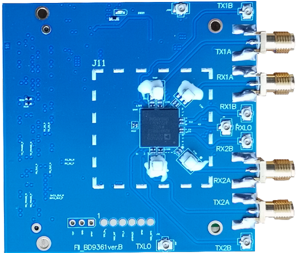
FII-BD9361 RF Transceivers

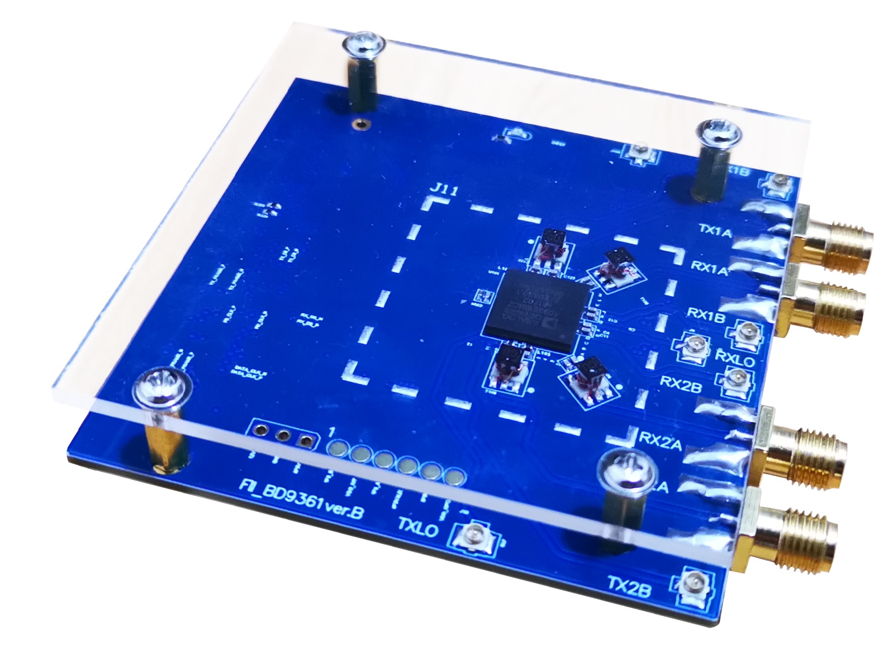
FII-BD9361 (AD-FMCOMMS3-EBZ Board Compatible) Hardware Configuration

V1.0 Fraser innovation inc FII-BD9361 Hardware Reference Guide Version Control Version Date Description V1.0 12/03/2019 Initial Release Copyright Notice: © 2019 Fraser Innovation Inc ALL RIGHTS RESERVED Without written permission of Fraser Innovation Inc, no unit or individual may extract or modify part of or all the contents of this manual. Offenders will be held liable for their legal responsibility. Thank you for purchasing the FPGA development board. Please read the manual carefully before using the product and make sure that you know how to use the product correctly. Improper…

Read More
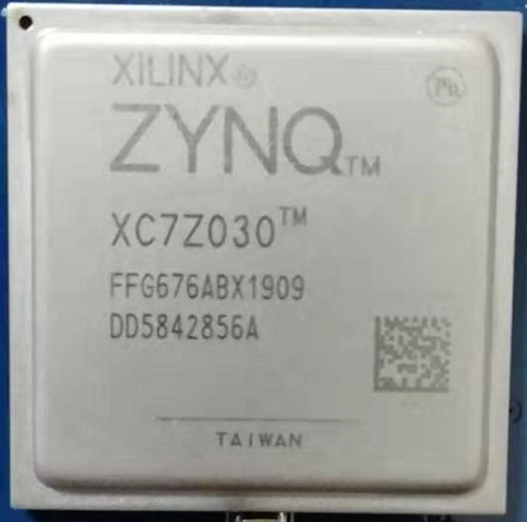
Xilinx ZYNQ XC7Z030
Configuration FII-PE7030

xc7z030 board hardware resources and block diagram of ZYNQ chip

This development board uses Xilinx’s zynq7000 series chip, model XC7Z030-2FFG676I, 676-pin FPGA package. This chip can be divided into a PS (Processor System) part and a PL (Programmable Logic) part. On the PE7030 development board, the PS and PL sections of the XC7Z030 are both equipped with a wealth of external interfaces and devices for convenience use and functional verification. In addition, as always, the USB Cable downloader circuit is integrated on the development board. Users only need to use a USB cable to download and debug the development board.…

Read More
FII-PRA006-physical-picture
FPGA for Beginners

What is the main components of the FRA006 FPGA beginner board with JTAG downloader ?

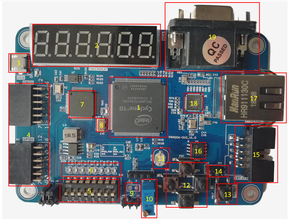
What is the main components of the FRA006 FPGA beginner board ? What is the main components of the FRA006 FPGA beginner board ? 10CL006YE144C8G or 10CL006YE144C8G 6-digit common anode seven-segment display USB power supply and download interface External expansion interface GPIO 8 DIP switches 8 LEDs USB to serial port chip (FT2232)(Intefrated JTAG download function) 50 MHz oscillator Thermistor (NTC-MF52) Potentiometer Photoresistor 4 buttons (up, down, right, down) Reset button (Reset) JTAG downloader function conversion interface JTAG download interface (Used only when the board is used as a downloader)…

Read More
AD-FMCOMMS3-EBZ
FPGA Board Based RF Transceivers USRP

What is the features and benefits of your FII-BD9361 (AD-FMCOMMS3-EBZ compatible ) boards ?

What is the FII-BD9361 Features: We support all features of AD-FMCOMMS3-EBZ such as: TX band: 47 MHz to 6.0 GHz RX band: 70 MHz to 6.0 GHz Bandwidth Adjustment Range: 200 kHz to 56 MHz Low noise figure: 2dB NF(noise figure/800MHz ) LO ,RX Gain Control,AGC 2.4Hhz local oscillator (LO) step For more information, please check ad9361 introduction. What is the benefits of AD-FMCOMMS3-EBZ ( Compatible with FII-BD9361) Software tunable across wide frequency range : TX :47 MHz to 6 GHz RX:70 MHz to 6 GHz Software tunable bandwidth: 200…

Read More