Sawtooth wave
Experimental Manuals FII-PRX100-S FII-PRX100D FPGA Board Based FPGA Tutor PRX100 Risc-V

DAC9767 DDS Signal Source Experiment – Xilinx Risc-V Board FII-PRX100 Experiment 20

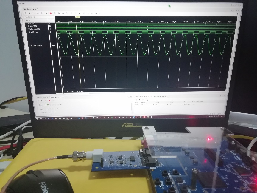
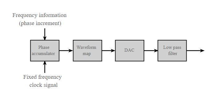
Experiment 20 DAC9767 DDS Signal Source Experiment 20.1 Experiment Objective Learn about DDS (Direct Digital Synthesizer) related theoretical knowledge. Read the AD9767 datasheet and use the AD9767 to design a signal source that can generate sine, square, triangle, and sawtooth waves. 20.2 Experiment Implement Learn about DDS theoretical knowledge. On the basis of understanding the principle of DDS, combined with the theoretical knowledge, use AD9767 module and development board to build a signal source whose waveform, amplitude and frequency can be adjusted. (There are no specific requirements for the adjustment…

Read More
Signal waveform of AD9226 captured by logic analyzer
Experimental Manuals FII-PRX100-S FII-PRX100D FPGA Board Based FPGA Tutor PRX100 Risc-V

High-speed ADC9226 Acquisition Experiment – Xilinx Risc-V Board FII-PRX100 Experiment 19

Experiment 19 High-speed ADC9226 Acquisition Experiment 19.1 Experiment Objective Learn about parallel ADC collectors and master the use of ADC9226. 19.2 Experiment Implement 1. Insert the ADC9226 module face up into the FPGA development board to the GPIO2 and GPIO1 ports which are next to the red-green audio module. Write programs to use this module to test 19.3 Experiment 19.3.1 ADC9226 Module Introduction ADC9226 module adopts AD9226 chip design of ADI Company. This chip is a monolithic, 12-bit, 65 MSPS analog-to-digital converter (ADC). It uses a single power supply and…

Read More
5640 display shows taken picture
Experimental Manuals FII-PRX100-S FII-PRX100D FPGA Board Based PRX100 Risc-V

Photo Display Experiment of OV5640 Camera , Understand the power-on sequence of the OV5640 camera and the corresponding register configuration process – Xilinx Risc-V Board FII-PRX100 Experiment 18

Experiment 18 Photo Display Experiment of OV5640 Camera 18.1 Experiment Objective Understand the power-on sequence of the OV5640 camera and the corresponding register configuration process when outputting images of different resolutions Review previous knowledge of IIC bus Review previous knowledge of HDMI 18.2 Experiment Implement Read the power-on sequence of the OV5640 datasheet, and correctly write the power-on control program according to the peripheral module schematics. Correctly write the configuration program of the OV5640 camera with a resolution of 640X480 according to the timing requirements of the SCCB interface Based…

Read More
SRAM read timing
Experimental Manuals FII-PRX100-S FII-PRX100D FPGA Board Based PRX100 Risc-V

Reading Experiment of Serial Port Partition of Static Memory SRAM, Read and write timing of IS61WV25616BLL SRAM, and prepare for the next experimental experiment of OV5640 camera experiment – – Xilinx Risc-V FII-PRX100 Board Experiment 17

Experiment 17 Reading Experiment of Serial Port Partition of Static Memory SRAM 17.1 Experiment Objective Learn about static memory SRAM read and write operations and how it works Familiar with the read and write timing of IS61WV25616BLL SRAM, and prepare for the next experimental experiment of OV5640 camera experiment. 17.2 Experiment Implement The experimental board is equipped with two pieces of SRAM, which are combined to form 18-bit address lines and 32-bit data spaces. After power-on, the FPGA will write the same value in the corresponding address in the entire…

Read More
Schematics of RTL8211E-VB
Experimental Manuals FII-PRX100-S FII-PRX100D FPGA Board Based FPGA Tutor PRX100 Risc-V

How ethernet work and familiar with MII, GMII, RGMII interface types – FII-PRX100 Risc-V Board Experiment 15

Experiment 15 Ethernet 15.1 Experiment Objective Understand what Ethernet is and how it works Familiar with the relationship between different interface types (MII, GMII, RGMII) and their advantages and disadvantages (FII-PRA040 uses RGMII) Combine the development board to complete the transmission and reception of data and verify it 15.2 Experiment Implement Perform a loopback test to check if the hardware is working properly. Perform data receiving verification Perform data transmission verification 15.3 Experiment 15.3.1 Introduction to Experiment Principle Ethernet is a baseband LAN technology. Ethernet communication is a communication method…

Read More
Test case for jal instruction
Experimental Manuals FII-PRA040 FII-PRX100-S FII-PRX100D Hardware Reference Guide Risc-V Risc-V Tutorial

ASM Test Introduction

  V1.0 Fraser Innovation inc asm_test introduction document Version Control Version Date Description 1.0 09/29/2020 Initial Release Copyright Notice: © 2020 Fraser Innovation Inc ALL RIGHTS RESERVED Without written permission of Fraser Innovation Inc, no unit or individual may extract or modify part of or all the contents of this manual. Offenders will be held liable for their legal responsibility. Thank you for purchasing the FPGA development board. Please read the manual carefully before using the product and make sure that you know how to use the product correctly. Improper…

Read More
DDS block diagram
Experimental Manuals FII-PRA040 Risc-V

DAC9767 DDS Signal Source Experiment, AD9767 datasheet and use the AD9767 to design a signal source that can generate sine, square, triangle, and sawtooth waves – FII-PRA040 Altera Risc-V Experiment 19

Experiment 19 DAC9767 DDS Signal Source Experiment 19.1 Experiment Objective Learn about DDS (Direct Digital Synthesizer) related theoretical knowledge. Read the AD9767 datasheet and use the AD9767 to design a signal source that can generate sine, square, triangle, and sawtooth waves. 19.2 Experiment Implement Learn about DDS theoretical knowledge. On the basis of understanding the principle of DDS, combined with the theoretical knowledge, use AD9767 module and development board to build a signal source whose waveform, amplitude and frequency can be adjusted. (There are no specific requirements for the adjustment…

Read More
ADC9226 timing diagram
Experimental Manuals FII-PRA040 FPGA Board Based FPGA Tutor Risc-V

High-speed ADC9226 Acquisition Experiment (FII-BD9226) – parallel ADC collectors and master the use of ADC9226 – FII-PRA040 Altera Risc-V Experiment 18

  Experiment 18 High-speed ADC9226 Acquisition Experiment 18.1 Experiment Objective Learn about parallel ADC collectors and master the use of ADC9226. 18.2 Experiment Implement Insert the ADC9226 module face up into the FPGA development board to the GPIO2 and GPIO1 ports which are next to the red-green audio module. Write programs to use this module to test 18.3 Experiment 18.3.1 ADC9226 Module Introduction ADC9226 module adopts AD9226 chip design of ADI Company. This chip is a monolithic, 12-bit, 65 MSPS analog-to-digital converter (ADC). It uses a single power supply and…

Read More
5640 power-on sequence
Experimental Manuals FII-PRA040 FPGA Board Based FPGA Tutor Risc-V

OV5640 Camera Photo Display Experiment, IIC bus, HDMI, Understand the power-on sequence of the OV5640 – FII-PRA040 Altera Risc-V Experiment 17

Experiment 17 Photo Display Experiment of OV5640 Camera 17.1 Experiment Objective Understand the power-on sequence of the OV5640 camera and the corresponding register configuration process when outputting images of different resolutions Review previous knowledge of IIC bus Review previous knowledge of HDMI 17.2 Experiment Implement Read the power-on sequence of the OV5640 datasheet, and correctly write the power-on control program according to the peripheral module schematics. Correctly write the configuration program of the OV5640 camera with a resolution of 640X480 according to the timing requirements of the SCCB interface Based…

Read More