ADC9226 timing diagram
Experimental Manuals FII-PRA040 FPGA Board Based FPGA Tutor Risc-V

High-speed ADC9226 Acquisition Experiment (FII-BD9226) – parallel ADC collectors and master the use of ADC9226 – FII-PRA040 Altera Risc-V Experiment 18

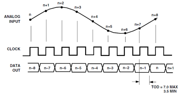
  Experiment 18 High-speed ADC9226 Acquisition Experiment 18.1 Experiment Objective Learn about parallel ADC collectors and master the use of ADC9226. 18.2 Experiment Implement Insert the ADC9226 module face up into the FPGA development board to the GPIO2 and GPIO1 ports which are next to the red-green audio module. Write programs to use this module to test 18.3 Experiment 18.3.1 ADC9226 Module Introduction ADC9226 module adopts AD9226 chip design of ADI Company. This chip is a monolithic, 12-bit, 65 MSPS analog-to-digital converter (ADC). It uses a single power supply and…

Read More
5640 power-on sequence
Experimental Manuals FII-PRA040 FPGA Board Based FPGA Tutor Risc-V

OV5640 Camera Photo Display Experiment, IIC bus, HDMI, Understand the power-on sequence of the OV5640 – FII-PRA040 Altera Risc-V Experiment 17

Experiment 17 Photo Display Experiment of OV5640 Camera 17.1 Experiment Objective Understand the power-on sequence of the OV5640 camera and the corresponding register configuration process when outputting images of different resolutions Review previous knowledge of IIC bus Review previous knowledge of HDMI 17.2 Experiment Implement Read the power-on sequence of the OV5640 datasheet, and correctly write the power-on control program according to the peripheral module schematics. Correctly write the configuration program of the OV5640 camera with a resolution of 640X480 according to the timing requirements of the SCCB interface Based…

Read More
WM8978 internal structure block diagram
Experimental Manuals FII-PRA040 FPGA Board Based FPGA Tutor Risc-V

Audio 8978 Loopback Experiment (WM8978 Audio Sub Development Board) , How I2S (Inter-IC Sound) bus work ? – – FII-PRA040 Altera Risc-V Tutorial Experiment 16

Experiment 16 8978 Audio Loopback Experiment 16.1 Experiment Objective Learn about I2S (Inter-IC Sound) bus and how it works Familiar with the working mode of WM8978. And by configuring the interface mode and selecting the relevant registers in combination with the development board, complete the data transmission and reception, and verify it 16.2 Experiment Implement Perform audio loopback test by configuring the onboard audio chip WM8978 to check if the hardware is working properly Adjust the volume output level with the keys. 16.3 Experiment 16.3.1 WM8978 Introduction WM8978 is a…

Read More
chematics of SRAM
FII-PRA040 FPGA Board Based FPGA Tutor Risc-V

How does SRAM read and write work ? Review frequency division, button debounce, and hex conversion experiment – FII-PRA040 Altera Risc-V Tutorial Experiment 15

Experiment 15 SRAM Read and Write 15.1 Experiment Objective Learn the read and write of SRAM Review frequency division, button debounce, and hex conversion experiment content 15.2 Experiment Implement Control the read and write function of SRAM by controlling the button The data written to the SRAM is read out again and displayed on the segment display In the process of reading data, it is required to have a certain time interval for each read operation. 15.3 Experiment 15.3.1 Introduction to SRAM SRAM (Static Random-Access Memory) is a type of…

Read More
Schematics of RTL8211E-VB
FII-PRA040 FPGA Board Based FPGA Tutor Risc-V

How does Ethernet work? MII, GMII, RGMII interface advantages and disadvantages, Perform a loopback test, FII-PRA040 Altera Risc-V Tutorial Experiment 14

Experiment 14 Ethernet 14.1 Experiment Objective Understand what Ethernet is and how it works Familiar with the relationship between different interface types (MII, GMII, RGMII) and their advantages and disadvantages (FII-PRA040 uses RGMII) Combine the development board to complete the transmission and reception of data and verify it 14.2 Experiment Implement Perform a loopback test to check if the hardware is working properly. Perform data receiving verification Perform data transmission verification 14.3 Experiment 14.3.1 Introduction to Experiment Principle Ethernet is a baseband LAN technology. Ethernet communication is a communication method…

Read More
HDMI interface and ADV7511 chip physical photo
Experimental Manuals FII-PRA040 FPGA Board Based FPGA Tutor Risc-V

Learn HDMI principle, Introduction to HDMI and ADV7511 Chip, HDMI Display, FII-PRA040 Altera Risc-V tutorial Experiment 13

Experiment 13 HDMI Display 13.1 Experiment Objective Review IIC protocol Review EEPROM read and write Learn HDMI principle 13.2 Experiment Implement Display different image content on the screen through the HDMI. 13.3 Experiment 13.3.1 Introduction to HDMI and ADV7511 Chip Image display processing has always been the focus of FPGA research. At present, the image display mode is also developing. The image display interface is also gradually transitioning from the old VGA interface to the new DVI or HDMI interface. HDMI (High Definition Multimedia Interface) is a digital video/audio interface…

Read More
Experimental phenomenon of LED shifting
Experimental Manuals FII-PE7030 FPGA Products Risc-V

zynq xc7z030 board – use Vivado to establish a new project, call the system resource PLL to establish the clock, Write Verilog HDL program to achieve frequency division and implement LED shifting,FII-PE7030 Experiment 1 LED Shifting Design

Experiment 1 LED Shifting Design 1.1 Experiment Objective Practice how to use the development system software Vivado to establish a new project, call the system resource PLL to establish the clock. Write Verilog HDL program to achieve frequency division and implement LED shifting Combine hardware resources for FPGA pin configuration Compile, download the program to the develop board, and verify Observe the experimental result and debug the project 1.2 Experiment Implement All LEDs light up during reset; After reset, LED lights from low to high (from right to left) in…

Read More
Experimental Manuals FII-PRX100-S FII-PRX100D FPGA Products FPGA Tutor PRX100 Risc-V

RISC-V FPGA Board Study Guide – FII-PRX100 Experimental Manuals

Version Control Version Date Descrption V1.0 10/07/2019 Initial Release V1.1 16/09/2019 Modify part of pin assignments and Ethernet description Contents: Part 1 FII-PRX100 Development System Introduction 5 1. System Design Objective 5 2. System Resource 5 3. Human-computer Interaction Interface 5 4. Software Development System 6 5. Supporting Resources 6 Part 2 FII-PRX100 Main Hardware Resources Usage and FPGA Development Experiment 6 Experiment 1 LED Shifting 6 1. Experiment Object 6 2. Create A New Project Under Vivado 6 Experiment 2 Switches and display 25 1.Experiment Objective 25 2.Start New…

Read More
Experimental Manuals FPGA Tutor Risc-V

AD,DA Experiment , write the data into PCF8591, Read the value of AD acquisition from PCF8591, – FII-PRA040 FPGA Board Experimental 12 – Altera Risc-V FPGA Tutorial :

Experiment 12 AD,DA Experiment 12.1 Experiment Objective Since in the real world, all naturally occurring signals are analog signals, and all that are read and processed in actual engineering are digital signals. There is a process of mutual conversion between natural and industrial signals (digital-to-analog conversion: DAC, analog-to-digital conversion: ADC). The purpose of this experiment is as follows: Learn about the theory of AD conversion Review the knowledge of the IIC protocol learned in the previous experiment and write the data into PCF8591 on the development board. Read the value…

Read More
Experimental Manuals FPGA Tutor Risc-V

Learning the basic principles of asynchronous IIC bus, and the IIC communication protocol, reading and writing EEPROM – Altera Risc-V IIC Protocol Transmission FPGA Tutorial – FII-PRA040 FPGA Board Experimental 11

Experiment 11 IIC Protocol Transmission 11.1 Experiment Objective Learning the basic principles of asynchronous IIC bus, and the IIC communication protocol Master the method of reading and writing EEPROM Joint debugging using logic analyzer 11.2 Experiment Implement Correctly write a number to any address in the EEPROM (this experiment writes to the register of 8’h03 address) through the FPGA (here changes the written 8-bit data value by (SW7~SW0)). After writing in successfully, read the data as well. The read data is displayed directly on the segment display. Download the program…

Read More