zynq xc7z030 board
Experimental Manuals FII-PE7030 FPGA Products

BCD decoder, Display design of hexadecimal to 7 segment display decoders, Achieve digital clock display – zynq xc7z030 board – FII-PE7030 Experiment 3 – Segment Display Digital Clock Experiment

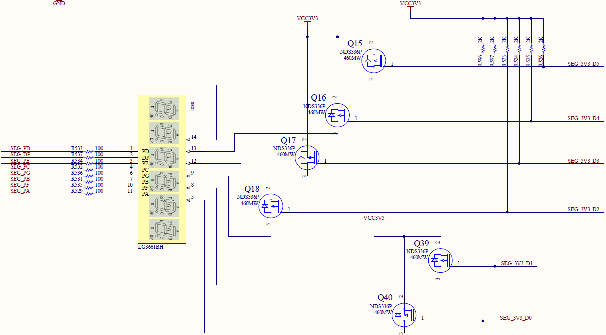
3.1 Experiment Objective Review the contents of experiment 1 and experiment 2, master the configuration of PLL, the design of frequency divider, the principle of schematics and the pin assignment of FPGA. Familiar with the design of Verilog’s tree hierarchy Study BCD decoder Display design of hexadecimal to 7 segment display decoders Achieve digital clock display 3.2 Experiment Implement The display decoder has two lower digits to display seconds, the middle two digits to display minutes, and the highest two digits to display hours. Separate the seconds, minutes, and hours…

Read More
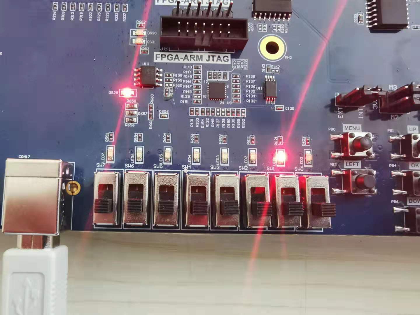
Debugging results - Analysis of Switch Signals via ILA
Experimental Manuals FII-PE7030 FPGA Products

Learn to use ILA (Integrated Logic Analyzer) in Vivado, Practice the call of system resource PLL, zynq xc7z030 board – FII-PE7030 Experiment 2

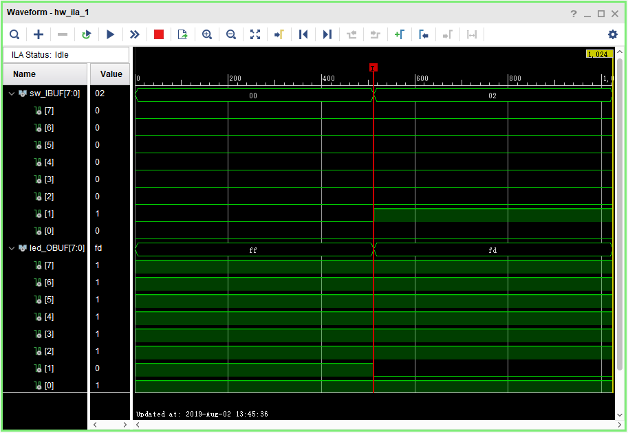
Experiment 2 Analysis of Switch Signals via ILA 2.1 Experiment Objective Continue to practice using develop board Continue to practice the call of system resource PLL Learn to use ILA (Integrated Logic Analyzer) in Vivado 2.2 Experiment Implement Capture and analyze switch signals on the development board by using ILA 2.3 Experiment 2.3.1 Introduction of Switches The on-board switch is 8 DIP switches, as shown in Figure 2.1. The switch is used to switch the circuit by turning the switch handle. Figure 2.1 Switch physical picture 2.3.2 Hardware Design The…

Read More
Experimental phenomenon of LED shifting
Experimental Manuals FII-PE7030 FPGA Products Risc-V

zynq xc7z030 board – use Vivado to establish a new project, call the system resource PLL to establish the clock, Write Verilog HDL program to achieve frequency division and implement LED shifting,FII-PE7030 Experiment 1 LED Shifting Design

Experiment 1 LED Shifting Design 1.1 Experiment Objective Practice how to use the development system software Vivado to establish a new project, call the system resource PLL to establish the clock. Write Verilog HDL program to achieve frequency division and implement LED shifting Combine hardware resources for FPGA pin configuration Compile, download the program to the develop board, and verify Observe the experimental result and debug the project 1.2 Experiment Implement All LEDs light up during reset; After reset, LED lights from low to high (from right to left) in…

Read More
FII-PE7030-Physical-Picture
FII-PE7030 FPGA Products

zynq_7030 Main Resources Usage and FPGA Development Experiemnt

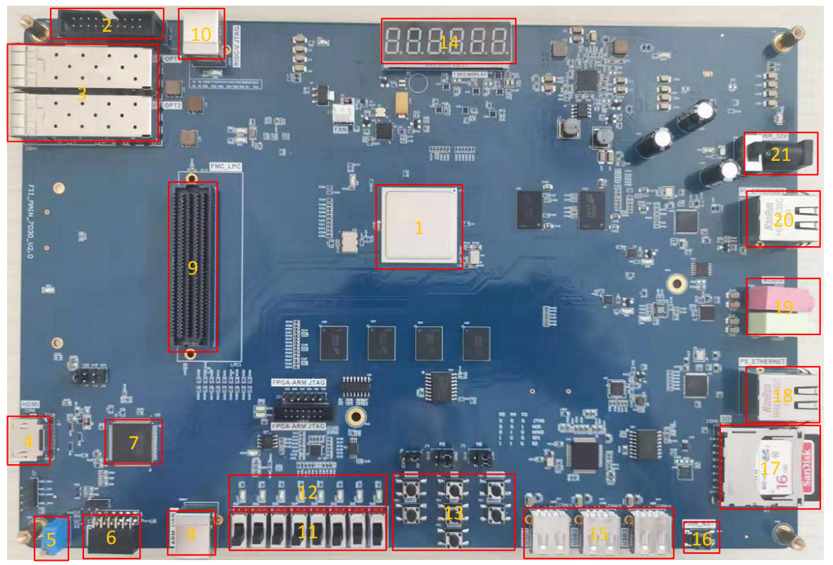
This part mainly guides the user to learn the development of FPGA program and the use of onboard hardware through the development example of FPGA. At the same time, the application system software Xilinx is introduced from the elementary to the profound. The development exercises covered in this section are as follows: Experiment 1: LED shifting design Experiment 2: ILA experiment Experiment 3: Segment display digital clock experiment Experiment 4: button debouncing experiment Experiment 5: digital clock comprehensive experiment Experiment 6: use of multiplier and ISIM simulation Experiment 7: hex…

Read More
FII-PE7030-Physical-Picture
FII-PE7030 FPGA Products

Zynq_7030 Development System FII-PE7030

System Design Objective The main purpose of this system design is to complete FPGA learning, development and experiment with Xilin-Vivado. The main device uses the XC7Z030-1FFG676C. The main learning and development projects can be completed as follows: (1)Basic FPGA design training (2)Construction and training of the SOPC (Microblaze) system (3)IC design and verification, the system provides hardware design, simulation and verification of RISC-V CPU. (4)Based on RISC-V development and application. (5)The system is specifically optimized for hardware design for RISC-V system applications. 2、System Resource Extended memory: two DDR3 (PL end)…

Read More
FII-PE7030-Physical-Picture
Experimental Manuals FII-PE7030 FPGA Board Based FPGA Products FPGA Tutor

EVB Board – Basic FPGA design training – FII-PE7030 User Experimental Manuals

Version Control Version Date Description V1.0 21/11/2019 Initial Release Contents Part One: Introduction to Zynq_7030 Development System 5 1、System Design Objective 5 2、System Resource 5 3、Human-computer Interaction Interface 5 4、Software Development System 6 5、Supporting Resources 6 6、Physical Display 6 Part Two: zynq_7030 Main Resources Usage and FPGA Development Experiemnt 8 Experiment 1 LED Shifting Design 9 1.1 Experiment Objective 9 1.2 Experiment Implement 9 1.3 Experiment 9 1.3.1 LED Introduction 9 1.3.2 Hardware Design 9 1.3.3 Program Design 10 1.4 Experiment Verification 26 Experiment 2 Analysis of Switch Signals via…

Read More
Configuration FII-PE7030 FPGA Board Based FPGA Products Hardware Reference Guide

FII-PE7030 Hardware Reference Guide

V1.1 Fraser innovation inc FII-PE7030 Hardware Reference Guide Version Control Version Date Description V1.0 08/27/2019 Initial Release V1.1 11/19/2019 Add some SD Card Part and Potentiometer Part Copyright Notice: © 2019 Fraser Innovation Inc ALL RIGHTS RESERVED Without written permission of Fraser Innovation Inc, no unit or individual may extract or modify part of or all the contents of this manual. Offenders will be held liable for their legal responsibility. Thank you for purchasing the FPGA development board. Please read the manual carefully before using the product and make sure…

Read More
Experimental Manuals FII-PRX100-S FII-PRX100D FPGA Products FPGA Tutor PRX100 Risc-V

RISC-V FPGA Board Study Guide – FII-PRX100 Experimental Manuals

Version Control Version Date Descrption V1.0 10/07/2019 Initial Release V1.1 16/09/2019 Modify part of pin assignments and Ethernet description Contents: Part 1 FII-PRX100 Development System Introduction 5 1. System Design Objective 5 2. System Resource 5 3. Human-computer Interaction Interface 5 4. Software Development System 6 5. Supporting Resources 6 Part 2 FII-PRX100 Main Hardware Resources Usage and FPGA Development Experiment 6 Experiment 1 LED Shifting 6 1. Experiment Object 6 2. Create A New Project Under Vivado 6 Experiment 2 Switches and display 25 1.Experiment Objective 25 2.Start New…

Read More
FPGA Board For Beginner with free Experimental Manuals
Experimental Manuals FPGA for Beginners FPGA Products

FPGA evb – $59 – Cyclone 10 with User Experimental Manual

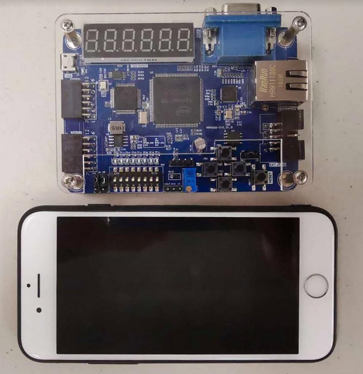
  FII-PRA006/010 User Experimental Manual Product Only $59 Product URL: PRA006 – https://fraserinnovations.com/product/altera-fpga-study-board/ PRA010 – https://fraserinnovations.com/product/fpga-study-board-verilog-and-vhdl-for-beginner-cyclone-10-fpga-development-board-with-jtag-embeded-fii-pra010/ Official Shopping Website:  https://fpgamarketing.com/FPGA-Study-Board-Verilog-for-beginner-Cyclone-10-FII-PRA006-FII-PRA006.htm We will send you official newest experimental manuals pdf file, hardware reference guide pdf file, project file zip file, Schematic Diagram pdf file when you order from above links: The advantage of FPGA evb – Cyclone 10 development board: Beginner FPGA study board, cheaper but fully functional. cellphone sized. ( < 100 USD ) power supply and download at the same time, no extra power supply and no extra data transfer…

Read More
Experimental Manuals FPGA Tutor Risc-V

AD,DA Experiment , write the data into PCF8591, Read the value of AD acquisition from PCF8591, – FII-PRA040 FPGA Board Experimental 12 – Altera Risc-V FPGA Tutorial :

Experiment 12 AD,DA Experiment 12.1 Experiment Objective Since in the real world, all naturally occurring signals are analog signals, and all that are read and processed in actual engineering are digital signals. There is a process of mutual conversion between natural and industrial signals (digital-to-analog conversion: DAC, analog-to-digital conversion: ADC). The purpose of this experiment is as follows: Learn about the theory of AD conversion Review the knowledge of the IIC protocol learned in the previous experiment and write the data into PCF8591 on the development board. Read the value…

Read More