WM8978 internal structure block diagram
Experimental Manuals FII-PRA040 FPGA Board Based FPGA Tutor Risc-V

Audio 8978 Loopback Experiment (WM8978 Audio Sub Development Board) , How I2S (Inter-IC Sound) bus work ? – – FII-PRA040 Altera Risc-V Tutorial Experiment 16

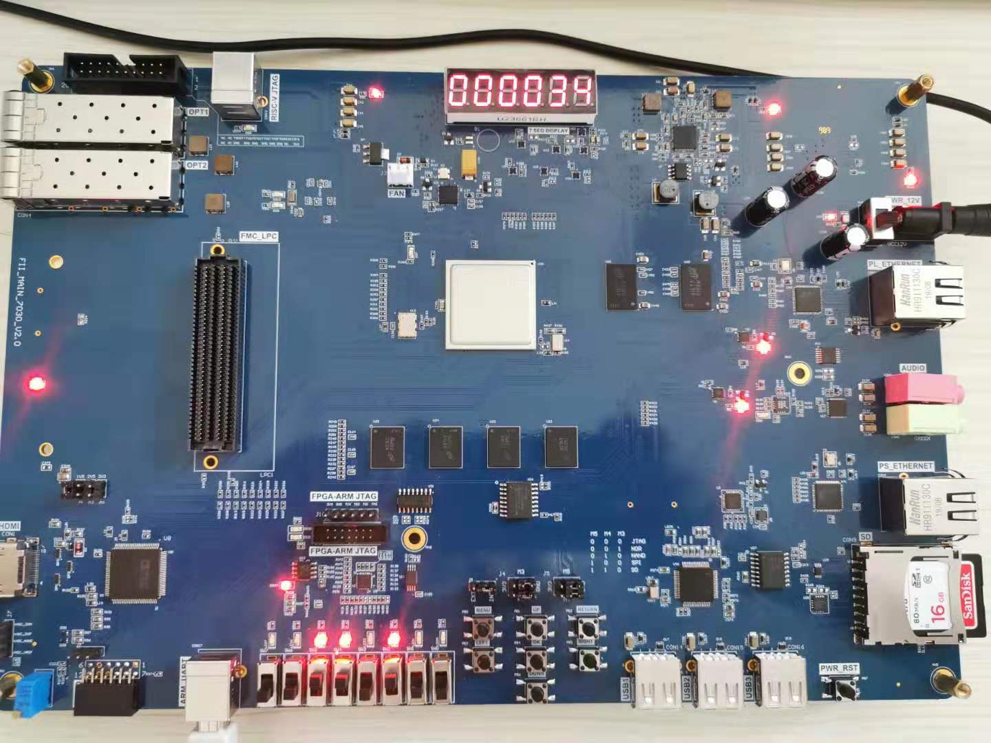
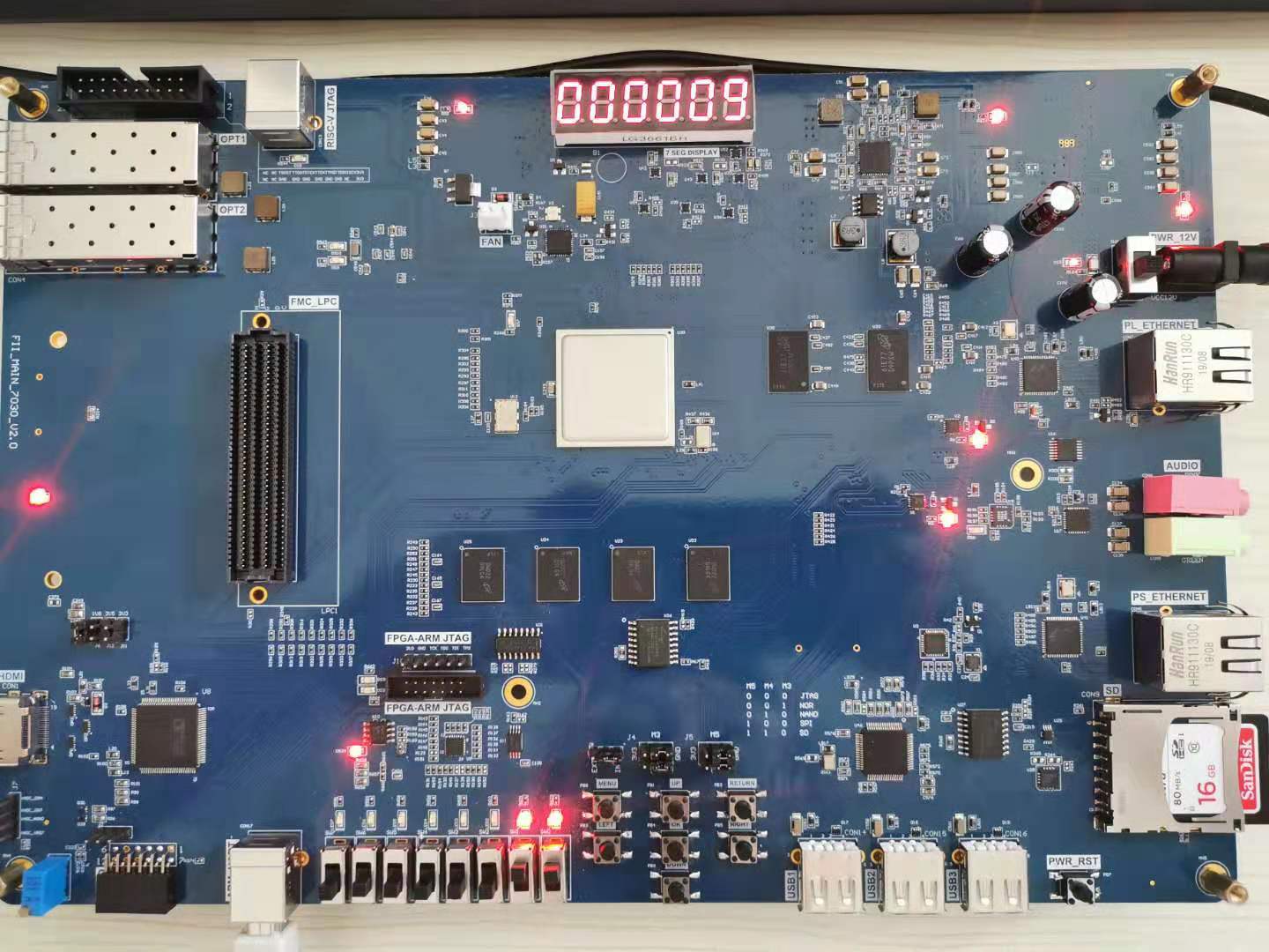
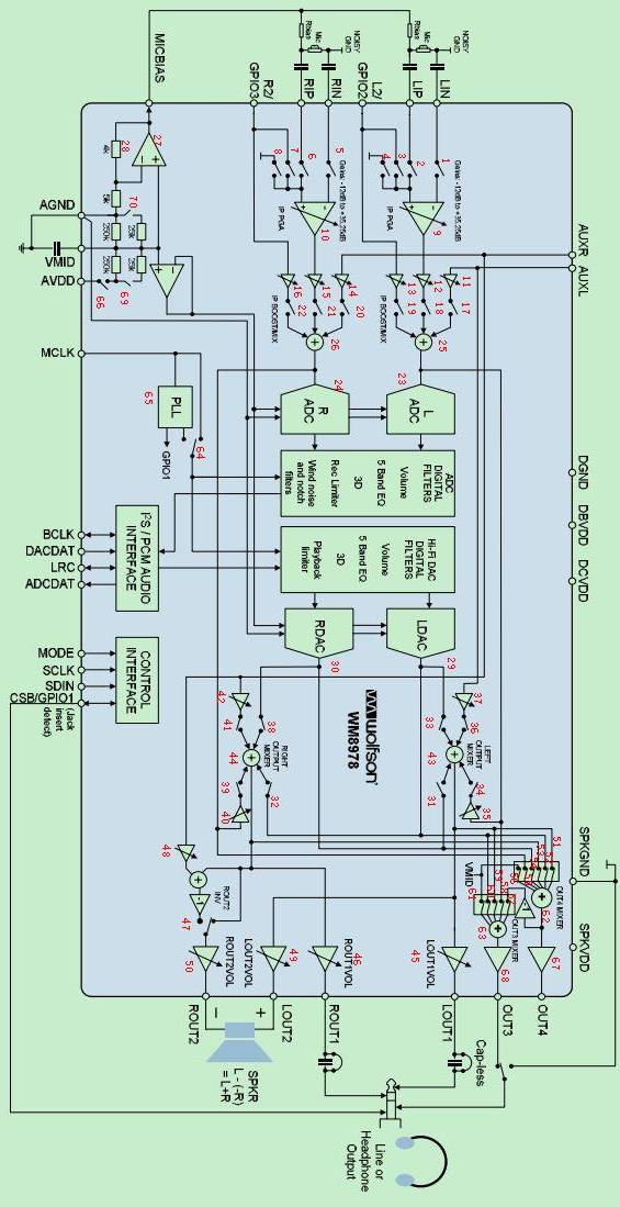
Experiment 16 8978 Audio Loopback Experiment 16.1 Experiment Objective Learn about I2S (Inter-IC Sound) bus and how it works Familiar with the working mode of WM8978. And by configuring the interface mode and selecting the relevant registers in combination with the development board, complete the data transmission and reception, and verify it 16.2 Experiment Implement Perform audio loopback test by configuring the onboard audio chip WM8978 to check if the hardware is working properly Adjust the volume output level with the keys. 16.3 Experiment 16.3.1 WM8978 Introduction WM8978 is a…

Read More
chematics of SRAM
FII-PRA040 FPGA Board Based FPGA Tutor Risc-V

How does SRAM read and write work ? Review frequency division, button debounce, and hex conversion experiment – FII-PRA040 Altera Risc-V Tutorial Experiment 15

Experiment 15 SRAM Read and Write 15.1 Experiment Objective Learn the read and write of SRAM Review frequency division, button debounce, and hex conversion experiment content 15.2 Experiment Implement Control the read and write function of SRAM by controlling the button The data written to the SRAM is read out again and displayed on the segment display In the process of reading data, it is required to have a certain time interval for each read operation. 15.3 Experiment 15.3.1 Introduction to SRAM SRAM (Static Random-Access Memory) is a type of…

Read More
Schematics of RTL8211E-VB
FII-PRA040 FPGA Board Based FPGA Tutor Risc-V

How does Ethernet work? MII, GMII, RGMII interface advantages and disadvantages, Perform a loopback test, FII-PRA040 Altera Risc-V Tutorial Experiment 14

Experiment 14 Ethernet 14.1 Experiment Objective Understand what Ethernet is and how it works Familiar with the relationship between different interface types (MII, GMII, RGMII) and their advantages and disadvantages (FII-PRA040 uses RGMII) Combine the development board to complete the transmission and reception of data and verify it 14.2 Experiment Implement Perform a loopback test to check if the hardware is working properly. Perform data receiving verification Perform data transmission verification 14.3 Experiment 14.3.1 Introduction to Experiment Principle Ethernet is a baseband LAN technology. Ethernet communication is a communication method…

Read More
HDMI interface and ADV7511 chip physical photo
Experimental Manuals FII-PRA040 FPGA Board Based FPGA Tutor Risc-V

Learn HDMI principle, Introduction to HDMI and ADV7511 Chip, HDMI Display, FII-PRA040 Altera Risc-V tutorial Experiment 13

Experiment 13 HDMI Display 13.1 Experiment Objective Review IIC protocol Review EEPROM read and write Learn HDMI principle 13.2 Experiment Implement Display different image content on the screen through the HDMI. 13.3 Experiment 13.3.1 Introduction to HDMI and ADV7511 Chip Image display processing has always been the focus of FPGA research. At present, the image display mode is also developing. The image display interface is also gradually transitioning from the old VGA interface to the new DVI or HDMI interface. HDMI (High Definition Multimedia Interface) is a digital video/audio interface…

Read More
Ethernet Experiment Information received by PC from FPGA
FII-PE7030 FPGA Board Based FPGA Products FPGA Tutor

Ethernet work mechanism, the relationship between different interface types (MII, GMII, RGMII), leanrn how to transmission and reception of data, zynq xc7z030 board – FII-PE7030 Experiment 13

Experiment 13 Ethernet 13.1 Experiment Objective Understand what Ethernet and how it works Familiar with the relationship between different interface types (MII, GMII, RGMII) and their advantages and disadvantages (here uses RGMII) Combine the development board to complete the transmission and reception of data and verify it 13.2 Experiment Implement Perform a loopback test to check if the hardware is working properly. Perform data receiving verification Perform data transmission verification 13.3 Experiment 13.3.1 Introduction to Experiment Principle Ethernet is a baseband LAN technology. Ethernet communication is a communication method that…

Read More
zynq xc7z030 board – FII-PE7030 Experiment 12 - HDMI display (color strip)
Experimental Manuals FII-PE7030 FPGA Board Based FPGA Products FPGA Tutor

IIC protocol knowledge,Learn HDMI theory – zynq xc7z030 board – FII-PE7030 Experiment 12 – HDMI Experiment

Experiment 12 HDMI Experiment 12.1 Experiment Objective Review IIC protocol knowledge Learn HDMI theory 12.2 Experiment Implement Through the HDMI interface, different image contents are displayed on the screen. 12.3 Experiment 12.3.1 Introduction to HDMI Interface and ADV7511 Chip Image display processing has always been the focus of FPGA research. At present, the image display mode is also developing. The image display interface is also gradually transitioning from the old VGA interface to the new DVI or HDMI interface. HDMI (High Definition Multimedia Interface) is a digital video/audio interface technology.…

Read More
IIC transmission experimental phenomenon
Experimental Manuals FII-PE7030 FPGA Board Based FPGA Products FPGA Tutor

asynchronous IIC bus, and the IIC communication protocol, reading and writing EEPROM – zynq xc7z030 board – FII-PE7030 Experiment 11 – IIC Protocol Transmission

Experiment 11 IIC Protocol Transmission 11.1 Experiment Objective Learning the basic principles of asynchronous IIC bus, and the IIC communication protocol Master the method of reading and writing EEPROM Joint debugging using logic analyzer 11.2 Experiment Implement Correctly write a number to any address in the EEPROM (this experiment writes to the register of 8’h03 address) through the FPGA (here changes the written 8-bit data value by (SW7~SW0)). After writing in successfully, read the data as well. The read data is displayed directly on the segment display. Download the program…

Read More
zynq xc7z030 board – FII-PE7030 Experiment 10 -Sent data received on the host computer
Experimental Manuals FII-PE7030 FPGA Board Based FPGA Products FPGA Tutor

zynq xc7z030 board – FII-PE7030 Experiment 10 – Asynchronous Serial Port Design and Experiment

10.1 Experiment Objective Because asynchronous serial ports are very common in industrial control, communication, and software debugging, they are also vital in FPGA development. Study the basic principles of asynchronous serial port communication, handshake mechanism, data frame Master asynchronous sampling techniques Review the frame structure of the data packet Learning FIFO Joint debugging with common debugging software of PC (SSCOM, teraterm, etc.) 10.2 Experiment Implement Design and transmit full-duplex asynchronous communication interface Tx, Rx Baud rate of 11520 bps, 8-bit data, 1 start bit, 1 or 2 stop bits Receive…

Read More
Use Dual-port RAM to Read and Write Frame Data
Experimental Manuals FII-PE7030 FPGA Board Based FPGA Products FPGA Tutor

zynq xc7z030 board – FII-PE7030 Experiment 9 – Use Dual-port RAM to Read and Write Frame Data

Experiment 9 Use Dual-port RAM to Read and Write Frame Data 9.1 Experiment Objective Learn to configure and use dual-port RAM Learn to use synchronous clock to control the synchronization of frame structure Learn to use asynchronous clock to control the synchronization of frame structure Use ILA to observe the structure of a synchronized clock frame Extended the use of dual-port RAM Design the use of three-stage state machine Experiment Implement Use ILA to observe the structure of a synchronized clock frame Extended the use of dual-port RAM Design the…

Read More
Experimental phenomenon of ROM usage
Experimental Manuals FII-PE7030 FPGA Board Based FPGA Products FPGA Tutor

zynq xc7z030 board – FII-PE7030 Experiment 8 – Use of ROM, Study the format of *.coe and how to edit *.coe file to configure the contents of ROM

    Experiment 8 Use of ROM 8.1 Experiment Objective Study the usage of internal memory block of FPGA Study the format of *.coe and how to edit *.coe file to configure the contents of ROM Learn to use RAM, read and write RAM 8.2 Experiment Implement Design 16 outputs ROM, address ranging 0-255 Interface 8-bit switch input as ROM’s address Segment display illustartes the contents of ROM and require conversion of hexadecimal to BCD output. 8.3 Experiment 8.3.1 Program Design The first step: the establishment of the main program…

Read More