We will list the Risc-V tutor PDF for you. You will learn step by step how to design a Risc-V CPU using our Risc-V Fpga board and our FII_RISC-V V3.01 processor. New Risc-V tutorial Manuals will be updated frequently.
What is FII_RISC-V RV32G2.0 CPU processor ?
asm_test hosts unit tests for different features of FII_RISC-V V3.01 CPU processor. This CPU is fully pipelined and include irq feature. FII_RISC-V V3.01 include mul and div instructions. Its ROM write and read depth is set to be 16384 bits. asm_test project contains test cases assembly files ,main file and header files for macros. It is build through FreedomStudio platform.asm_test will test all of the FII_RISC-V V3.01 processor supported instructions . The corresponding assembly files were stored in folder asm.
For more information, please check ASM Test Introduction
- FII RISC-V3.01 CPU Processor on FII-PRX100-S (ARTIX-7, XC7A100T) XILINX FPGA Board Evaluation Evaluation by Coremark and Dhrystone Benchmarks
- Dhrystone Porting Guide For FII RISC-V3.01 CPU Processor on FII-PRX100-S (ARTIX-7, XC7A100T) XILINX FPGA Board
- FII RISC-V3.01 CPU Processor on FII-PRX100-S (ARTIX-7, XC7A100T) XILINX FPGA Board Coremark Porting Guide
- C Programming (2) on RISCV FII-PRX100 (ARTIX-7, XC7A100T) XILINX FPGA Board with our FII-Risc-V CPU (RV32G2.0)
- C Programming (1) on RISCV FII-PRX100 (ARTIX-7, XC7A100T) XILINX FPGA Board with our FII-Risc-V CPU (RV32G2.0)
- Risc-V Bus and PipeLine – FII Risc-V Bus and Pipeline Design – Risc-V Tutorial and Exercise
- RISC-V Instruction Set Explanation
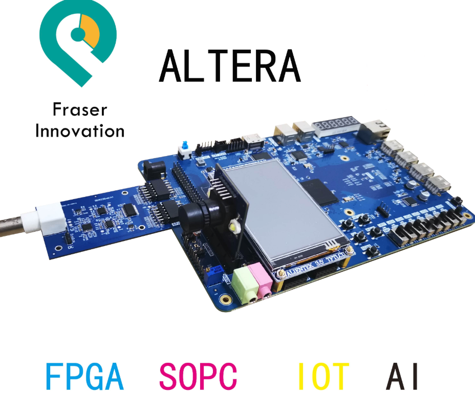
Altera Risc-V Board User Experimental Manual – PRA040
- Altera Risc-V FPGA Board Tutorial : Introduction of FII-PRA040 Development System
- Altera Risc-V FPGA Tutorial : LED shifting – FII-PRA040 FPGA Board Experimental 1
- Altera Risc-V FPGA Tutorial : SignalTap – FII-PRA040 FPGA Board Experimental 2
- Altera Risc-V FPGA Tutorial : Segment Display – FII-PRA040 FPGA Board Experimental 3
- Altera Risc-V FPGA Tutorial : Block/SCH – FII-PRA040 FPGA Board Experimental 4
- Altera Risc-V FPGA Tutorial : Button Debounce – FII-PRA040 FPGA Board Experimental 5
- Altera Risc-V FPGA Tutorial : Use of Multipliers and ModelSim – FII-PRA040 FPGA Board Experimental 6
- Altera Risc-V FPGA Tutorial : Hexadecimal Number to BCD Code Conversion and Application – FII-PRA040 FPGA Board Experimental 7
- Altera Risc-V FPGA Tutorial : Use of ROM – FII-PRA040 FPGA Board Experimental 8
- Altera Risc-V FPGA Tutorial : Use Dual-port RAM to Read and Write Frame Data – FII-PRA040 FPGA Board Experimental 9
- Altera Risc-V FPGA Tutorial :Asynchronous Serial Port Design and Experiment – FII-PRA040 FPGA Board Experimental 10
- Altera Risc-V FPGA Tutorial : IIC Protocol Transmission – FII-PRA040 FPGA Board Experimental 11
- Altera Risc-V FPGA Tutorial :AD,DA Experiment – FII-PRA040 FPGA Board Experimental 12
- Learn HDMI principle, Introduction to HDMI and ADV7511 Chip, HDMI Display, FII-PRA040 Altera Risc-V tutorial Experiment 13
- How does Ethernet work? MII, GMII, RGMII interface advantages and disadvantages, Perform a loopback test, FII-PRA040 Altera Risc-V Tutorial Experiment 14
- How does SRAM read and write work ? Review frequency division, button debounce, and hex conversion experiment – FII-PRA040 Altera Risc-V Tutorial Experiment 15
- Audio 8978 Loopback Experiment (WM8978 Audio Sub Development Board) , How I2S (Inter-IC Sound) bus work ? – – FII-PRA040 Altera Risc-V Tutorial Experiment 16
- OV5640 Camera Photo Display Experiment, IIC bus, HDMI, Understand the power-on sequence of the OV5640 – FII-PRA040 Altera Risc-V Experiment 17
- High-speed ADC9226 Acquisition Experiment (FII-BD9226) – parallel ADC collectors and master the use of ADC9226 – FII-PRA040 Altera Risc-V Experiment 18
- DAC9767 DDS Signal Source Experiment, AD9767 datasheet and use the AD9767 to design a signal source that can generate sine, square, triangle, and sawtooth waves – FII-PRA040 Altera Risc-V Experiment 19

xilinx Risc-V Board PRX100 Experimental Tutorial
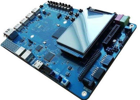
Buy RISC-V FPGA Board ( ARTIX 100T, XC7A100T ) – FII-PRX100 Development Board
- xilinx Risc-V Tutorial – FII-PRX100 – Development System Introduction
- xilinx Risc-V Tutorial – Development Board Experiment 1 – LED Shifting – FII-PRX100
- xilinx Risc-V Tutorial : Switches and Display – FII-PRX100 FPGA Board Experiment 2
- xilinx Risc-V Tutorial : Basic Digital Clock Experiment and Programming of FPGA Configuration Files- FII-PRX100 FPGA Board Experiment 3
- xilinx Risc-V Tutorial : Block/SCH Digital Clock Design- FII-PRX100 FPGA Board Experiment 4
- xilinx Risc-V Tutorial : Button Debounce Design and Experimental- FII-PRX100 FPGA Board Experiment 5
- xilinx Risc-V Tutorial : Digital Clock Comprehensive Design Experiment- FII-PRX100 FPGA Board Experiment 6
- xilinx Risc-V Tutorial : Multiplier Use and ISIM Simulation- FII-PRX100 FPGA Board Experiment 7
- xilinx Risc-V Tutorial : Hexadecimal Number to BCD Code Conversion and Application – FII-PRX100 FPGA Board Experiment 8
- xilinx Risc-V Board Tutorial : Use of ROM – FII-PRX100 Board Experiment 9
- xilinx Risc-V Tutorial : Use Dual_port RAM to Read and Write Frame Data – FII-PRX100 FPGA Board Experiment 10
- xilinx Risc-V Tutorial : Asynchronous Serial Port Design and Experiment – FII-PRX100 FPGA Board Experiment 11
- xilinx Risc-V Board Tutorial : IIC Protocol Transmission – FII-PRX100 FPGA Board Experiment 12
- xilinx Risc-V Tutorial : AD, DA Experiment – FII-PRX100 FPGA Board Experiment 13
- Xilinx Risc-V Tutorial : HDMI Graphic Display Experiment – FII-PRX100 FPGA Board Experiment 14
- How ethernet work and familiar with MII, GMII, RGMII interface types – FII-PRX100 Risc-V Board Experiment 15
- Audio 8978 Loopback Experiment – What is I2S (Inter-IC Sound) bus and how it works – AWM8978 Audio Boardudio – Xilinx Risc-V FII-PRX100 Board Experiment 16
- Reading Experiment of Serial Port Partition of Static Memory SRAM, Read and write timing of IS61WV25616BLL SRAM, and prepare for the next experimental experiment of OV5640 camera experiment – – Xilinx Risc-V FII-PRX100 Board Experiment 17
- Photo Display Experiment of OV5640 Camera , Understand the power-on sequence of the OV5640 camera and the corresponding register configuration process – Xilinx Risc-V Board FII-PRX100 Experiment 18
- High-speed ADC9226 Acquisition Experiment – Xilinx Risc-V Board FII-PRX100 Experiment 19
- DAC9767 DDS Signal Source Experiment – Xilinx Risc-V Board FII-PRX100 Experiment 20
- Xinlix Risc-V Board PRX100-S, PRX100-D Experimental Manuals (2019-12-19 Version ) with twenty experiments

What is Risc-V ?
RISC-V (pronounced “risk-five”) is a new instruction set architecture (ISA) that was originally designed to support computer architecture research and education, but now aims to become a standard open architecture for industry implementations. RISC-V was originally developed in the Computer Science Division of the EECS Department at the University of California, Berkeley.
RISC-V (pronounced “risk-five”) is an open-source hardware instruction set architecture (ISA) based on established reduced instruction set computer (RISC) principles.
RISC-V is an open ISA (instruction set architecture) enabling a new era of innovation for processor architectures. RISC-V is an open specification of an Instruction Set Architecture (ISA). It describes the way in which software talks to an underlying processor – just like the x86 ISA for Intel/AMD processors and the ARMv8 ISA for the latest and greatest ARM processors. Unlike those however, the RISC-V ISA is open so that anyone can build a processor that supports it.

Atera Risc-V FII-PRA040 Experimental Manuals ( 1- 20 ) PDF Version 2019-12-30

